Hostname: page-component-848d4c4894-x24gv Total loading time: 0 Render date: 2024-06-02T03:08:02.732Z Has data issue: false hasContentIssue false

Flexible solution-processed high-voltage organic thin film transistor

Published online by Cambridge University Press:  23 November 2017

Andy Shih*
Affiliation:
Department of Electrical Engineering and Computer Science, Microsystems Technology Laboratories, Massachusetts Institute of Technology, Cambridge, Massachusetts 02139, USA
Elizabeth Schell
Affiliation:
Department of Electrical Engineering and Computer Science, Microsystems Technology Laboratories, Massachusetts Institute of Technology, Cambridge, Massachusetts 02139, USA
Akintunde Ibitayo Akinwande
Affiliation:
Department of Electrical Engineering and Computer Science, Microsystems Technology Laboratories, Massachusetts Institute of Technology, Cambridge, Massachusetts 02139, USA
*
a)Address all correspondence to this author. e-mail: ashih@mit.edu
Get access

Abstract

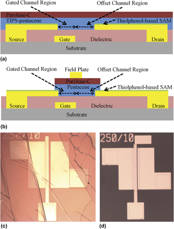
6,13-Bis(triisopropylsilylethynyl)pentacene (TIPS-pentacene) and pentacene-based high-voltage organic thin film transistors (HVOTFTs) have been fabricated on solid and flexible substrates via a low-temperature (<100 °C) solution-processed and vacuum-deposited fabrication method. A high-k dielectric Bi1.5Zn1Nb1.5O7 and an organic dielectric parylene-C have been incorporated into the transistor design. The reliability of the HVOTFTs was analyzed under flexure, where a nonsaturating IV characteristic behavior was observed. Here, the HVOTFT exhibited a mobility μ of 0.018 cm2/(V s) and a large breakdown voltage of |VDS| > 120 V and >550 V for TIPS-pentacene and pentacene devices, respectively. The large breakdown voltages are attributed to an organic semiconductor channel region which is partially gated, allowing for a large potential drop. Thiolphenol-based SAMs were used to help improve charge injection. Electrical measurements were also performed with samples designed with a top metal field plate to improve control of the charge carrier within the channel.

Type
Invited Paper
Copyright
Copyright © Materials Research Society 2017 

Access options

Get access to the full version of this content by using one of the access options below. (Log in options will check for institutional or personal access. Content may require purchase if you do not have access.)

Footnotes

Contributing Editor: Sam Zhang

References

REFERENCES

Brown, R., Jarrett, C.P., de Leeuw, D.M., and Matters, M.: Field-effect transistors made from solution-processed organic semiconductors. Synth. Met. 88, 3755 (1997).Google Scholar
Park, S.K., Jackson, T.N., Anthony, J.E., and Mourey, D.A.: High mobility solution processed 6,13-bis(triisopropyl-silylethynyl) pentacene organic thin film transistors. Appl. Phys. Lett. 91, 063514 (2007).CrossRefGoogle Scholar
Diao, Y., Shaw, L., Bao, Z., and Mannsfeld, S.C.B.: Morphology control strategies for solution-processed organic semiconductor thin films. Energy Environ. Sci. 7, 2145 (2014).CrossRefGoogle Scholar
Sirringhaus, H.: Device physics of solution-processed organic field-effect transistors. Adv. Mater. 17, 24112425 (2005).Google Scholar
Yagi, I., Hirai, N., Miyamoto, Y., Noda, M., Imaoka, A., Yoneya, N., Nomoto, K., Kashara, J., Yumoto, A., and Urabe, T.: A flexible full-color AMOLED display driven by OTFTs. J. Soc. Inf. Disp. 16(1), 1520 (2008).Google Scholar
Schwartz, G., Tee, B.C-K., Mei, J., Appleton, A.L., Kim, D.H., Wang, H., and Bao, Z.: Flexible polymer transistors with high pressure sensitivity for applications in electronic skin and health monitoring. Nat. Commun. 4, 1859 (2013).CrossRefGoogle ScholarPubMed
Tinivella, R., Camarchia, V., Pirola, M., Shen, S., and Ghione, G.: Simulation and design of OFET RFIDs through an analog/digital physics-based library. Org. Electron. 12(8), 13281335 (2011).Google Scholar
Zschieschang, U., Yamamoto, T., Takimiya, K., Kuwabara, H., Ikeda, M., Sekitani, T., Someya, T., and Klauk, H.: Organic electronics on banknotes. Adv. Mater. 23, 654658 (2011).Google Scholar
Liao, C. and Yan, F.: Organic semiconductors in organic thin-film transistor-based chemical and biological sensors. Polym. Rev. 53(3), 352406 (2013).Google Scholar
Yang, C., Yoon, J., Kim, S.H., Hong, K., Chung, D.S., Heo, K., Park, C.E., and Ree, M.: Bending-stress-driven phase transitions in pentacene thin film films for flexible organic field-effect transistors. Appl. Phys. Lett. 92, 243305 (2008).Google Scholar
Jurchescu, O.D., Popinciuc, M., van Wees, B.J., and Palstra, T.T.M.: Interface-controlled, high-mobility organic transistors. Adv. Mater. 19, 688692 (2007).CrossRefGoogle Scholar
Karim, K.S., Servati, P., and Nathan, A.: High voltage amorphous silicon TFT for use in large area applications. Microelectron. J. 35, 311315 (2004).Google Scholar
Unagami, T. and Kogure, O.: High-voltage TFT fabricated in recrystallized polycrystalline silicon. IEEE Trans. Electron Devices 35(3), 314319 (1988).CrossRefGoogle Scholar
Martin, R.A., Da Costa, V.M., Hack, M., and Shaw, J.G.: High-voltage amorphous silicon thin-film transistors. IEEE Trans. Electron Devices 40(3), 634644 (1993).Google Scholar
Ito, M., Miyazaki, C., Ishizaki, M., Kon, M., Ikeda, N., Okubo, T., Matsubara, R., Hatta, K., Ugajin, Y., and Sekine, N.: Application of amorphous oxide TFT to electrophoretic display. J. Non-Cryst. Solids 354, 27772782 (2008).Google Scholar
Kato, U., Sekitani, T., Takamiya, M., Doi, M., Asaka, K., Sakurai, T., and Someya, T.: Sheet-type braille display by integrating organic field-effect transistors and polymeric actuators. IEEE Trans. Electron Devices 54(2), 202209 (2007).Google Scholar
Zhao, W., Law, J., Waechter, D., Huang, Z., and Rowlands, J.A.: Digital radiology using active matrix readout of amorphous selenium: Detectors with high voltage protection. Med. Phys. 25(4), 539549 (1998).Google Scholar
Choi, Y., Kim, I-D., Tuller, H.L., and Akinwande, A.I.: Low-voltage organic transistors and depletion-load inverters with high-K pyrochlore BZN gate dielectric on polymer substrate. IEEE Trans. Electron Devices 52(12), 28192824 (2005).Google Scholar
Shih, A. and Akinwande, A.I.: Solution-processed high-voltage organic thin film transistor. MRS Adv. 2, 29612966 (2017).CrossRefGoogle Scholar
Chae, G.J., Jeong, S-H., Baek, J.H., Walker, B., Song, C.K., and Seo, J.H.: Improved performance in TIPS-pentacene field effect transistors using solvent additives. J. Mater. Chem. C 1, 4216 (2013).Google Scholar
Park, S.K., Anthony, J.E., and Jackson, T.N.: Solution-processed TIPS-pentacene organic thin-film-transistor circuits. IEEE Electron Device Lett. 28(10), 877 (2007).Google Scholar
Smith, M.A., Gowers, R.P., Shih, A., and Akinwande, A.I.: High-voltage organic thin-film transistors on flexible and curved surfaces. IEEE Trans. Electron Devices 62(12), 42134219 (2015).Google Scholar
Wang, L., Fine, D., Basu, D., and Dodabalapur, A.: Electric-field-dependent charge transport in organic thin-film transistors. J. Appl. Phys. 101(5), 054515 (2007).Google Scholar
Wade, J., Steiner, F., Niedzialek, D., James, D.T., Jung, Y., Yun, D-J., Bradley, D.D.C., Nelson, J., and Kim, J-S.: Charge mobility anisotropy of functionalized pentacenes in organic field effect transistors fabricated by solution processing. J. Mater. Chem. C 2, 10110 (2014).Google Scholar
Kim, H., Meihui, Z., Battaglini, N., Lang, P., and Horowitz, G.: Large enhancement of hole injection in pentacene by modification of gold with conjugated self-assembled monolayers. Org. Electron. 14, 21082113 (2013).Google Scholar
Marmon, P., Battaglini, N., Lang, P., Horowitz, G., Hwang, J., Kahn, A., Amato, C., and Calas, P.: Improving charge injection in organic thin-film transistors with tiol-based self-assembled monolayers. Org. Electron. 9, 419424 (2008).Google Scholar
Hong, J-P., Park, A-Y., Lee, S., Kang, J., Shin, N., and Yoon, D.Y.: Tuning of Ag work functions by self-assembled monolayers of aromatic thiols for an efficient hole injection for solution processed triisopropylsilylethynyl pentacene organic thin film transistors. Appl. Phys. Lett. 92, 143311 (2008).CrossRefGoogle Scholar
Shaw, J.G., Hack, M.G., and Martin, R.A.: Metastable effects in high-voltage amorphous silicon thin-film transistors. J. Appl. Phys. 69(4), 26672672 (1991).Google Scholar
Martin, R.A., Yap, P.K., Hack, M., and Tuan, H.: Device design considerations of a novel high voltage amorphous silicon thin film transistor. Proc. Int. Electron Devices Meet. 33, 440443 (1987).Google Scholar