Hostname: page-component-848d4c4894-x5gtn Total loading time: 0 Render date: 2024-06-09T08:54:29.454Z Has data issue: false hasContentIssue false

A novel terbium doping effect on physical properties of lead sulfide nanostructures: A facile synthesis and characterization

Published online by Cambridge University Press:  26 August 2020

Mohd. Shkir*
Affiliation:
Advanced Functional Materials and Optoelectronics Laboratory (AFMOL), Department of Physics, College of Science, King Khalid University, Abha61413, Saudi Arabia
Kamlesh V. Chandekar
Affiliation:
Department of Physics, Rayat Shikshan Sanstha's, Karmaveer Bhaurao Patil College, Vashi, Navi Mumbai400703, India
Thamraa Alshahrani
Affiliation:
Department of Physics, College of Science, Princess Nourah Bint Abdulrahman University, Riyadh11671, Saudi Arabia
Ashwani Kumar
Affiliation:
Department of Physics, IK Gujral Punjab Technical University, Kapurthala144603, India
Salem AlFaify
Affiliation:
Advanced Functional Materials and Optoelectronics Laboratory (AFMOL), Department of Physics, College of Science, King Khalid University, Abha61413, Saudi Arabia
*
a)Address all correspondence to this author. e-mail: shkirphysics@kku.edu.sa
Get access

Abstract

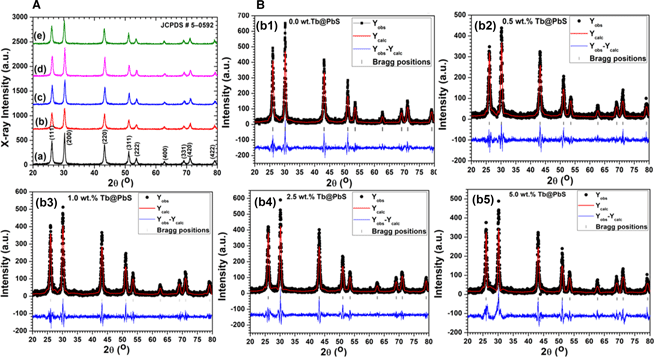
Lead sulfide (PbS) is having tremendous applications in the field of optoelectronics. Hence, a facile low temperature synthesis of PbS with different contents of terbium (Tb) has been achieved and investigated for structure–optic–dielectric–electrical properties. The structure confirmation was observed through the X-ray diffraction and Rietveld refinement process which approved a monophasic cubic structure. Rietveld refinement gives a best-fitting profile of the prepared products. The crystallite size was estimated to be in range of 15–21 nm. FT-Raman study also approved the single-phase PbS with all characteristic modes. For further confirmation of composition, homogeneity, and Tb in the final product, the EDX/SEM e-mapping was carried out. The morphological investigation was carried out through SEM which revealed that the shape and size are greatly influenced by Tb content addition in PbS. The energy gap (Eg) was estimated in the range of 1.42–1.62 eV for all Tb@PbS, and the largest Eg value was observed for 0.5 wt% Tb@PbS. The dielectric constant values are calculated in the range of 16–25 in the tested frequency region. The ac electrical conductivity was enhanced with frequency, and a charge transport mechanism is related to a correlated barrier hoping model in the prepared samples.

Type
Article
Copyright
Copyright © Materials Research Society 2020

Access options

Get access to the full version of this content by using one of the access options below. (Log in options will check for institutional or personal access. Content may require purchase if you do not have access.)

References

Liu, X. and Zhang, M.: Studies on PbS and PbSe detectors for IR system. Int. J. Infrared. Millim. 21, 1697 (2000).CrossRefGoogle Scholar
Madelung, O.: Semiconductors: Data Handbook (Springer Science & Business Media, New York, 2012).Google Scholar
Pawar, S., Shaikh, J., Devan, R., Ma, Y., Haranath, D., Bhosale, P., and Patil, P.: Facile and low cost chemosynthesis of nanostructured PbS with tunable optical properties. Appl. Surf. Sci. 258, 1869 (2011).CrossRefGoogle Scholar
Kutsenko, A., Maloletov, S., Kuchmii, S.Y., Lyakhovetskii, V., and Volkov, V.: Third-order nonlinear optical response of a new PVA composite with PbS nanocrystals theory. Exp. Chem. 38, 173 (2002).CrossRefGoogle Scholar
Souici, A., Keghouche, N., Delaire, J., Remita, H., Etcheberry, A., and Mostafavi, M.: Structural and optical properties of PbS nanoparticles synthesized by the radiolytic method. J. Phys. Chem. C 113, 8050 (2009).CrossRefGoogle Scholar
Wang, Y.: Nonlinear optical properties of nanometer-sized semiconductor clusters. Acc. Chem. Res. 24, 133 (1991).CrossRefGoogle Scholar
Kane, R., Cohen, R., and Silbey, R.: Theoretical study of the electronic structure of PbS nanoclusters. J. Phys. Chem. 100, 7928 (1996).CrossRefGoogle Scholar
Gadenne, P., Yagil, Y., and Deutscher, G.: Transmittance and reflectance in situ measurements of semicontinuous gold films during deposition. J. Appl. Phys. 66, 3019 (1989).CrossRefGoogle Scholar
Rogalski, A.: History of infrared detectors. Opto-Electron. Rev. 20, 279 (2012).CrossRefGoogle Scholar
Ni, Y., Liu, H., Wang, F., Liang, Y., Hong, J., Ma, X., and Xu, Z.: PbS crystals with clover-like structure: Preparation, characterization, optical properties and influencing factors crystal research and technology. J. Exp. Ind. Crystallogr. 39, 200 (2004).Google Scholar
Peterson, J.J. and Krauss, T.D.: Fluorescence spectroscopy of single lead sulfide quantum dots. Nano Lett. 6, 510 (2006).CrossRefGoogle ScholarPubMed
Preetha, K.C. and Remadevi, T.L.: Behavior of chemically deposited PbS thin films subjected to two different routes of post deposition annealing. Mater. Sci. Semicond. Process. 16, 605 (2013).CrossRefGoogle Scholar
Wan, Q., Huang, Q., Liu, M., Xu, D., Huang, H., Zhang, X., and Wei, Y.: Aggregation-induced emission active luminescent polymeric nanoparticles: Non-covalent fabrication methodologies and biomedical applications. Appl. Mater. Today 9, 145 (2017).CrossRefGoogle Scholar
Jiang, R., Liu, M., Chen, T., Huang, H., Huang, Q., Tian, J., Wen, Y., Cao, Q.-y., Zhang, X., and Wei, Y.: Facile construction and biological imaging of cross-linked fluorescent organic nanoparticles with aggregation-induced emission feature through a catalyst-free azide-alkyne click reaction. Dyes Pigm. 148, 52 (2018).CrossRefGoogle Scholar
Hone, F.G. and Dejene, F.B.: Six complexing agents and their effects on optical, structural, morphological and photoluminescence properties of lead sulphide thin films prepared by chemical route. J. Lumin. 201, 321 (2018).CrossRefGoogle Scholar
Xu, W., Shen, Y., Xie, A., and Huang, F.: Synthesis and characterization of PbS nanorods in W/O microemulsion system. Russ. J. Phys. Chem. A 83, 2297 (2009).CrossRefGoogle Scholar
Wang, S.F., Gu, F., and , M.K.: Sonochemical synthesis of hollow PbS nanospheres. Langmuir 22, 398 (2006).CrossRefGoogle ScholarPubMed
Antu, A.D., Jiang, Z., Premathilka, S.M., Tang, Y., Hu, J., Roy, A., and Sun, L.: Bright colloidal PbS nanoribbons. Chem. Mater. 30, 3697 (2018).CrossRefGoogle Scholar
Zhukov, N., Rokakh, A., and Shishkin, M.: Properties of lead-sulfide nanoparticles in a multicrystalline structure. Semiconductors 52, 755 (2018).CrossRefGoogle Scholar
Akbay, E. and Ölmez, T.G.: Sonochemical synthesis and loading of PbS nanoparticles into mesoporous silica. Mater. Lett. 215, 263 (2018).CrossRefGoogle Scholar
Shkir, M., Khan, A., Hamdy, M., and AlFaify, S.: A facile microwave synthesis of PbS: Sr nanoparticles and their key structural, morphological, optical, photoluminescence, dielectric and electrical studies for optoelectronics. Mater. Res. Express 6, 1250e6 (2020).CrossRefGoogle Scholar
Chen, J.-S., Zang, H., Li, M., and Cotlet, M.: Hot excitons are responsible for increasing photoluminescence blinking activity in single lead sulfide/cadmium sulfide nanocrystals. Chem. Commun. 54, 495 (2018).CrossRefGoogle ScholarPubMed
Xu, T., Hu, J., Wei, P., Qin, X., Huang, T., Chen, L., and Wu, H.: Octahedron shaped lead sulfide nanocrystals as counter electrodes for quantum dot sensitized solar cells. Funct. Mater. Lett. 11, 1850025 (2018).CrossRefGoogle Scholar
Gaiduk, A.P., Gaiduk, P.I., and Larsen, A.N.: Chemical bath deposition of PbS nanocrystals: Effect of substrate. Thin Solid Films 516, 3791 (2008).CrossRefGoogle Scholar
Saraidarov, T., Reisfeld, R., Sashchiuk, A., and Lifshitz, E.: Nanocrystallites of lead sulfide in hybrid films prepared by sol–gel process. J. Sol-Gel Sci. Technol. 34, 137 (2005).CrossRefGoogle Scholar
Koao, L., Hone, F.G., and Dejene, F.: Synthesis and characterization of PbS nanowires doped with Tb3+ ions by using chemical bath deposition method. J. Nanostruct. Chem. 10, 1 (2020).CrossRefGoogle Scholar
Shkir, M., Chandekar, K.V., Khan, A., El-Toni, A.M., and AlFaify, S.: A facile synthesis of Bi@PbS nanosheets and their key physical properties analysis for optoelectronic technology. Mater. Sci. Semicond. Process 107, 104807 (2020).CrossRefGoogle Scholar
Nakrela, A., Benramdane, N., Bouzidi, A., Kebbab, Z., Medles, M., and Mathieu, C.: Site location of Al-dopant in ZnO lattice by exploiting the structural and optical characterisation of ZnO: Al thin films. Results Phys. 6, 133 (2016).CrossRefGoogle Scholar
Pearson, G.L. and Bardeen, J.: Electrical properties of pure silicon and silicon alloys containing boron and phosphorus. Phys. Rev. 75, 865 (1949).CrossRefGoogle Scholar
Shkir, M., AlFaify, S., Yahia, I.S., Ganesh, V., and Shoukry, H.: Microwave-assisted synthesis of Gd3+ doped PbI2 hierarchical nanostructures for optoelectronic and radiation detection applications. Physics B 508, 41 (2017).CrossRefGoogle Scholar
Shkir, M., Khan, A., El-Toni, A.M., Aldalbahi, A., Yahia, I.S., and AlFaify, S.: Structural, morphological, opto-nonlinear-limiting studies on Dy:PbI2/FTO thin films derived facilely by spin coating technique for optoelectronic technology. J. Phys. Chem. Solids 130, 189 (2019).CrossRefGoogle Scholar
AlFaify, S., and Shkir, M.: A facile one pot synthesis of novel pure and Cd doped PbI2 nanostructures for electro-optic and radiation detection applications. Opt. Mater. 88, 417 (2019).CrossRefGoogle Scholar
Shakir, M., Kushwaha, S., Maurya, K., Bhagavannarayana, G., and Wahab, M.: Characterization of ZnSe nanoparticles synthesized by microwave heating process. Solid State Commun. 149, 2047 (2009).CrossRefGoogle Scholar
Shkir, M., Ashraf, I.M., Chandekar, K.V., Yahia, I.S., Khan, A., Algarni, H., and AlFaify, S.: A significant enhancement in visible-light photodetection properties of chemical spray pyrolysis fabricated CdS thin films by novel Eu doping concentrations. Sens. Actuators, A 301, 111749 (2020).CrossRefGoogle Scholar
Shkir, M., Khan, M.T., Ashraf, I.M., AlFaify, S., El-Toni, A.M., Aldalbahi, A., Ghaithan, H., and Khan, A.: Rapid microwave-assisted synthesis of Ag doped-PbS nanoparticles for optoelectronic applications. Ceram. Int. 45, 21975 (2019).CrossRefGoogle Scholar
Shkir, M., Khan, M.T., Khan, A., El-Toni, A.M., Aldalbahi, A., and AlFaify, S.: Facilely synthesized Cu:PbS nanoparticles and their structural, morphological, optical, dielectric and electrical studies for optoelectronic applications. Mater. Sci. Semicond. Process 96, 16 (2019).CrossRefGoogle Scholar
Sagadevan, S., Pal, K., Hoque, E., and Chowdhury, Z.Z.: A chemical synthesized Al-doped PbS nanoparticles hybrid composite for optical and electrical response. J. Mater. Sci.: Mater. Electron. 28, 10902 (2017).Google Scholar
Mamiyev, Z.Q. and Balayeva, N.O.: Preparation and optical studies of PbS nanoparticles. Opt. Mater. 46, 522 (2015).CrossRefGoogle Scholar
Kanimozhi, S., Vishnushankar, D., and Veeravazhuthi, V.: Structural properties of PbS nanoparticles prepared by photo chemical synthesis. Adv. Mater. Res. 678, 136 (2013).CrossRefGoogle Scholar
Liang, D., Tang, S., Liu, J., Liu, J., Lv, X., and Kang, L.: Large scale hydrothermal synthesis of PbS nanorods. Mater. Lett. 62, 2426 (2008).CrossRefGoogle Scholar
Sai, C.D., Luu, M.Q., Nguyen, P.M., Pham, N.H., Nguyen, V.T., Nguyen, X.Q., Doan, Q.K., and Tran, T.H.: Fast synthesis of PbS nanoparticles for fabrication of glucose sensor with enhanced sensitivity. J. Electron. Mater. 46, 3674 (2017).CrossRefGoogle Scholar
Priyanka, U., Akshay Gowda, K. M., Elisha, M., and Nitish, N.: Biologically synthesized PbS nanoparticles for the detection of arsenic in water. Int. Biodeterior. 119, 78 (2017).Google Scholar
Smith, G.D., Firth, S., Clark, R.J., and Cardona, M.: First-and second-order Raman spectra of galena (PbS). J. Appl. Phys. 92, 4375 (2002).CrossRefGoogle Scholar
Cao, H., Wang, G., Zhang, S., and Zhang, X.: Growth and photoluminescence properties of PbS nanocubes. Nanotechnology 17, 3280 (2006).CrossRefGoogle Scholar
Shkir, M. and AlFaify, S.: Tailoring the structural, morphological, optical and dielectric properties of lead iodide through Nd3+ doping. Sci. Rep. 7, 16091 (2017).CrossRefGoogle ScholarPubMed
Krauss, T.D. and Wise, F.W.: Raman-scattering study of exciton-phonon coupling in PbS nanocrystals. Phys. Rev. B 55, 9860 (1997).CrossRefGoogle Scholar
Nanda, K., Sahu, S., Soni, R., and Tripathy, S.: Raman spectroscopy of PbS nanocrystalline semiconductors. Phys. Rev. B 58, 15405 (1998).CrossRefGoogle Scholar
Krauss, T.D., Wise, F.W., and Tanner, D.B.: Observation of coupled vibrational modes of a semiconductor nanocrystal. Phys. Rev. Lett. 76, 1376 (1996).CrossRefGoogle ScholarPubMed
Shkir, M., AlFaify, S., Ganesh, V., and Yahia, I.S.: Facile one pot synthesis of PbS nanosheets and their characterization. Solid State Sci. 70, 81 (2017).CrossRefGoogle Scholar
Shkir, M. and AlFaify, S.: A facile low-temperature synthesis of nanosheets assembled PbS microflowers and their structural, morphological, optical, photoluminescence, dielectric and electrical studies. Mater. Res. Express. 6, 105013 (2019).CrossRefGoogle Scholar
Shkir, M., Yahia, I.S., and AlFaify, S.: A facilely one pot low temperature synthesis of novel Pt doped PbS nanopowders and their characterizations for optoelectronic applications. J. Mol. Struct. 1192, 68 (2019).CrossRefGoogle Scholar
Zhu, J., Liu, S., Palchik, O., Koltypin, Y., and Gedanken, A.: A novel sonochemical method for the preparation of nanophasic sulfides: Synthesis of HgS and PbS nanoparticles. J. Solid State Chem. 153, 342 (2000).CrossRefGoogle Scholar
Kruis, F.E., Fissan, H., and Rellinghaus, B.: Sintering and evaporation characteristics of gas-phase synthesis of size-selected PbS nanoparticles. Mater. Sci. Eng. B 69, 329 (2000).CrossRefGoogle Scholar
Berhanu, D., Govender, K., Smyth-Boyle, D., Archbold, M., Halliday, D.P., and O'Brien, P.: A novel soft hydrothermal (SHY) route to crystalline PbS and CdS nanoparticles exhibiting diverse morphologies. Chem. Commun. 45, 4709 (2006).CrossRefGoogle Scholar
Li, M., Yang, Y., Yuan, X., Liu, Y., and Zhang, L.: A new two-liquid-phase system to synthesize PbS nanoparticles with narrow size distribution. Mater. Lett. 149, 62 (2015).CrossRefGoogle Scholar
Jiang, Z., Subedi, K., Bhandari, G., He, Y., Leopold, M., Reilly, N., Lu, H.P., Zayak, A., and Sun, L.: Thickness-controlled synthesis of colloidal PbS nanosheets and their thickness-dependent energy gaps. Bull. Am. Phys. Soc. 59 (2014).Google Scholar
Aerts, M., Bielewicz, T., Klinke, C., Grozema, F.C., Houtepen, A.J., Schins, J.M., and Siebbeles, L.D.: Highly efficient carrier multiplication in PbS nanosheets. Nat. Commun. 5.1, 1-5 (2014).CrossRefGoogle ScholarPubMed
Ramin Moayed, M.M., Bielewicz, T., Noei, H., Stierle, A., and Klinke, C.: High-performance n-and p-type field-effect transistors based on hybridly surface-passivated colloidal PbS nanosheets. Adv. Funct. Mater. 28, 1706815 (2018).CrossRefGoogle Scholar
Chandekar, K.V., Shkir, M., Khan, A., and AlFaify, S.: An in-depth study on physical properties of facilely synthesized Dy@CdS NPs through microwave route for optoelectronic technology. Mater. Sci. Semicond. Process. 118, 105184 (2020).CrossRefGoogle Scholar
Shkir, M., Chandekar, K.V., Alshehri, B.M., Khan, A., AlFaify, S., and Hamdy, M.S.: A remarkable enhancement in photocatalytic activity of facilely synthesized terbium@Zinc oxide nanoparticles by flash combustion route for optoelectronic applications. Appl. Nanosci. 10, 1811 (2020).CrossRefGoogle Scholar
Nowak, M., Kauch, B., and Szperlich, P.: Determination of energy band gap of nanocrystalline SbSI using diffuse reflectance spectroscopy. Rev. Sci. 80, 046107 (2009).CrossRefGoogle ScholarPubMed
Kubelka, P. and Munk, F.: A contribution to the optics of pigments. Z. Tech. Phys. 12, 593 (1931).Google Scholar
Kortüm, G. and Vogel, J.: Die theorie der diffusen reflexion von licht an pulverförmigen stoffen1. Z. Phys. Chem. 18, 110 (1958).CrossRefGoogle Scholar
Alshehri, B.M., Shkir, M., Bawazeer, T.M., AlFaify, S., and Hamdy, M.S.: A rapid microwave synthesis of Ag2S nanoparticles and their photocatalytic performance under UV and visible light illumination for water treatment applications. Phys. E Low Dimens. Syst. Nanostruct. 121, 114060 (2020).Google Scholar
Kortüm, G., Braun, W., and Herzog, G.: Principles and techniques of diffuse-reflectance spectroscopy. Angew. Chem. Int. 2, 333 (1963).CrossRefGoogle Scholar
Urbach, F.: The long-wavelength edge of photographic sensitivity and of the electronic absorption of solids. Phys. Rev. 92, 1324 (1953).CrossRefGoogle Scholar
Shkir, M.: Effect of titan yellow dye on morphological, structural, optical, and ielectric properties of zinc(tris) thiourea sulphate single crystals. J. Mater. Res. 31, 1046 (2016).CrossRefGoogle Scholar
Khan, A., Shkir, M., Manthrammel, M.A., Ganesh, V., Yahia, I.S., Ahmed, M., El-Toni, A.M., Aldalbahi, A., Ghaithan, H., and AlFaify, S.: Effect of Gd doping on structural, optical properties, photoluminescence and electrical characteristics of CdS nanoparticles for optoelectronics. Ceram. Int. 45, 10133 (2019).CrossRefGoogle Scholar
Ge, J.P., Wang, J., Zhang, H.X., Wang, X., Peng, Q., and Li, Y.D.: Orthogonal PbS nanowire arrays and networks and their Raman scattering behavior. Chem. Eur. J. 11, 1889 (2005).CrossRefGoogle ScholarPubMed
Cardona, M. and Greenaway, D.L.: Optical properties and band structure of group IV-VI and group V materials. Phys. Rev. 133, A1685 (1964).CrossRefGoogle Scholar
Hu, L., Wang, W., Liu, H., Peng, J., Cao, H., Shao, G., Xia, Z., Ma, W., and Tang, J.: PbS colloidal quantum dots as an effective hole transporter for planar heterojunction perovskite solar cells. J. Mater. Chem. A 3, 515 (2015).CrossRefGoogle Scholar
Palomino-Merino, R., Portillo-Moreno, O., Chaltel-Lima, L., Pérez, R.G., de Icaza-Herrera, M., and Castaño, V.: Chemical bath deposition of PbS: Hg2+ nanocrystalline thin films. J. Nanomater. 2013, 45 (2013).CrossRefGoogle Scholar
Mohd, S., Ashraf, I.M., and AlFaify, S.: Surface area, optical and electrical studies on PbS nanosheets for visible light photo-detector application. Phys. Scr. 94, 025801 (2019).Google Scholar
Roduner, E.: Size matters: why nanomaterials are different. Chem. Soc. Rev. 35, 583 (2006).CrossRefGoogle ScholarPubMed
Jana, S., Thapa, R., Maity, R., and Chattopadhyay, K.: Optical and dielectric properties of PVA capped nanocrystalline PbS thin films synthesized by chemical bath deposition. Phys. E: Low-Dimens. Syst. Nanostruct. 40, 3121 (2008).CrossRefGoogle Scholar
Brza, M., Aziz, S.B., Anuar, H., and Al Hazza, M.H.F.: From green remediation to polymer hybrid fabrication with improved optical band gaps Intern. J. Mol. Sci. 20, 3910 (2019).CrossRefGoogle Scholar
Aziz, S.B.: Morphological and optical characteristics of chitosan (1− x): Cuox (4≤ x≤ 12) based polymer nano-composites: Optical dielectric loss as an alternative method for Tauc's model. Nanomaterials 7, 444 (2017).CrossRefGoogle Scholar
Tao, P., Li, Y., Rungta, A., Viswanath, A., Gao, J., Benicewicz, B.C., Siegel, R.W., and Schadler, L.S.: TiO2 nanocomposites with high refractive index and transparency. J. Mater. Chem. 21, 18623 (2011).CrossRefGoogle Scholar
Mohd, S., Khan, Z.R., Hamdy, M.S., Algarni, H., and AlFaify, S.: A facile microwave-assisted synthesis of PbMoO4 nanoparticles and their key characteristics analysis: A good contender for photocatalytic applications. Mater. Res. Express. 5, 095032 (2018).Google Scholar
Khan, A.H., Pal, S., Dalui, A., Pradhan, J., Sarma, D.D., and Acharya, S.: Solution-processed free-standing ultrathin two-dimensional PbS nanocrystals with efficient and highly stable dielectric properties. Chem. Mater. 29, 1175 (2017).CrossRefGoogle Scholar
Kaygili, O., Dorozhkin, S.V., Ates, T., Gursoy, N.C., Keser, S., Yakuphanoglu, F., and Selçuk, A.B.: Structural and dielectric properties of yttrium-substituted hydroxyapatites. Mater. Sci. Eng. C 47, 333 (2015).CrossRefGoogle ScholarPubMed
Jonscher, A.K.: Theuniversal'dielectric response. Nature 267, 673 (1977).CrossRefGoogle Scholar
Shkir, M., Ganesh, V., Yahia, I., and AlFaify, S.: Microwave-synthesis of La3+ doped PbI2 nanosheets (NSs) and their characterizations for optoelectronic applications. J. Mater. Sci.: Mater. Electron. 29, 15838 (2018).Google Scholar
Chakrabarty, N., Mukherjee, A., Sinha, S., Basu, S., and Meikap, A.: Observation of correlated barrier hopping in blue luminescent PbI2 nanoparticles. Phys. E Low Dimens. Syst. Nanostruct. 64, 134 (2014).CrossRefGoogle Scholar
Sze, S.M. and Ng, K.K.: Physics of Semiconductor Devices (John Wiley & Sons, New Jersey, United States, 2006).CrossRefGoogle Scholar
Kulshrestha, N., Chatterjee, B., and Gupta, P.N.: Characterization and electrical properties of polyvinyl alcohol based polymer electrolyte films doped with ammonium thiocyanate. Mater. Sci. Eng. B 184, 49 (2014).CrossRefGoogle Scholar
Aziz, S.B., Abdullah, R.M., Rasheed, M.A., and Ahmed, H.M.: Role of ion dissociation on DC conductivity and silver nanoparticle formation in PVA: AgNt based polymer electrolytes: Deep insights to ion transport mechanism. Polymer 9, 338 (2017).CrossRefGoogle ScholarPubMed
Aziz, S.B. and Abidin, Z.H.Z.: Ion-transport study in nanocomposite solid polymer electrolytes based on chitosan: Electrical and dielectric analysis. J. Appl. Polym. Sci. 132 (2015).CrossRefGoogle Scholar
Aziz, S.B., Hassan, A.Q., Mohammed, S.J., Karim, W.O., Kadir, M.F.Z., Tajuddin, H.A., and NMY Chan, N.: Structural and optical characteristics of PVA: C-Dot composites: Tuning the absorption of ultra violet (UV) region. Nanomaterials 9, 216 (2019).CrossRefGoogle ScholarPubMed
Aziz, S.B.: Modifying poly (vinyl alcohol)(PVA) from insulator to small-bandgap polymer: A novel approach for organic solar cells and optoelectronic devices. J. Electron. Mater. 45, 736 (2016).CrossRefGoogle Scholar
Rietveld, H.: A profile refinement method for nuclear and magnetic structures. J. Appl. Crystallogr. 2, 65 (1969).CrossRefGoogle Scholar
Lutterotti, L.: Program Maud (version 2.33).Google Scholar