Introduction
Development of nitride-based ultraviolet (UV) emitters has thus far been overshadowed by the intense effort in the InGaN-based visible light emitters.Reference Nakamura and Fasol 1 The potential usage of a compact UV light source ranges from energy-efficient indoor lighting (as a white-light source), free space satellite communication, compact chemical, environmental, and biological sensing devices, applications in medical diagnosis, treatment, and possibly optical storage. With all the rewarding promises, however, the development of UV emitters faces many challenging issues. Preliminary work in the AlGaN/GaN quantum well (QW) UV emittersReference Han, Crawford, Shul, Figiel, Banas, Zhang, Song, Zhou and Nurmikko 2 suggested that the use of a binary GaN active region results in a low optical output power. Furthermore, mismatch-induced tensile stress was observed during growth of AlGaN heterostructures on thick GaN templates for UV devices,Reference Han, Crawford, Shul, Hearne, Chason, Figiel and Banas 3 leading to relaxation through crack generation. Quaternary AlGaInN compound semiconductors are expected to enclose a finite (non-zero) area on the plot of energy gap versus lattice constant. In principle the employment of quaternary compounds should render flexibility in tailoring bandgap profile while maintaining lattice matching and structural integrity. In this paper we will summarize our investigation on the issues of optical efficiency and strain control using quaternary AlGaInN compound.
Experimental Details
The MOVPE growth is carried out in a vertical rotating-disc reactor. All of the quaternary epilayers and multiple quantum well (MQW) structures were grown on 1-µm GaN epilayers at 1050°C using a standard two-step nucleation procedure (on sapphire) with low-temperature GaN grown at 550 °C.Reference Han, Ng, Biefeld, Crawford and Follstaedt 4 The growth temperature of the quaternary AlGaInN was varied between 750 and 820 °C. The reactor pressure was held constant at 200 Torr. The NH3 and N2 flows were set at 6 l/min each. An additional flow of H2 (∼400 cm3/min) was employed as a carrier gas. Trimethylgallium, triethylaluminum, and trimethylindium were employed as metalorganic precursors.
Given the scarcity of reliable information concerning the quaternary, it is imperative to accurately determine the concentrations of the constituent elements. Concentrations of In and Al in the films were measured using Rutherford backscattering spectrometry (RBS)Reference Chu, Mayer and Nicolet 5 with a 2.5 MeV 4He+ ion beam. Ion-channeling effects in the RBS spectra were randomized by tilting the sample 10° from normal to the analysis beam and continuously rotating the sample about its normal during the analysis. Al and In concentrations were then extracted from the spectra using the SIMNRA (ver. 4.4) simulation program.Reference Mayer 6 Figure 1 shows a representative RBS spectrum from AlGaInN. The solid line is the fitted simulation, while the dashed line is a simulation for the same In concentration with no Al. The inset shows a diagram of the measured film on GaN, along with the fitted concentration values for In and Al. The large backscattering yield from In, coupled with the accurately known nuclear cross section, results in a relatively high accuracy for the determination of the In concentration. We estimate an uncertainty of ±0.002 at an In concentration of 0.01, and ±0.005 for a concentration of 0.10. Because the backscattering yield from Al is much smaller, the Al concentration was determined less directly by measuring a reduction, or dip, in the yield from Ga, due to the presence of the Al and In in the layer. An uncertainty of ±0.01 at an Al concentration of 0.10, and ±0.02 for a concentration of 0.20 was estimated for the cited data.

Figure 1. An RBS spectrum from an AlGaInN sample. The solid line is a simulated fit.
A high-resolution triple-axis x-ray diffractometer (Philips X’Pert System) was employed to assess the structural quality and determine both in-plane ( a ) and out-of-plane ( c ) lattice parameters using symmetric (0002) and asymmetric (202-4) (using grazing-incidence) diffractions. Photoluminescence (PL) was measured using a HeCd laser (325 nm) as the excitation source in conjunction with a 0.3 meter spectrometer and a UV enhanced CCD detector. Typical excitation level is around 30 W/cm2. Real time wafer curvature measurements were performed with a multi-beam optical stress sensor (MOSS)Reference Taylor, Barlett, Chason and Floro 7 modified for use on our reactor. To determine the wafer curvature, the divergence of an array of initially parallel laser beams is measured on a CCD camera after reflection of the array from the film/substrate surface. Changes in wafer curvature induce a proportional change in the beam spacing on the camera. This technique provides a direct measurement of the stress-thickness product during MOVPE of GaN.Reference Hearne, Chason, Han, Floro, Hunter and Figiel 8
In attempting to extract band gap energy from a PL measurement for the AlGaInN quaternary system, one is reminded that the determination of band gap energy for GaInN has been a subject of much debate.Reference Takeuchi, Takeuchi, Sota, Sakai, Amano and Akasaki 9 Indium-related compositional fluctuation is expected to contribute to a Stokes-like shift with a magnitude of less than 100 meV.Reference Chichibu, Azuhata, Sota and Nakamura 10 Field-induced separation of electrons and holes (due to piezo- and spontaneous polarization) causes a red shift (up to 300 meV) of PL emission energy in quantum well structuresReference Chichibu, Deguchi, Sota, Wada and Nakamura 11 but should not be of significance in epilayers thicker than 50 nm. Finally, the existence of a compressive or tensile biaxial strain, due to a combination of lattice mismatchReference Ambacher 12 and thermal mismatch,Reference Hearne, Chason, Han, Floro, Hunter and Figiel 8 introduces a blue or red shift, respectively, to the band gap energy as determined by the deformation potentials.Reference Kisielowski, Kruger, Ruvimov, Suski, Ager, Jones, Liliental-Weber, Rubin, Weber, Bremser and Davis 13 Given that the In fraction is limited to 10% and the pseudomorphic strain in the quaternary does not exceed 1% in compression, we estimate (using published deformation potentialsReference Chichibu, Shikanai, Azuhata, Sota, Kuramata, Horino and Nakamura 14 ) that the difference between PL emission energy and band gap to be less than 100 meV in the epilayers reported here.
Results and Discussion
GaN and GaN:In Active region Study
In our earlier work we have shown an AlGaN/GaN QW LED emitting at a wavelength of 354 nm.2 The power output of the prototype UV emitter was around 13 µW at a current level of 20 mA, which is about 2 orders of magnitude lower than the commercial high-brightness blue LEDs. A series of test samples, consisted of 0.5 µm of GaN test layers grown on a standard GaN epilayer (of 1 µm thick), were grown to optimize the optical quality of the active region. Photoluminescence (PL) at room temperature (RT) was employed to measure the optical quality. Among the growth parameters investigated, reactor pressure was found to have a distinct effect on the PL emission intensity. As the growth pressure was increased from 80 Torr (the pressure employed in the previous LEDs and chosen to mitigate the gas-phase reaction during growth of AlGaN) to 250 Torr, integrated PL intensity increased by more than 10 times and peaked at around 200 Torr. The mechanism responsible for the observed enhancement of GaN emission is not known. One might speculate that a reduction of carbon incorporation, due to an increase of the partial pressures of both NH3 and H2, reduces the non-radiative recombination paths.Reference Bedair 15
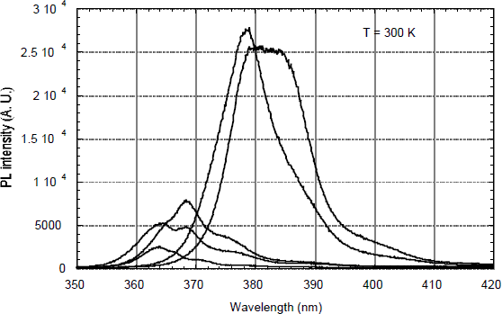
Recently it has been reported by several groupsReference Mukai, Morita and Nakamura 16 , Reference Narukawa, Saijou, Kawakami, Fujita, Mukai and Nakamura 17 , Reference Shen and Aoyagi 18 that the addition of a small amount of indium could lead to an enhancement in PL emission efficiency. Mukai et al.Reference Mukai, Morita and Nakamura 16 demonstrated an GaN:In UV LED with an indium content of around 2% and optical power output as high as 5 mW. A series of GaN:In samples (0.2 µm thick on 1 µm GaN epilayers) were grown in which the indium fraction was increased from 0 to approximately 4% as determined by x-ray and RBS. Figure 1 shows the PL spectrum of the GaN:In layers with the spectrum from an “optimized” GaN layer as a reference (the bottom trace peaking at 364 nm). At the expense of a shift of emission peak toward longer wavelengths (∼380 nm), we attained an increase of more than one order of magnitude in integrated light intensity. Two explanations have been offered to explain the observed enhancement in light emission: carrier localization due to indium incorporationReference Mukai, Morita and Nakamura 16 or the suppression of non-radiative recombination defects in the presence of indium.Reference Narukawa, Saijou, Kawakami, Fujita, Mukai and Nakamura 17 Details of the optical investigation will be reported in a separate article in this proceeding.Reference Crawford 19

Figure 2. PL of GaInN epilayers with various amount of Indium. The integrated intensity increases by more than 10 times from GaN to 4% GaInN.
Quaternary AlGaInN
Only limited information has been published concerning the AlGaInN quaternary system. MatsuokaReference Matsuoka 20 predicted the presence of an unstable mixing region (spinodal phase separation) in wurtzite AlGaInN as the indium content increases. The challenges associated with the growth of AlGaInN, primarily the selection of conditions necessary to enable surface diffusion of Al and Ga species while at the same time preventing the surface re-evaporation of In, are partially manifested by the scarcity of experimental data. McIntosh et al.Reference McIntosh, Boutros, Roberts, Bedair, Piner and El- Masry 21 and Yamaguchi et al. Reference Yamaguchi, Kariya, Nitta, Kato, Takeuchi, Wetzel, Amano and Akasaki 22 reported the physical incorporation of Al and In into GaN by MOVPE. Aiming at proof-of-concept demonstrations of material synthesis, little information was provided in either work concerning the bandgap versus alloy compositions. The functional feasibility of AlGaInN as a confinement barrier also remained ambiguous in these studies since PL emission (energies) from samples investigated did not exceed the emission (energy) of GaN (∼363 nm/ 3.42 eV)). The concern was reiterated by Peng et al.Reference Peng, Piprek, Qiu, Olowolafe, Unruh, Swann and Schubert 23 in stating, based on optical absorption measurements of sputtered polycrystalline films, that AlInN and AlGaInN do not seem to provide good confinement (to GaInN) due to a very strong bowing effect. We have shown from in-situ stress measurement that the use of high Al-fraction (or thick) AlGaN barriers on GaN templates, required for electrical and optical confinement in UV devices, leads to a buildup of tensile stress and subsequently the occurrence of cracking. Reference Han, Crawford, Shul, Hearne, Chason, Figiel and Banas 3 As discussed in the above section, introducing indium into GaN greatly enhances the optical efficiency but at the cost of an increase in emission wavelength. Investigation of quaternary AlGaInN was initiated by the two constraints encountered in the use of ternaries AlGaN and GaInN as barriers and wells, respectively. It is expected that AlGaInN would render flexibility in controlling the mismatch strain and bandgap profile.
Figure 3 shows (0002) 2θ−ω x-ray diffraction (XRD) scans (with an analyzer-crystal detector) for several AlGaInN (a, c-f) and GaInN (b) epilayer samples. Thickness of the samples varies from 0.14 to 0.20 µm, as indicated by the change of the period of the diffraction fringes. (Thin film thickness derived independently from x-ray fringes and from RBS simulations differed by less than 5% in most cases.) By adjusting the relative Al and In compositions, one observes a change of the out-of-plane lattice parameter from being larger (top trace) to smaller (bottom trace) than that of GaN. Pseudomorphic growth is verified by measuring the in-plane lattice parameter ( a ) of the epilayers. Unlike the case in zincblende semiconductor heterostructure, the appearance of an overlap between the (0002) diffraction peak from the quaternary and the peak from GaN (a condition between scans (d) and (e)) does not necessarily imply a lattice-matched strain-free epitaxy as the in-plane and out-of-plane lattice parameters of AlN, GaN, and InN do not vary in a linear manner. Using the published lattice parameters,Reference Ambacher 12 exact match of the a lattice constant of AlInN to GaN should occur at an Al fraction of 18% while it takes approximately 28% Al in AlInN to match the out-of-plane ( c ) lattice parameter of GaN. A quaternary compound with a c lattice parameter matched to GaN is speculated to be under biaxial compression during growth.

Figure 3. (0002) 2θ-ωx-ray diffraction of AlGaInN (solid traces) and GaInN (dashed line) epilayers showing a range of lattice parameters bracketing the GaN lattice parameter. The (0002) GaN diffraction peaks move progressively toward higher-angle side as the lattice parameters of the upper alloy layers reduce.
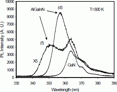
Optical properties of the AlGaInN samples (d and f in Figure 3) were investigated with RT PL (Figure 4). The PL from a “standard” GaN epilayer was included for comparison. It is clear from Figure 4 that the AlGaInN epilayer emits with energy higher than that of GaN. The Al0.14Ga0.82In0.04N epilayer (sample (d) in Figures 3 and 4) gives the indication that one can synthesize a wider bandgap (than GaN) quaternary AlGaInN compound yet with an in-plane lattice constant larger than that of GaN. It is worth noting that the integrated PL intensity from this quaternary is about three times brighter than that from GaN. There has been much empirical observation and speculation that the presence of indium in GaInN ternary layers seems to preserve excited carriers from recombining at non-radiative centers.Reference Chichibu, Marchand, Minsky, Keller, Fini, Ibbetson, Fleischer, Speck, Bowers, Hu, Mishra, DenBaars, Deguchi, Sota and Nakamura 24 Mukai et al. Reference Mukai, Morita and Nakamura 16 reported, in the development of ultra-violet LEDs, a rapid reduction of optical efficiency as the In content in the GaInN active region decreased below a certain value. The implication is that the carrier-localization effect,Reference Chichibu, Marchand, Minsky, Keller, Fini, Ibbetson, Fleischer, Speck, Bowers, Hu, Mishra, DenBaars, Deguchi, Sota and Nakamura 24 possibly due to the presence of a compositional fluctuation of indium, could make AlGaInN an alternative (to GaN or AlGaN) as a short-wavelength (λ<360nm) light-emitting medium

Figure 4. Room-temperature photoluminescence from a GaN (solid line) epilayer and two AlGaInN epilayers (samples d and f).
For the design and implementation of quaternary heterostructure devices, it is helpful to superimpose contours of constant lattice parameter and “bandgap” (or more precisely, PL peak ) energy as functions of the alloy compositions. A series of AlGaInN, GaInN, and AlGaN epilayers have been grown and the characterizations are summarized in Figure 5. AlyGa1−x−yInxN is described in this work by a right-angle triangle with AlGaN and GaInN forming the two sides around the right-angle vortex. (The hypotenuse corresponds to the ternary AlInN, not shown in Figure 5.) The location of any AlyGa1−x−yInxN quaternary is uniquely specified by the In (x) and Al (y). The triangles, diamonds, and circles represent the data points for AlGaN, GaInN, and AlGaInN, respectively. The compositions of the ternaries were determined primarily by x-ray diffraction and independently confirmed by RBS, the quaternary compositions were determined by RBS. The solid line with a slope of around 4.4 defines the quaternary alloys that are lattice matched to GaN; one can construct an array of parallel lines for lattice-matched growth with different in-plane lattice parameters. (Vegard’s law predicts that the in-plane lattice parameter will remain unchanged when the increments of Al (ΔAl) and In (ΔIn) maintain a ratio of 4.44.) Quaternary alloys located to the lower right half of the straight line are expected to be under compression on a GaN template. The distance between a given data point on this plot and the solid line gives a qualitative measure of mismatch-induced strain.

Figure 5. Contour plot of constant (in-plane) lattice parameter and emission energy versus Al and In compositions for AlGaInN epilayers.
PL investigation of the near band-edge emission is summarized by the dashed curves (denoting contours of constant PL peak energy) in Figure 5. The dashed contours are derived based on two assumptions: i) all the data points should be fitted by contours with nearly identical forms, and ii) the contours should be consistent with the available (theoreticalReference Wright and Nelson 25 and experimentalReference Kim, Saxler, Kung, Razeghi and Lim 26 ) bowing information of ternary AlInN. Along each dashed line, the emission wavelength remains constant while the in-plane lattice parameter (and therefore strain) can be adjusted by varying the Al and In fractions. Since the In-related Stokes-shift tends to increase with an increasing In composition, the slopes of the contours for the actual bandgap energy might be less steep.
AlGaInN/GaInN Multiple Quantum Wells
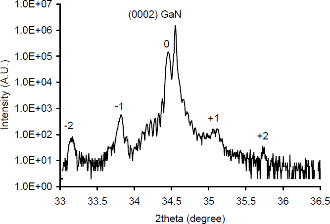
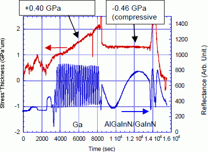
To demonstrate the possibility of heterostructures incorporating quaternary AlGaInN, we have grown multiple quantum well (MQW) structures consisting of 10 periods of AlGaInN barriers (Al∼14%, In∼4%, ∼100Å) and GaInN wells (In∼4%, ∼45Å). Figure 6 shows the (0002) 2θ−ω XRD from the MQW structure. The presence of satellite peaks and other interference fringes is indicative of structural order and coherency (along the growth direction). Cross-sectional TEM images (Figure 7) indicated that the AlGaInN/GaInN interfaces are smooth and coherent on the atomic scale. One also notices from Figure 6 that the AlGaInN/GaInN MQW has a zero-order peak that corresponds to the lattice constant of a 2.0% GaInN alloy. In-situ stress/strain monitoring was conducted during the growth of a similar MQW structure and is shown in Figure 8. While the GaN layer is under tensionReference Hearne, Chason, Han, Floro, Hunter and Figiel 8 during growth (0.40 GPa), the AlGaInN/GaInN MQW region is under compression during growth (∼0.47±0.07 GPa). Assuming a compressive thermal mismatch stress of 0.2 GPa from 1050°C to 800°C, one can estimate an average compressive mismatch strain of 0.15%, corresponding to the lattice constant of a 1.4% GaInN epilayer.

Figure 6. (0002) 2θ-ω x-ray diffraction of an AlGaInN (100Å)/GaInN (45Å) multiple (10) quantum wells.

Figure 7. Cross-sectional TEM image of an AlGaInN (100Å)/GaInN (45Å) multiple (10) quantum wells.

Figure 8. In-situ stress measurement of during growth of an MQW LED.
Optical quality of the AlGaInN/GaN MQWs was investigated using temperature-dependent PL. It is generally assumed that the non-radiative recombination mechanisms are thermally activated and the decay of integrated PL intensity from low temperature to room temperature renders a quantative measurement of the nonradiative processes.Reference Leroux, Grandjean, Beaumont, Nataf, Semon, Massies and Gibart 27 , Reference Narukawa, Kawakami, Fujita and Fujita 28 Figure 9 shows the temperature-dependent PL with a plot of the integrated intensity in the inset. A reduction of 4.5 times of the integrated PL intensity from 4K to RT is comparable to the best reported for GaInN MQWs emitting at around 450 nm.Reference Chichibu 29 This also implies that an upper limit to the internal quantum efficiency of 20% is obtained at RT.

Figure 9. Temperature-dependent PL (at 10, 75, 150, and 295 K with decreasing intensity) suggesting an internal quantum efficiency of around 20% from the AlGaInN/GaInN MQWs.
Conclusions
In conclusion, we reported the MOVPE growth and characterization of quaternary AlGaInN. Contours of constant PL peak energy and lattice parameter of AlGaInN were projected onto a two-dimensional plot. We confirmed that the employment of this novel quaternary compound could facilitate the tailoring of energy gap and lattice mismatch for design flexibility. In spite of the previous speculation that strong bowing could hinder the usage as a short-wavelength light emitter, we observed PL emission as short as 351 nm from a layer with about 20% Al and 5% In. The possibility of replacing AlGaN as an alternative barrier material was demonstrated through an AlGaInN/GaInN MQW structure.
Acknowledgements
The authors acknowledge stimulating interactions with J. Y. Tsao, A. F. Wright, S. R. Lee, and H. Amano (Meijo University). Sandia is a multiprogram laboratory, operated by Sandia Corporation, a Lockheed Martin company, for the United States Department of Energy, under contract DE-AC04-94AL8500.