Introduction
The ZEISS ORION Helium Ion Microscope (HIM) was commercially introduced in 2006 [Reference Ward1–Reference Hlawacek and Gölzhäuser3] and has rapidly become a widely used tool for high-resolution imaging and nano-fabrication. The HIM offers sub-nanometer resolution, large depth of field, and special image contrast mechanisms. To add a materials analysis capability, a helium backscatter spectrometer was added in 2009 [Reference Sijbrandij4], though the applications for that technique were somewhat limited. By 2012 the capability of using neon was added [Reference Rahman5,Reference Notte6] and commercialized as the ZEISS ORION NanoFab. The neon ion beam, with its increased sputter rate compared to helium, expanded the application-space for nanoscale sample modification processes [Reference Stanford7] and enabled secondary ion imaging.
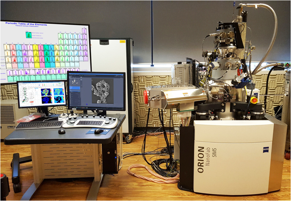
Analytical capability was added to the NanoFab in the form of a custom-designed secondary ion mass spectrometer (SIMS) [Reference Wirtz8–Reference Dowsett and Wirtz10] developed through collaboration with the Luxembourg Institute of Science and Technology (LIST) and Lion Nano-Systems, starting in 2012. The well-developed SIMS technique is based on the identification of secondary ions characteristic of surface elements, when these elements are sputtered by bombardment with a primary ion beam. This is a powerful method for analyzing surfaces because of its excellent sensitivity for elements (detection limits down to the ppb), high dynamic range, and its ability to differentiate isotopes of most elements. The SIMS designed for the NanoFab was optimized to take advantage of the small primary beam probe-size, resulting in the highest available spatial resolution SIMS capability. A 2017 prototype of the ZEISS NanoFab SIMS is shown in Figure 1. The remainder of this article focuses mainly on instrumental aspects of the combined NanoFab SIMS instrument. While a few results are included here, another article focused primarily on applications of the new instrument will appear in an upcoming issue.
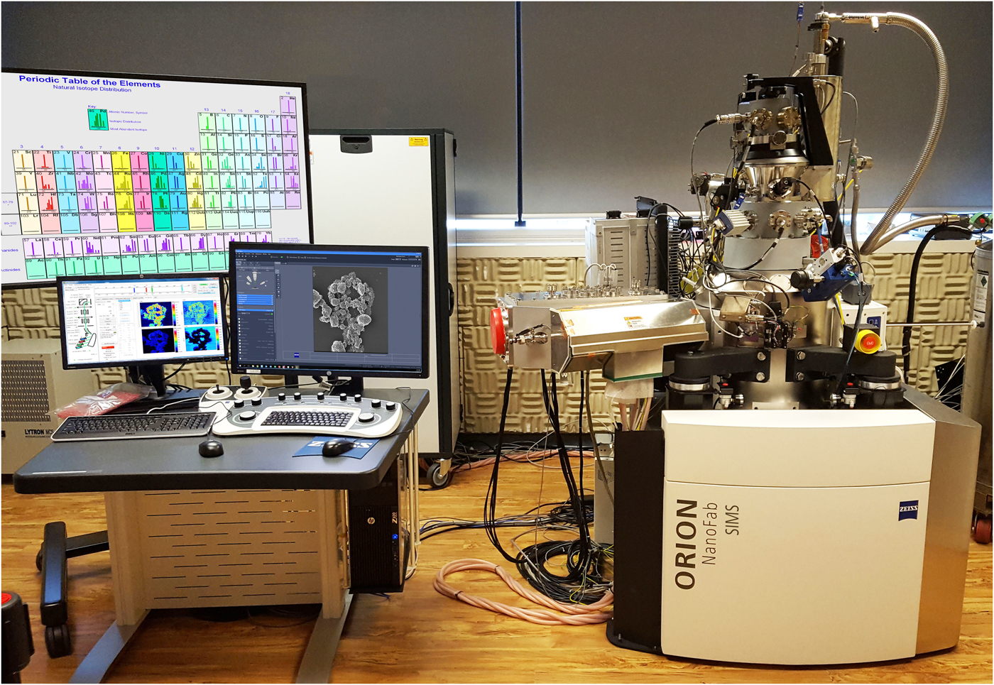
Figure 1: Photo of ORION NanoFab SIMS prototype. Operator console is on the left, and the primary beam column is on the right. The SIMS accessory is mounted on the left side of the column and occupies the center of the image.
Instrumentation
Primary ion beam platform and microscope
The defining characteristic of the NanoFab is its gas field-ionization source (GFIS), with the following optical properties: high brightness > 5 × 10⁹ A cm−2 sr−1, small virtual source size < 0.1 nm, and low energy spread < 1 eV. The ion beam can be focused to a probe-size of < 0.5 nm for He+ and < 1.9 nm for Ne+, when matched with a well-designed electrostatic ion optical column. The beam current is adjustable from 100 fA to 100 pA. Other crucial parts of the optical system include high-stability high-voltage power supplies and a liquid-nitrogen-based cryogenic system for cooling the source. The acceleration voltage can be operated in the range of 10–30 kV. The vacuum system achieves ~10−10 Torr base pressure in the source region and ~10−7 Torr in the work-chamber. To avoid issues with vibration, the system is solidly constructed with a 2-stage anti-vibration system at its base.
The work-chamber is equipped with a 5-axis motorized stage (X,Y,Z, Rotation, Tilt). Samples are transported onto the stage via a load-lock. The work-chamber also houses an Everhart-Thornley (ET) detector to collect the SE signal when imaging with the He+ beam and an electron flood-gun for charge neutralization on insulating samples. The chamber has numerous extra ports to accommodate additional equipment and accessories. The system is computer-controlled for all normal operating functions, such as instrument setup and control, scan control, and image acquisition.
Spectrometer integration
The spectrometer is designed to fit onto the NanoFab without major platform modifications. The spectrometer comes with its own electronics rack—housing power supplies, motion controllers, and data-acquisition hardware—as well as a computer to facilitate instrument control and communications with the NanoFab. Similar to the manner in which an energy-dispersive X-ray spectroscopy (EDS) system is typically added to a scanning electron microscope (SEM), the integration between the SIMS system and NanoFab platform is straightforward. The SIMS spectrometer is run with its own dedicated software. It uses the NanoFab's remote API (application programming interface) via an Ethernet connection to access features, functions, and data on the NanoFab. When the spectrometer is activated, the NanoFab's scanning system is placed in external mode, and the SIMS scanning system takes over control of the primary ion beam. The API is also used for the communication of NanoFab settings so that these can be saved within the SIMS data files. Where safety is concerned, hardware interlocks are used.
The SIMS software performs the main instrument control and data-acquisition functions. The SIMS instrument control functions include setting and reading instrument voltages, magnetic field, specimen positions, and the reading and display of ion detection rates (for instrument tuning). Data-acquisition and visualization functions for the SIMS include setting the analysis parameters, data-analysis options, and live display during acquisition for the three main data types: mass spectra, depth profiles, and elemental maps.
Mass spectrometer
The front-end of the spectrometer, consisting of the secondary ion extraction and transport optics, is retractable (Figure 2). When retracted, the system behaves and performs identically to a standard NanoFab system not equipped with SIMS. When inserted, the ion extractor is situated between the primary ion beam column and the sample. A circular 500 μm diameter opening in the extractor allows the primary beam to pass through. The sample is biased positively or negatively to provide the first acceleration stage for the secondary ion beam, which is then deflected sideways toward the spectrometer. The secondary beam then undergoes a second stage of acceleration and is transported to the spectrometer entrance by secondary ion transfer optics (Figure 2).

Figure 2: Simplified schematic illustrating the operation of the mass spectrometer. See text for details.
The spectrometer is in the familiar double-focusing magnetic sector configuration and uses a water-cooled 0.75 mT (max) electromagnet. The system employs five channel electron multipliers for ion detection. One detector is placed before the magnetic sector, enabling measurement of the total non-mass-filtered secondary positive ion current (in positive mode) or the total negative secondary ion plus SE current (in negative mode). This detector, selected by deactivating the electrostatic deflector (Figure 2), allows the total secondary ion or SE signals to be detected and is used either for alignment or for the acquisition of SE images when the SIMS unit is inserted.
The secondary ion beam is steered into the magnetic sector mass separator by activating the electrostatic deflector. Four additional detectors, placed behind the magnetic sector, provide detection of the mass-filtered secondary ions. One of these detectors is at a fixed position, while the other three are moveable across the full length (450 mm) of the magnetic sector focal plane, allowing selection and parallel detection of four separate masses for depth-profiling or mapping. There are two options for acquiring mass spectra: scanning the magnetic field with constant detector positions or scanning the positions of the moveable detectors at constant magnetic field.
The polarity of all components along the secondary ion-path is switchable, so that the system can switch between positive and negative ion mode within minutes. The spectrometer is designed to detect mass-to-charge ratios ranging from 1 up to 240 amu/e. The ratio of simultaneously detectable masses exceeds 100 (max/min). The mass resolution m/Δm (FWHM) is typically 400, but this can be improved to ~1,000 by adjusting the size of the entrance aperture in the secondary beam line. The transmission of the spectrometer is estimated to be about 40%.
Operating modes and spatial resolution
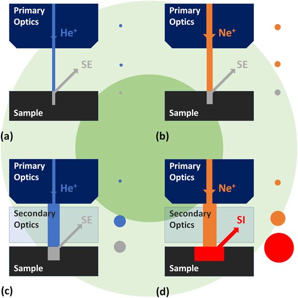
Because the high spatial resolution performance achievable with the NanoFab SIMS is not available on other systems, it is worthwhile to examine its performance and limiting factors in various operating modes. Figure 3 and Table 1 are intended to be read together to provide an overview of performance.

Figure 3: Semi-quantitative diagram highlighting the effects of the primary optics, secondary ion optics, and beam-sample interactions on the effective spot size for various operating modes of the instrument. Please refer to Table 1 and the article text for details and further explanation.
Table 1: Limits of spatial resolution for various instrument modes. Letters in the first column relate to the internal parts of Figure 3.

When using the instrument as a microscope (with the SIMS extractor retracted) to image the sample surface using the SE signal, the image resolution is < 1 nm (estimated from edge analysis) with a He+ primary beam. This represents the best condition for imaging the topography of the sample. The resolution is slightly worse (< 2 nm) when a neon beam is used. For both gases in imaging mode, the resolution is limited mainly by the primary optics (Figures 3a and 3b).
With the SIMS unit inserted and operated in negative mode, the He+ primary beam SE image resolution is ~4 nm using the total ion current (TIC) detector to record the SE signal (while simultaneously collecting a small negative secondary ion signal) (Figure 3c). This imaging mode is useful for taking a reference image prior to acquiring SIMS data. The degradation of resolution is caused by the effect of the electric field in the secondary ion extractor/deflector on the primary beam. This electric field is used to bend the secondary ion beam from the sample into the secondary ion transport optics. The Ne+ primary beam SE image resolution, with the SIMS unit inserted, is about 5 nm.
When using the Ne+ ion as the primary beam, with the SIMS extractor inserted and detecting either the total ion current or the mass-filtered secondary ion signal, the lateral spatial resolution limit is about 10 nm. In this case the main limiting factor is not the size of the primary beam, but the interaction of the beam with the sample (Figure 3d). Unlike secondary electrons, which originate from the area of the surface directly impacted by the ion beam [Reference Sijbrandij11], secondary ions can be generated and escape from areas of the sample surface that are several nanometers removed from the point of primary beam impact [Reference Wirtz8,Reference Wirtz, Hlawacek and Gölzhäuser9]. This 10 nm spatial resolution of analysis, limited primarily by beam-sample interactions, is unique to this instrument. The large green circles at the center of Figure 3 represent the primary beam size range (50–100 nm in diameter, depending on the ion source used) of current state-of-the-art instrumentation for high spatial resolution dynamic SIMS analysis [Reference Hoppe12], where the beam size clearly dominates the contribution of beam-sample interactions.
Accelerating voltage effects
In the above discussion, an acceleration voltage of 25 kV was implied, but it should be pointed out that this parameter influences performance as follows: the primary beam-size increases with decreasing acceleration voltage, while the width of the secondary-ion escape region decreases with acceleration voltage, so optimization requires a compromise. Operators have a range of 10 to 30 kV acceleration voltage available to optimize their experimental results for the material under analysis, in terms of effective spot size. The sputter rate typically does not vary dramatically for Ne+ irradiation over this voltage range, so effects on analysis time are not severe.
Analysis time
The analysis time depends mainly on the beam current used, typically 1–10 pA, and on data-acquisition settings such as pixel dwell-time, image size (total number of pixels in a map), and SIMS acquisition parameters. The latter include mass-range analyzed, dwell-time per analysis, and the number of scan-steps to acquire the mass spectrum. Typical acquisition times for a mass spectrum are 10 to 20 minutes. Typical acquisition times for chemical maps, using four ion detectors in parallel-detection mode, range between 10 minutes and 1 hour. For depth-profiling or 3-dimensional mapping, the analysis time depends strongly on the total volume of sample material removed and may range from several minutes to several hours, depending on the application.
Results
SIMS image resolution
Figure 4 shows results obtained from the well-established BAM-L200 certified reference sample [Reference Senoner13]. The NanoFab SIMS was used to map aluminum and gallium in the alternating GaAs and Al0.7Ga0.3As layers of the test sample. The finest details are in the form of line pairs of detected Al signal with a specified pitch (for example, P12 with 31 nm pitch) and solitary lines (for example, W11 with a narrow width). Figures 4b and 4c show an intensity line-profile taken through the aluminum map of the sample for certain line pairs (P9 through P14), with pitches from 76.5 nm to 17.5 nm, and these line-pairs were all clearly resolved. The profiles are suggestive of a single edge-resolution performance of about half the resolved pitch, say 10 nm, which is close to the beam-sample interaction limit. Note also that the system was sufficiently sensitive to image the solitary line W11 with a width of 3.5 nm.

Figure 4: Spatial resolution of analysis. (a) SIMS chemical map generated using the 27Al+ and 69Ga+ peaks from a BAM L-200 standard sample. (b) 27Al+ image showing analysis region across lines P9 to W11. (c) Image intensity profile taken from the sample region highlighted in (b). Line pairs P9 to P14 with pitches ranging from 76.5 nm to 17.5 nm, respectively, are resolved. Also detected was the narrow single line W11 (3.5 nm wide). A 10 keV Ne+ primary beam was used to generate these data.
Historical Metallurgy
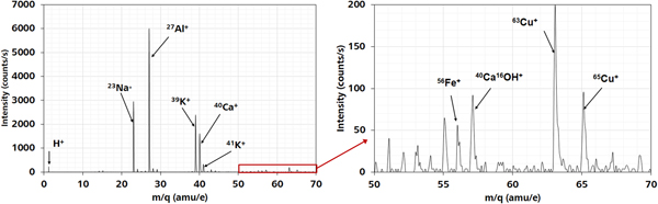
The specimen examined was an aluminum-copper alloy (with small amounts of iron and other elements) that was modeled after the alloy used in the 1903 Wright Flyer crankcase. The latter alloy, produced and applied before the formal discovery of precipitation hardening, can be considered the first aerospace aluminum alloy [Reference Gayle and Goodway14]. SE images, secondary ion mass spectra, and SIMS elemental maps were acquired with the NanoFab SIMS. Figure 5 shows a global mass spectrum from a flat-polished section of the alloy, with adjacent elements clearly separated (note the separation of 39K+ and 40Ca+). Figure 6 combines a SE image (in grayscale) with maps of 63Cu+ (blue) and 56Fe+ (red). This composite image highlights several features of the microstructure. Most of the sample consists of α-aluminum dendrites (grains), shown as the gray background provided by the SE signal. Note that there appears to be some iron, but not copper, in solid solution with aluminum. The copper map reveals the precipitate θ-Al2Cu in the boundaries between the dendrites. The iron map reveals some areas with finely structured iron-containing precipitates. Upon careful examination, needle-like ω-Al7Cu2Fe precipitates can be observed as features containing both copper and iron. The SE image also appears to reveal some other darker gray unidentified phases between and within the aluminum grains, thereby demonstrating the value of the multimodal imaging approach.

Figure 5: Mass spectrum from an aluminum-copper model alloy similar to the alloy used in the Wright Flyer crankcase. Elements detected related to aluminum alloy strengthening were Cu and Fe. Sample provided by Profs. Derk Joester and Kathleen Stair of the Material Science and Engineering Department, McCormick School of Engineering, Northwestern University, Evanston, IL.

Figure 6: Composite of elemental images from the model aluminum alloy similar to that found in the Wright Flyer crankcase. Composite was constructed by overlaying the iron and copper SIMS maps on the secondary electron (SE) image. Composite image shows copper-rich, iron-rich, and mixed-element precipitates (see text for details). Image width = 200 μm. Sample provided by Profs. Derk Joester and Kathleen Stair of the Material Science and Engineering Department, McCormick School of Engineering, Northwestern University, Evanston, IL.
Conclusion
An inert-gas focused ion beam tool and a custom magnetic-sector mass spectrometer have been combined, enabling both high-resolution (< 1nm) SE imaging and high spatial resolution (~10 nm) SIMS analysis and mapping within a single instrument. The SIMS resolution was demonstrated on a standard-resolution test sample. An example of multimodal analysis combining SE imaging and SIMS elemental maps was shown in a metallurgical study.
Acknowledgements
The authors thank Dr. Tom Wirtz and colleagues of the Luxembourg Institute of Science and Technology (LIST) and Dr. David Dowsett of Lion Nano-Systems for the long-standing collaborations that led to the development of the technology presented in this article. The authors thank Profs. Derk Joester and Kathleen Stair of Northwestern University for providing the sample of the aluminum-copper model alloy.