


Introduction
Recently, amorphous indium–gallium–zinc–oxide (a-IGZO) thin-film transistor (TFT) nonvolatile memories have been widely researched as next-generation memory devices for flexible electronics and transparent panel systems [Reference Iwasaki, Itagaki, Den, Kumomi, Nomura, Kamiya and Hosono1, Reference Jang, Park, Kong, Dong, Lee, Sohn, Cho and Kim2, Reference Suresh, Novak, Wellenius, Misra and Muth3, Reference Chen and Zan4]. This is because a-IGZO has many advantages over conventional amorphous or polycrystalline silicon, such as high electron mobility, good uniformity, low processing temperature, and visible light transparency [Reference Nomura, Kamiya, Yanagi, Ikenaga, Yang, Kobayashi, Hirano and Hosono5]. However, the a-IGZO TFT memory cannot be electrically erased by injecting holes into the charge storage layer from its channel, since a-IGZO is a natural n-type semiconductor and hole conduction is hard to generate under negative gate biasing [Reference Li, Pei, Hu, Chen, Ni, Lin, Zhang, Chen, Liang, Fan, Wang and Duan6, Reference Chen, Zhang, Cui, Sun and Zhang7, Reference Cui, Chen, Ding, Sun, Nyberg, Zhang and Zhang8]. Although light erasing [Reference Cui, Chen, Ding, Sun, Nyberg, Zhang and Zhang8, Reference Chen, Cui, Ding and Sun9] or light-assisted electrical erasing [Reference Chen, Zhang, Cui, Sun and Zhang7] was reported to improve the erasing efficiency of the devices, electrical erasure with a high efficiency is eagerly desired for a-IGZO TFT memory from the viewpoint of practical application. Recently, some researchers reported that the a-IGZO TFT memories with an IGZO or ZnO charge trapping layer (CTL) exhibited electrically erasable characteristics [Reference Yun, Kang and Yoon10, Reference Kim, Park, Yun, Lee, Kim and Yoon11, Reference Bak, Ryu, Park, Hwang and Yoon12]. However, most of them demonstrated an erasing bias as high as −20 V and a relatively long erasing time even up to 1 s [Reference Kim, Park, Yun, Lee, Kim and Yoon11, Reference Bak, Ryu, Park, Hwang and Yoon12]. Moreover, it was also reported that the a-IGZO TFT memory with an a-IGZO CTL could be erased under a gate bias of 12 V and a high drain bias of 10 V, a threshold voltage shift (ΔV th) of −3.88 V is obtained for an erasing duration of 10 ms [Reference Yin, Kim, Lim, Min, Kim, Song, Park, Kim, Tikhonovsky, Hyun and Park13]. All these practices will cause concerns about power consumption.
On the other hand, the demand for low-cost and high-density storage devices is pushing the physical scaling in charge trapping flash (CTF)-type memory devices. Thus, multilevel memory per cell is an urgent requirement in existing memory technology to increase the memory capacity without the need of stringent scaling. Furthermore, multi-functionalization of one device can improve circuit integration and reduce space occupation. In the past few years, synaptic devices that can emulate the signal transfer behaviors of the biological synapses have been paid more attention, which is ascribed to the necessity of the synaptic devices for building up the neuromorphic electronic systems [Reference Abbott and Regehr14, Reference Tian, Guo, Xie, Zhao, Li, Cha, Xia and Wang15]. Therefore, it is meritorious to explore whether the a-IGZO TFT device can realize both memory and synaptic functions.
In this article, a novel multilevel a-IGZO TFT memory cell is successfully demonstrated by using atomic layer–deposited Al2O3/ZnO/Al2O3 multilayers, where the ZnO layer acts as a CTL. In particular, the device exhibits a superior erasing efficiency under negative gate biasing. Moreover, the memory cell also demonstrates interesting synaptic behaviors.
Results and discussion
Figure 1 shows the programming and erasing characteristics of the a-IGZO TFT memory device under various gate biases. In terms of programming, the transfer curve moves gradually toward a positive bias as a function of programming voltage while keeping the programming time at 1 μs. The resulting ∆V th relative to the fresh device increased from 0.3 to 2.3 V as the programming voltage increased from 9 to 13 V, followed by a programming saturation, as shown in Fig. 1(a). The number of electrons captured by the CTL was calculated to be 8.5 × 10²²/cm2 according to Eq. (1) [Reference Li and Yang16]:
 $$Q = \mathop C\nolimits_{{\rm{ci}}} \Delta \mathop V\nolimits_{{\rm{th}}} \quad ,$$
where Q is the stored electron density captured by the CTL, ∆V th is the memory window, and C ci is the gate dielectric capacitance per unit area. Such a significant ΔV th suggests that considerable electrons from the n-type a-IGZO channel are injected into the ZnO CTL. Figure 1(b) shows the electrical erasing characteristics of the programmed device as a function of erasing voltage. As the erasing bias is enhanced from −9 to −13 V, the transfer curve shifts in the direction of a negative bias. After erasing at −13 V for 1 μs, a ∆V th as large as −7.4 V is achieved. The number of positive charge captured by the CTL was calculated to be 2.7 × 10²³/cm2. These results illustrate superior electrically erasable characteristics of the memory devices. Furthermore, an erasing saturation also appears when the erasing bias increases to −12 V.

Figure 1: (a) The programming characteristics of the a-IGZO TFT memory device under various positive gate biases. (b) The erasing characteristics of the programmed device under various negative gate biases.
Figure 2 shows dependence of the readout drain current (I DS) of the memory on pulse width under programming and erasing modes. In terms of programming at 13 V, the programmed device exhibits a small I DS (i.e., less than 1 × 10⁻¹¹ A) when the gate bias is zero. This is because the trapped electrons in the CTL repel electrons in the channel, thus reducing the electron concentration in the channel. With respect to erasing at −8 V, the erased device shows a large I DS (i.e., larger than 1 × 10⁻⁸ A) when the gate bias is zero. This should be attributed to the trapped positive charges in the CTL, which induces additional electrons in the channel, hence increasing the electron concentration in the channel. Therefore, the former is defined as an OFF state, corresponding to a programmed device, and the latter is defined as an ON state, corresponding to an erased device. Furthermore, as the pulse width increases from 1 × 10⁻⁶ to 5 × 10⁻³ s, the I DS in the OFF state does not show an evident variation trend. However, the I DS in the ON state demonstrates a gradual increase with the pulse width, i.e., I DS rises from 2 × 10⁻⁸ to 6.5 × 10⁻⁷ A with increasing the pulse width from 1 × 10⁻⁶ to 5 × 10⁻³ s. That is, the ON/OFF I DS ratio increases from ∼104 to ∼106, which means an increasing memory window as a function of pulse width. Furthermore, the inset in Fig. 2 indicates that the memory device can be easily switched between the programmed state and erased state, demonstrating a large memory window of 3 V after 13 V/1 μs programming and −8 V/2 μs erasing.

Figure 2: Variations of I DS as a function of pulse width for the memory devices in ON and OFF states. The programming voltage corresponding to the OFF state was fixed at 13 V, and the erasing voltage corresponding to the ON state was kept at −8 V. The inset shows the successive programming and erasing characteristics of the device.
Figure 3 shows the memory retention characteristics by monitoring time-dependent I DS in the ON and OFF states. In terms of 13 V/1 μs programming and −12 V/1 µs erasing, the ON/OFF I DS ratio still remains ∼103 after 105 s. Figure 4 shows the endurance characteristics of the memory as a function of P/E cycles. In the case of the above-mentioned P/E conditions, the device exhibits a stable and large memory window, i.e., the ON/OFF I DS ratio is as large as ∼106 till 104 of P/E cycles. Table I compares the erasing characteristics of various reported a-IGZO TFT memories and the current device. It is found that our device exhibits a much higher erasing efficiency under a low bias (−12 V) and a short time (1 μs).

Figure 3: Dependence of I DS on time for the memory devices in the ON and OFF states, which were obtained by applying −12 V/1 μs and 13 V/1 μs pulses to the gate, respectively. The I DS was measured under V GS = 0 V and V DS = 0.1 V at room temperature.

Figure 4: Variations of I DS as a function of P/E cycles for the memory device. The P and E conditions correspond to 13 V/1 μs and −12 V/1 μs, respectively. The readout drain current (I DS) was measured under V GS = 0 V and V DS = 0.1 V at room temperature.
TABLE I: Comparison of the ON/OFF of various a-IGZO TFT memories with different gate stacks.

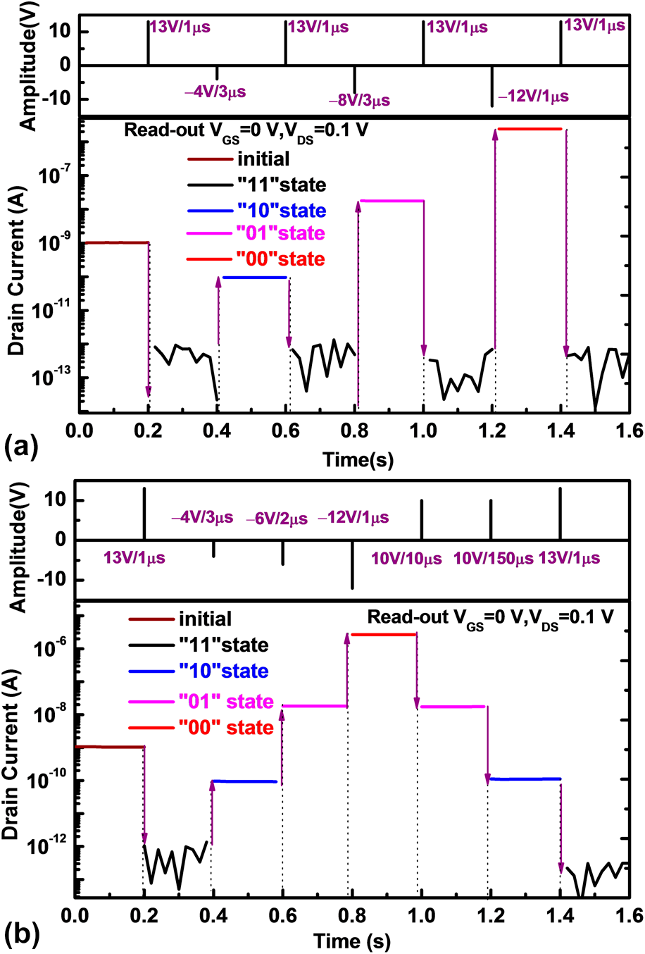
A multilevel memory cell is also demonstrated for the devices, as shown in Fig. 5(a). After programming at 13 V for 1 µs, the fresh device becomes the “11” state corresponding to an I DS of ∼1 × 10⁻¹² A. Subsequently, the device is erased at −4 V for 3 µs and becomes the “10” state corresponding to an I DS of ∼1 × 10⁻¹⁰ A. When the erased device is reprogrammed at 13 V for 1 µs, it recovers to the “11” state again. If the erasing bias is enhanced to −8 V, the resulting I DS increases to 2 × 10⁻⁸ A for 3 µs of erasing time, defined as “01” state. If the erasing bias is enhanced to −12 V, the I DS increases to 2 × 10⁻⁶ A for 1 µs erasing time, labeled as the “00” state. Therefore, four states per cell with an enough large I DS ratio (≥∼102) between any two states are achieved by adjusting erasing conditions. Furthermore, continuous switching among these states is also illustrated in Fig. 5(b). The memory device can be switched from “11” → “10” → “01” → “00” state, and vice versa. For example, the “11” state is switched to the “10” state after erasing at −4 V for 3 µs. Following erasing at −6 V for 2 µs, the “10” state can be further switched to the “01” state. It is worth mentioning that the I DS corresponding to different states can be modulated by well-engineering programming and erasing operations to achieve desired current levels to detect different electrical memory states.

Figure 5: The multilevel memory performance of the devices: (a) mutual switching between “11” and “10”, “11” and “01”, and “11” and “00,” respectively; (b) continuous switching from “11” → “10” → “01” → “00”, and vice versa.
Recently, synaptic devices have attracted much attention because of their potentials in neuromorphic electronic systems. Therefore, it is of significance to explore whether the a-IGZO TFT memory can be used for synaptic transistors, especially under different memory states. To investigate the synapse-emulating behaviors of the a-IGZO TFT memory, a presynaptic spike needs to be applied to the bottom gate of the device while the drain current of the device is measured as a function of time at some source-drain voltage (V ds). Thus, the resulting drain current is defined as an inhibitory postsynaptic current (IPSC). Similarly, if a negative presynaptic spike (−3 V/20 ms) is applied to the back gate, the resulting drain current is defined as an excitatory postsynaptic current (EPSC). Figures 6(a) and 6(b) show the typical IPSC and EPSC of the memory device associated with “10” state in response to presynaptic spikes of 3 V/20 ms and −3 V/20 ms, respectively, at V ds = 50 mV. In general, the interface traps between the a-IGZO channel and the Al2O3 gate dielectric can capture electrons under a positive presynaptic spike, and this leads to a decrease in the drain current. After removal of the spike, the captured electrons are gradually de-trapped, hence resulting in a gradual recovery of IPSC toward the initial drain current, as indicated in Fig. 6(a). Furthermore, it is reported that neutral oxygen vacancies in a-IGZO act as shallow donors, and under a negative gate bias, some neutral oxygen vacancies (V O) in the a-IGZO channel become positively charged due to lowering of the Fermi level for electrons (E F) at the surface of the a-IGZO channel [Reference Noh, Chang, Ryu and Lee20]. Thus, the negative presynaptic spike can give rise to accumulation of positively charged oxygen vacancies at the a-IGZO/Al2O3 interface, thus increasing the drain current, as shown in Fig. 6(b). After the negative spike, the resulting EPSC exhibits very small attenuation. This could be attributed to low-speed departure of positively charged oxygen vacancies from the interface. In the current experiment, it is much interesting to find that both the IPSC and EPSC curves of the devices exhibit obvious difference for different memory states, as shown in Figs. 6(c) and 6(d). As the memory state changes from “11” → “10” → “01” → “00”, both the normalized IPSC and EPSC decrease gradually. This should be related to the amount and type of charges trapped in the ZnO layer under different memory state, which further interact with the presynaptic spike, finally determining the electron concentration in the channel. In a word, the a-IGZO TFT memory successfully demonstrates the emulation of synaptic behaviors and exhibits tunable EPSC/IPSC properties along with various memory states.

Figure 6: (a) Typical IPSC curve recorded from the memory device corresponding to “10” state in response to one positive presynaptic spike (3 V/20 ms); (b) typical EPSC curve recorded from the memory device corresponding to “10” state in response to one negative pre-synaptic spike (−3 V/20 ms); (c) normalized IPSC (−ΔI IPSC/I initial) for different memory state; and (d) normalized EPSC (ΔI EPSC/I initial) for different memory states.
Conclusion
The multilevel a-IGZO TFT memory cell is achieved by using atomic layer deposition (ALD) ZnO as a CTL. The device shows a much higher erasing efficiency at a negative bias, as compared with conventional a-IGZO TFT-based memories, which exhibited poor erasing characteristics. The device exhibits good endurance and promising retention characteristics. Additionally, typical synaptic behaviors including EPSC and IPSC with different memory times at different memory states were also successfully demonstrated.
Methods
A cleaned p-type Si(100) wafer (ρ = 0.001–0.005 Ω cm) was used as the starting substrate, which served as the back gate of the device. Then, multilayers of Al2O3 (35 nm)/ZnO (20 nm)/Al2O3 (8 nm) were successively deposited by ALD, which were used as the blocking layer, CTL, and tunneling layer, respectively. Herein, the precursors for ALD Al2O3 and ZnO films were Al(CH3)3/H2O and Zn(C2H5)2/H2O, respectively. After that, a 40 nm a-IGZO film was deposited by radio frequency magnetron sputtering at room temperature using an InGaZnO4 target under the conditions, i.e., Ar = 50 sccm, power = 110 W, and working pressure = 0.87 Pa. Subsequently, the active channel was defined by photolithograph and wet etch, and then 30 nm Ti/70 nm Au bilayer electrodes were formed by e-beam evaporation and lift-off technique. Finally, the fabricated device was annealed at 250 °C in O2 for 5 min.
Electrical measurements were performed on the devices with a channel length (L = 10 μm)/width (W = 60 μm) using a semiconductor device analyzer (Agilent B1500A) at room temperature.
Acknowledgments
The authors would like to acknowledge the financial support in part by the National Natural Science Foundation of China (Grant No. 61874029), and in part by the National Key Technologies Research and Development Program of China (Grant No. 2015ZX02102-003).


