


Introduction
The channeling dependence of the electron backscatter yield in a scanning electron microscope (SEM) is exploited in techniques such as electron backscatter diffraction (EBSD) and electron channeling contrast imaging (ECCI). EBSD provides information on crystal phases, their orientation, grain boundaries, and strain (Zaefferer, Reference Zaefferer2007; Schwartz et al., Reference Schwartz, Kumar, Adams and Field2009), while ECCI is used for imaging crystal defects such as dislocations, stacking faults, and subgrain boundaries (Wilkinson & Hirsch, Reference Wilkinson and Hirsch1997; Zaefferer & Elhami, Reference Zaefferer and Elhami2014). Simulations are often essential for interpreting subtle features in the data, such as ferroelectric domains (Burch et al., Reference Burch, Fancher, Patala, De Graef and Dickey2017), chirality (Winkelmann & Nolze, Reference Winkelmann and Nolze2015), and strain (Britton et al., Reference Britton, Maurice, Fortunier, Driver, Day, Meaden, Dingley, Mingard and Wilkinson2010) in EBSD, as well as the contrast due to elastic strain fields in ECCI (Picard et al., Reference Picard, Liu, Lammatao, Kamaladasa and De Graef2014; Kriaa et al., Reference Kriaa, Guitton and Maloufi2019). While there have been several attempts at modeling electron backscattering under channeling conditions (Spencer et al., Reference Spencer, Humphreys and Hirsch1972; Dudarev et al., Reference Dudarev, Rez and Whelan1995), current Bloch wave-based simulation methods (Winkelmann et al., Reference Winkelmann, Trager-Cowan, Sweeney, Day and Parbrook2007; Winkelmann, Reference Winkelmann2008, Reference Winkelmann2009; Callahan & De Graef, Reference Callahan and De Graef2013; Picard et al., Reference Picard, Liu, Lammatao, Kamaladasa and De Graef2014; Pascal et al., Reference Pascal, Singh, Callahan, Hourahine, Trager-Cowan and De Graef2018) rely on the observation that electron backscattering is largely incoherent, so that the backscatter signal from any given atom is proportional to the local electron beam intensity. Furthermore, in EBSD the reciprocity principle (Winkelmann, Reference Winkelmann2008) is invoked to simplify calculation of the backscattered wave propagation toward the detector, while in ECCI the column approximation (Hirsch et al., Reference Hirsch, Howie, Nicholson, Pashley and Whelan1965) is assumed so that Bloch waves can be applied to a defect crystal in a tractable manner.
An important feature of Bloch wave calculations is that inelastic scattering is modeled phenomenologically via a complex crystal potential (Hirsch et al., Reference Hirsch, Howie, Nicholson, Pashley and Whelan1965). The imaginary term of the potential results in an electron flux that is continuously depleted as the electron beam propagates through the crystal. Since the exact distribution of the diffuse scattered intensity within the specimen is unknown, it is difficult to accurately calculate its contribution to the backscattered signal. On the other hand, the physical optics-based multislice method (Cowley & Moodie, Reference Cowley and Moodie1957; Kirkland, Reference Kirkland2010), using either the (quasi-elastic) frozen phonon model (Loane et al., Reference Loane, Xu and Silcox1991) or the quantum excitation of phonons model (Forbes et al., Reference Forbes, Martin, Findlay, D'Alfonso and Allen2010; Forbes & Allen, Reference Forbes and Allen2016), can reproduce the diffuse scattered intensity distribution due to phonon scattering. This is essential for correctly modeling the intensity of Kikuchi bands and higher-order Laue zone (HOLZ) rings (Kirkland, Reference Kirkland2010). Chen & Van Dyck (Reference Chen and Van Dyck1997) developed a more accurate multislice method that is applicable to the lower electron beam energies in an SEM. For reasons that will be discussed later (see "Methods" section), this produces better agreement with experimental EBSD patterns compared to the conventional, high-energy multislice calculations (Liu et al., Reference Liu, Cai, Zhou and Wang2016).
Apart from phonon losses, the incident electron can also scatter inelastically through collective plasmon excitations as well as single electron ionization and interband transition events. Of these, plasmons typically have the largest scattering cross-section (Egerton, Reference Egerton1996). Energy-filtered EBSD patterns have shown that for the standard experimental geometry of a 70° tilted sample, the Kikuchi band contrast first increases with energy loss, reaching maximum contrast at few tens or hundreds of eV, before slowly decreasing at higher energy losses (Deal et al., Reference Deal, Hooghan and Eades2008; Vos & Winkelmann, Reference Vos and Winkelmann2019). The energy loss at peak contrast is well below that of single electron ionization but greater than the recoil energy for backscattering (Winkelmann & Vos, Reference Winkelmann and Vos2013), which suggests that the contrast mechanism may also involve plasmon and/or interband transitions. Therefore, accurate simulation of EBSD patterns requires at least plasmon scattering to be included alongside phonons. To our knowledge, there are no reports of energy-filtered ECCI images, although the introduction of Timepix direct electron detectors with energy thresholding (Vespucci et al., Reference Vespucci, Winkelmann, Naresh-Kumar, Mingard, Maneuski, Edwards, Day, O'Shea and Trager-Cowan2015) may make acquiring such images possible.
Recently, Monte Carlo methods have been used to include plasmon excitations in multislice simulations (Mendis, Reference Mendis2019, Reference Mendis2020; Barthel et al., Reference Barthel, Cattaneo, Mendis, Findlay and Allen2020). The underlying principle is that plasmon excitations are highly delocalized (Muller & Silcox, Reference Muller and Silcox1995) and are, therefore, not significantly affected by electron beam channeling. Computer-generated random numbers are used to estimate the plasmon scattering depth and angle. The depth is sampled from a Poisson distribution with the mean value equal to the plasmon mean free path, while the angle is sampled from a Lorentzian distribution with half-width-at-half-maximum equal to the plasmon characteristic scattering angle (Egerton, Reference Egerton1996). Following plasmon excitation at the estimated depth, the estimated scattering angle is used to modify the subsequent electron trajectory through the sample (the change in electron wavelength due to plasmon energy loss is often sufficiently small to be neglected). This process is repeated for many plasmon “configurations” and the results incoherently summed to give a statistically averaged result. Plasmon multislice simulations have been shown to reproduce experimental energy-filtered diffraction patterns (Mendis, Reference Mendis2019), as well as the angular distribution of scattering in position averaged convergent beam electron diffraction (PACBED) patterns (Barthel et al., Reference Barthel, Cattaneo, Mendis, Findlay and Allen2020). These calculations were, however, for high-energy electron diffraction in transmission geometry.
In this paper, we introduce plasmon excitations to the multislice method of Chen & Van Dyck (Reference Chen and Van Dyck1997) with the purpose of uncovering their role in the contrast mechanisms in EBSD and ECCI. This is an improvement over current simulation methods (Winkelmann et al., Reference Winkelmann, Trager-Cowan, Sweeney, Day and Parbrook2007; Winkelmann, Reference Winkelmann2008, Reference Winkelmann2009; Callahan & De Graef, Reference Callahan and De Graef2013; Picard et al., Reference Picard, Liu, Lammatao, Kamaladasa and De Graef2014; Pascal et al., Reference Pascal, Singh, Callahan, Hourahine, Trager-Cowan and De Graef2018) which assume no inelastic scattering (apart from phonons) before or after the backscattering event in ECCI and EBSD, respectively. The energy of backscattered electrons can vary over all energies up to the primary energy of the incident electron beam. However, much of the channeling contrast signal is contained in those electrons with low energy loss (Deal et al., Reference Deal, Hooghan and Eades2008; Vos & Winkelmann, Reference Vos and Winkelmann2019), while the higher energy-loss electrons contribute a background signal with no useful information. While our simulations cannot reproduce the full energy spectrum of the backscattered electrons, it does offer insight into the underlying scattering mechanisms that govern channeling contrast. It could also be useful for quantitative comparison with energy-filtered data or for estimating the optimum experimental conditions for a given measurement.
Methods
Multislice Method
The conventional multislice method, first proposed by Cowley & Moodie (Reference Cowley and Moodie1957), is based on an approximate form of the Schrödinger equation, where the second derivative of the electron wavefunction Ψ with respect to depth z (i.e., the ∂ 2Ψ/∂z 2 term) is assumed to be small (Kirkland, Reference Kirkland2010). This approximation is valid at high energies ( ${\rm \gtrsim }$100 keV) of the incident electron beam since then scattering is weak and the wavefunction changes only slowly as a function of depth within the specimen. For sufficiently small slice thickness, the error is O(λ 3), where λ is the incident electron wavelength (Chen & Van Dyck, Reference Chen and Van Dyck1997). For lower beam energies (e.g., SEM) the more accurate multislice method of Chen & Van Dyck (Reference Chen and Van Dyck1997), based on the full Schrödinger equation, may be required. For example, at lower energies, the electron refractive index will depend on higher-order terms in the specimen potential (Lentzen, Reference Lentzen2017); this limits the accuracy of the phase grating function as used in the conventional multislice model, where the phase shift due to scattering is taken to be proportional to the slice potential (Kirkland, Reference Kirkland2010). Similarly, the higher scattering angles at lower energies may mean that the parabolic approximation assumed for the Ewald sphere propagator function is no longer valid (Ming & Chen, Reference Ming and Chen2013). A further benefit of the Chen and Van Dyck method is that it is also accurate for large beam tilts (Chen et al., Reference Chen, Van Dyck and Op de Beeck1997). This is particularly important for the EBSD simulations in this work, where the beam tilt is as large as 30° (see "Methods" section). For these reasons we use the more accurate multislice method of Chen & Van Dyck (Reference Chen and Van Dyck1997) for the simulations, the implementation of which is summarized below.
In multislice, the specimen is divided into a series of thin slices of thickness ε in the z-direction. The full Schrödinger equation for the jth-slice, which extends from z = (j − 1)ε to z = jε, can be expressed as follows (Chen & Van Dyck, Reference Chen and Van Dyck1997):
 $$\displaystyle{{\partial ^2{\Psi }^j\lpar {\mathbf{\bf r}} \rpar } \over {\partial z^2}} + \lsqb {2\pi {\hat{k}}_j\lpar {\mathbf{\bf R}} \rpar } \rsqb ^2{\Psi }^j\lpar {\mathbf{\bf r}} \rpar = 0,$$
 $$\hat{k}_j\lpar {\mathbf{\bf R}} \rpar = K_{\rm o}\sqrt {1 + \displaystyle{{\nabla _{xy}^2 } \over {{\lpar {2\pi K_{\rm o}} \rpar }^2}} + \displaystyle{\sigma \over {\pi K_{\rm o}}}U_j\lpar {\mathbf{\bf R}} \rpar }, $$
 $$U_j\lpar {\mathbf{\bf R}} \rpar = \displaystyle{1 \over \varepsilon }\int_{\lpar {\,j-1} \rpar \varepsilon }^{\,j\varepsilon } {U\lpar {\mathbf{\bf r}} \rpar {d}z}, $$
where Ψj(r) is the electron wavefunction for the jth-slice at the position vector r = (R, z), with R being a two-dimensional position vector in the xy-plane of the specimen. K o is the wavenumber of the incident electron,  $\nabla _{xy}^2 = \lpar \partial ^2/\partial x^2\rpar + \lpar \partial ^2/\partial y^2\rpar \;$ is the Laplacian in the xy-plane and σ = 2πem/(K oh 2) is the interaction constant (e and m are the charge and mass of the electron and h is Planck's constant). Uj(R) is the slice potential U(r) projected along the z-direction. The $\hat{k}_j\lpar {\mathbf{\bf R}} \rpar \;$operator is valid for scattering in the forward direction (Chen & Van Dyck, Reference Chen and Van Dyck1997). Note that equation (1a) includes the ∂ 2Ψj/∂z 2 term which is required for higher accuracy.
By use of suitable boundary conditions (i.e., Ψj and ∂Ψj/∂z are continuous at the boundary between neighboring slices), the forward scattered wave can be calculated using a so-called transfer matrix method; see Chen & Van Dyck (Reference Chen and Van Dyck1997) for details. For materials where backscattering is negligible (e.g., light atomic number elements such as silicon), it can be shown that the forward scattered wave Ψm for the mth-slice is given by the following equation (Chen & Van Dyck, Reference Chen and Van Dyck1997):
 $${\Psi }^m = \left({\mathop \prod \limits_{\,j = 1}^{m-1} e^{2\pi i{\hat{k}}_j\varepsilon }} \right){\Psi }_p, $$
with Ψp being the incident wavefunction at the specimen entrance surface. The exponential operator in equation (2) represents evolution of the wavefunction as it propagates between neighboring slices. It has been shown that a second-order expansion of the operator is sufficient for accurate simulation of EBSD patterns under SEM beam voltages (Liu et al., Reference Liu, Cai, Zhou and Wang2016). Expanding equation (1b) to second order:
 $$\eqalign{{\hat{k}}_j& = K_{\rm o} + \displaystyle{{\nabla _{xy}^2 } \over {8\pi ^2K_{\rm o}}}-\displaystyle{{\nabla _{xy}^4 } \over {128\pi ^4K_{\rm o}^3 }} + \displaystyle{{\sigma U_j} \over {2\pi }}\left({1-\displaystyle{{\sigma U_j} \over {4\pi K_{\rm o}}}} \right)\cr & \;-\sigma \left({\displaystyle{{\nabla_{xy}^2 U_j + U_j\nabla_{xy}^2 } \over {32\pi^3K_{\rm o}^2 }}} \right)-\displaystyle{1 \over {64\pi ^4K_{\rm o}^3 }}\displaystyle{{\partial ^4} \over {\partial x^2\partial y^2}}} $$
and so:
 $$e^{2\pi i\lpar {{\hat{k}}_j-K_{\rm o}} \rpar \varepsilon }\approx o\lpar {\mathbf{\bf R}} \rpar p_2\lpar {\mathbf{\bf R}} \rpar p_1\lpar {\mathbf{\bf R}} \rpar q\lpar {\mathbf{\bf R}} \rpar, $$
 $$q\lpar {\mathbf{\bf R}} \rpar = {\rm exp}\left[{i\sigma U_j\varepsilon \left({1-\displaystyle{{\sigma U_j} \over {4\pi K_{\rm o}}}} \right)} \right],$$
 $$p_1\lpar {\mathbf{\bf R}} \rpar = {\rm exp}\left({i\varepsilon \displaystyle{{\nabla_{xy}^2 } \over {4\pi K_{\rm o}}}} \right)\quad {\rm and} \quad p_2\lpar {\mathbf{\bf R}} \rpar = {\rm exp}\left({-i\varepsilon \displaystyle{{\nabla_{xy}^4 } \over {64\pi^3K_{\rm o}^3 }}} \right),$$
 $$\eqalign{o\lpar {\mathbf{\bf R}} \rpar & = {\rm exp}\left[{-i\varepsilon \left({\sigma \displaystyle{{\nabla_{xy}^2 U_j + U_j\nabla_{xy}^2 } \over {16\pi^2K_{\rm o}^2 }} + \displaystyle{1 \over {32\pi^3K_{\rm o}^3 }}\displaystyle{{\partial^4} \over {\partial x^2\partial y^2}}} \right)} \right]\cr & \;\approx {\rm exp}\left[{-i\varepsilon \sigma \left({\displaystyle{{\nabla_{xy}^2 U_j + U_j\nabla_{xy}^2 } \over {16\pi^2K_{\rm o}^2 }}} \right)} \right],} $$
where  $\nabla _{xy}^4 = \lpar \partial ^4/\partial x^4\rpar + \lpar \partial ^4/\partial y^4\rpar.$ In equation (3b), a constant phase term exp(−2πiK oε) has been included to simplify the operator expansion (Chen & Van Dyck, Reference Chen and Van Dyck1997), but which otherwise has no effect on the calculated beam intensities. q(R) is a modified phase grating function, p 1(R) is the standard propagator function in conventional multislice (Kirkland, Reference Kirkland2010) and p 2(R) is a higher-order propagator function. The propagator functions represent a convolution in real space and are therefore more efficiently calculated in reciprocal space (Kirkland, Reference Kirkland2010). The Fourier transforms (FT) are given by the following equations (see Kirkland (Reference Kirkland2010) for a derivation for p 1(R); the result for p 2(R) follows similar lines):
 $${\rm FT}\lcub {\,p_1\lpar {\mathbf{\bf R}} \rpar } \rcub = {\exp}\lpar {-i\pi \lambda \varepsilon k^2} \rpar \quad {\rm and }\quad {\rm FT} \lcub {\,p_2\lpar {\mathbf{\bf R}} \rpar } \rcub = {\exp}\left[{-\displaystyle{{i\pi \lambda^3\varepsilon } \over 4}\lpar {k_x^4 + k_y^4 } \rpar } \right],$$
where k = (kx,ky) is a reciprocal space vector. Equation (3b) follows from equation (3a) and makes use of the general expansion exp(A + B) = exp(A)exp(B), which is only true if the two operators A and B commute, that is, AB = BA (Kirkland, Reference Kirkland2010). The commutative property is, however, not valid for the phase grating function q(R) and propagator functions p 1(R), p 2(R), so that equation (3b) is only valid to first order (Kirkland, Reference Kirkland2010). The so-called mixed operator o(R) represents propagation of the electron beam within the specimen potential (as opposed to free space). It does not have a simple Fourier transform and must, therefore, be evaluated in real space. For the simulations on silicon in this work, it is found that o(R) does not have a significant effect on the results, although its effect may be more important for specimens of higher atomic number (Ming & Chen, Reference Ming and Chen2013). If o(R) is neglected, the multislice simulations can be performed using Fast Fourier Transforms, which is computationally more efficient than real space calculation of the  ${\rm exp}\lsqb {2\pi i\lpar {\hat{k}}_j-K_{\rm o}\rpar \varepsilon } \rsqb$ operator used previously (Cai & Chen, Reference Cai and Chen2012; Spiegelberg & Rusz, Reference Spiegelberg and Rusz2015; Liu et al., Reference Liu, Cai, Zhou and Wang2016). Nevertheless, in this work, o(R) was included for completeness; it was expanded up to second order and evaluated in real space. In order to reduce aliasing artifacts during convolution the bandwidth of q(R), p 1(R), and p 2(R) are limited to two-thirds the Nyquist limit, similar to conventional multislice simulations (Kirkland, Reference Kirkland2010).
For EBSD and ECCI simulations, we are interested in the backscattered electron intensity, which is dominated by high-angle thermal diffuse scattering (Winkelmann et al., Reference Winkelmann, Trager-Cowan, Sweeney, Day and Parbrook2007; Winkelmann, Reference Winkelmann2009). This is easily seen for scattering by a single atom, where the elastic and thermal diffuse scattered (TDS) intensities for scattering vector q are proportional to |f(q)|2exp(−2Bq 2) and |f(q)|2[1−exp(−2Bq 2)], respectively, with f(q) being the atom scattering factor and B the Debye–Waller factor. At sufficiently large q, the TDS contribution becomes greater than the elastic scattering (Pennycook & Jesson, Reference Pennycook and Jesson1991). As an example, for silicon at 5 kV (the simulation conditions in this paper), the cross-over point is at 12°, which is well below the minimum angle of 20° required for backscattering in a standard EBSD measurement with 70° beam incidence angle. As further evidence for the dominance of TDS scattering in a crystal, we have used the Chen & Van Dyck (Reference Chen and Van Dyck1997) multislice method to simulate the purely elastic backscattered diffraction pattern for [001]-silicon. The simulated results are presented in the Appendix and appear very different to experimental EBSD patterns, thereby confirming that TDS is the dominant mechanism responsible for backscattering.
In the incoherent limit (i.e., large collection solid angle), the TDS inelastic scattered intensity is proportional to (Lugg et al., Reference Lugg, Neish, Findlay and Allen2014)
 $$\int {\left\{{\mathop \sum \limits_n {\vert {{\Psi }_n\lpar {\mathbf{\bf r}} \rpar } \vert }^2} \right\}V\lpar {\mathbf{\bf r}} \rpar {d}{\mathbf{\bf r}}}, $$
where V(r) is the interaction potential and Ψn(r) is the electron wavefunction with the specimen in the nth-phonon configuration. Equation (5) is integrated over the entire analytical volume. For backscattering, the TDS interaction potential is well approximated by a delta function centered on each atom (Rossouw et al., Reference Rossouw, Miller, Josefsson and Allen1994), so that the TDS backscattered signal from a given atom is proportional to the local electron beam intensity [i.e., the summation term within the curly brackets in equation (5)]. The electron beam intensity can be calculated using equation (2) alongside a quantum excitation of phonons model (Forbes et al., Reference Forbes, Martin, Findlay, D'Alfonso and Allen2010; Forbes & Allen, Reference Forbes and Allen2016) for the different phonon configurations.
Plasmon Excitations
In this section, the Monte Carlo method for simulating plasmon excitations is summarized. The plasmon scattering depth (s), polar (θ), and azimuthal (ϕ) scattering angles are estimated using the following formulas (Mendis, Reference Mendis2019; Barthel et al., Reference Barthel, Cattaneo, Mendis, Findlay and Allen2020):
 $$s = {-}\lambda _{\rm p}{\ln}\lpar {R_1} \rpar, $$
 $$\theta = \theta _{\rm E}\sqrt {{\left({\displaystyle{{\theta_{\rm c}^2 + \theta_{\rm E}^2 } \over {\theta_{\rm E}^2 }}} \right)}^{R_2}-1}, $$
 $$\phi = 2\pi R_3,$$
where R 1, R 2, and R 3 are computer-generated linear random variables within the range [0,1], λ p is the plasmon mean free path, and θ E and θ c are the characteristic and critical plasmon scattering angles, respectively (Egerton, Reference Egerton1996). θ E can be calculated from E p/(2E o), where E p is the plasmon energy [17 eV for silicon (Mendis, Reference Mendis2019)] and E o is the primary beam energy. Barthel et al. (Reference Barthel, Cattaneo, Mendis, Findlay and Allen2020) obtained values of λ p = 1000 Å and θ c = 15 mrad by fitting simulations to experimental PACBED patterns of [110]-Si at 300 kV. Extrapolating to 5 kV, the beam voltage used for the present simulations, we obtain λ p = 16.7 Å and θ c = 132 mrad. These values are derived from the fact that λ p is approximately proportional to E o and that the critical scattering vector magnitude q = sin(θ c)/λ is independent of E o (Egerton, Reference Egerton1996).
Following propagation of the electron beam to a depth s within the sample, the scattering angles θ and ϕ due to plasmon excitation modify the subsequent electron trajectory. The wavefunction must, therefore, be multiplied by a phase ramp term, exp(2πiΔkt⋅R), where Δkt is the change in transverse wavevector due to plasmon scattering (Barthel et al., Reference Barthel, Cattaneo, Mendis, Findlay and Allen2020). This method has been shown to accurately reproduce the angular distribution of scattering in PACBED patterns (Barthel et al., Reference Barthel, Cattaneo, Mendis, Findlay and Allen2020). A similar approach is, therefore, adopted here, that is, at the slice m where plasmon scattering takes place the wavefunction Ψm [equation (2)] is multiplied by exp(2πiΔkt⋅R). Δkt is rounded to the nearest pixel of the multislice supercell in reciprocal space, to comply with the periodic boundary conditions of the simulation and avoid aliasing artifacts (Barthel et al., Reference Barthel, Cattaneo, Mendis, Findlay and Allen2020). The large θ c value of 132 mrad at 5 kV can also pose problems with the available bandwidth for the multislice supercell, especially when multiple scattering is involved. To mitigate this, an upper θ limit of 50θ E (i.e., 85 mrad or nearly twice the {220} Bragg angle) is imposed. This does not lead to a significant error since the cross-section at a scattering angle of θ = 50θ E is smaller by four orders of magnitude compared to forward scattering. Implementation of plasmon excitations is computationally more efficient in multislice compared to Bloch waves since for the latter the Bloch wave coefficients and excitations must be re-calculated after each plasmon event, which is more time-consuming. However, in all cases, inclusion of plasmons increases the overall simulation time compared to standard calculations for elastic and phonon scattering only.
EBSD and ECCI Simulations
EBSD and ECCI simulations are carried out on a [001]-silicon specimen using a 5 kV electron beam. 5 kV, rather than a higher beam voltage, was selected in order to achieve a reasonable computation time for the EBSD simulations. The shorter plasmon mean free path at 5 kV requires a smaller supercell thickness for examining the role of multiple plasmon scattering on EBSD contrast. Kirkland's atom scattering factors (Kirkland, Reference Kirkland2010) were used to calculate the projected potential of the supercell slices. The quantum excitation of phonons model (Forbes et al., Reference Forbes, Martin, Findlay, D'Alfonso and Allen2010; Forbes & Allen, Reference Forbes and Allen2016), with 0.078 Å root-mean-square uncorrelated atom displacement (Kirkland, Reference Kirkland2010), is used to model phonon scattering. Plasmon excitations are simulated using the method described previously. In all simulations, only the TDS backscattered signal is calculated via equation (5) and assuming a delta function interaction potential (Rossouw et al., Reference Rossouw, Miller, Josefsson and Allen1994). The TDS backscattered signal is, therefore, proportional to the local electron beam intensity [i.e., |Ψm|2 in equation (2)] at the backscattering atom (Winkelmann et al., Reference Winkelmann, Trager-Cowan, Sweeney, Day and Parbrook2007; Winkelmann, Reference Winkelmann2008, Reference Winkelmann2009; Callahan & De Graef, Reference Callahan and De Graef2013; Picard et al., Reference Picard, Liu, Lammatao, Kamaladasa and De Graef2014; Pascal et al., Reference Pascal, Singh, Callahan, Hourahine, Trager-Cowan and De Graef2018).
EBSD calculations are based on the principle of reciprocity (Winkelmann, Reference Winkelmann2008). As illustrated schematically in Figure 1a, backscattering from an atom “P” can take place in many directions, but only those multiple scattered electrons that exit the sample in the direction of the EBSD camera will be detected. Each pixel in the (far-field) EBSD camera corresponds to backscattered electrons that share a common wavevector. By reciprocity, the backscattered signal from atom “P” is, therefore, proportional to the local electron beam intensity at “P” with the EBSD detector pixel as the source, which is in the far-field and therefore effectively corresponds to an incident plane wave with wavevector along the direction from pixel to sample. Strictly speaking, the backscattered signal must also include a weighting term due to the energy-depth distribution of the incident electrons prior to backscattering (Pascal et al., Reference Pascal, Singh, Callahan, Hourahine, Trager-Cowan and De Graef2018), although this is ignored in the simplified reciprocity model which only focuses on the outgoing electron trajectory following backscattering. Each pixel in an EBSD pattern represents a unique incident wavevector that must be calculated separately, that is, the incident plane wave is propagated into the sample and the local electron beam intensity at every atom is summed and assigned to the corresponding pixel in the EBSD detector [equation (5)]. To avoid aliasing artifacts, the EBSD pattern is sampled on the same 256 × 256 pixel reciprocal space grid as the (square) multislice supercell, which has a real space linear dimension of 27.15 Å or 5a o, where a o is the lattice parameter of the silicon unit cell. The slice thickness was a o/4 or 1.36 Å. Due to symmetry only 1/8th of the [001]-silicon EBSD pattern was simulated, and the rest filled in using mirror reflection. The supercell thickness was 100 Å. With a plasmon mean free path (λ p) of 16.7 Å this corresponds to, on average, ~6 plasmon scattering events. The energy loss for this number of plasmon excitations is sufficiently small to be ignored, the relative change in electron wavenumber being only ~1%. Therefore, only the plasmon scattering angle, and not the energy loss, was included in the simulations. Other ionization events, such as the Si L- and K-edges, were ignored due to the much smaller cross-sections (Egerton, Reference Egerton1996; Vos & Winkelmann, Reference Vos and Winkelmann2019). Experimentally, it is known that the useful information in an EBSD pattern originates from within the first few nanometers (or tens of nm) of the specimen surface (Zaefferer, Reference Zaefferer2007; Chen et al., Reference Chen, Kuo and Wu2011). Therefore, as will become clear from the results, a supercell thickness of 100 Å at 5 kV is sufficient to capture the essential physics of EBSD contrast.

Fig. 1. (a) Schematic illustrating backscattering in EBSD. The arcs represent Huygen wavelets due to scattering of the primary beam by atom "P". Multiple scattering can take place within the sample, as indicated by a change in propagation direction of the Huygen wavelets. Those backscattered electrons that exit the sample with a common wavevector in the far-field are detected by a single pixel in the EBSD detector. (b) The geometry of the screw dislocation used for ECCI simulations. The screw dislocation has a ½[110] Burgers vector b and glides on the  $\lpar {1\bar{1}1} \rpar$ slip plane. Note that for a screw dislocation the line vector is along the same direction as the Burgers vector.
The ECCI intensity profile for a ½[110] Burgers vector screw dislocation is also simulated. The supercell for multislice simulation was generated in two steps. First, a [001]-oriented silicon supercell was constructed with the screw dislocation lying in the plane of the specimen (Fig. 1b). At any given point, the atomic displacement, u(ω), is along the dislocation line direction and is expressed as follows:
 $$u\lpar \omega \rpar = \displaystyle{{b\omega } \over {2\pi }},$$
where b is the Burgers vector magnitude and ω is the angle measured with respect to the  $\lpar {1\bar{1}1} \rpar$ slip plane with dislocation core at the origin (Hull & Bacon, Reference Hull and Bacon2001). Next, the supercell was tilted away from the [001] zone-axis by 12.9° (equivalent to five Bragg angles for the 220 reflection), with the dislocation line as the tilt axis. In this geometry, the (220) planes are end-on and the strongest Bragg reflections are along the g = ±220 systematic row (symmetry orientation). The thickness of this new supercell was 100 Å with the dislocation at a depth of 50 Å. This dislocation depth was chosen since it corresponds to, on average, only three plasmon excitations for a 5 kV beam; dislocations buried significantly deeper within the sample cannot be simulated using our method since we do not take into account large energy losses, such as ionization, which are more probable at greater depths. A larger supercell dimension of 217.24 Å (40a o) with 1024 pixel sampling was used so that aliasing artifacts caused by the long-range elastic strain field of the dislocation are minimized. The ECCI signal was calculated by propagating the incident SEM probe into the sample and summing the local electron beam intensity at each atom position [equation (5)]. The summed value is proportional to the backscattered ECCI signal for that probe position (assuming the detector solid angle is sufficiently large that channeling of the electrons after backscattering can be neglected). By “rastering” the SEM probe over the sample surface, an ECCI image or profile can be constructed. An ECCI profile was calculated by scanning a 5 kV, 10 mrad semi-convergence angle probe across the dislocation in steps of 10 Å. All electron optic aberrations of the probe were set to zero. The supercell slice thickness was a o/4 or 1.36 Å. It is computationally expensive to simulate the full, long-range strain field of the dislocation, which can extend to several tens of nanometers (Picard et al., Reference Picard, Liu, Lammatao, Kamaladasa and De Graef2014; Kriaa et al., Reference Kriaa, Guitton and Maloufi2019). Instead, the focus is on simulating the dislocation core region, which in real materials is of potential interest due to dissociation into partial dislocations (Balk & Hemker, Reference Balk and Hemker2001; Hull & Bacon, Reference Hull and Bacon2001; Mendis et al., Reference Mendis, Mishin, Hartley and Hemker2006). The core region is also not accessible in conventional Bloch wave ECCI simulations (Picard et al., Reference Picard, Liu, Lammatao, Kamaladasa and De Graef2014; Kriaa et al., Reference Kriaa, Guitton and Maloufi2019), due to the large strain fields and reliance on the column approximation (Hirsch et al., Reference Hirsch, Howie, Nicholson, Pashley and Whelan1965).
Results and Discussion
EBSD Patterns
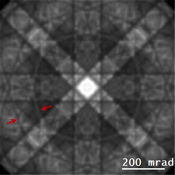
Figure 2a shows the [001]-Si EBSD pattern simulated with only phonon scattering, that is, plasmon scattering was not included. Five phonon configurations were averaged. Kikuchi bands, as well as excess and defect Kikuchi lines (arrowed), are visible. In Bloch wave simulations, due to the phenomenological treatment of phonon scattering, the atom scattering factor must be modified to reproduce the anisotropy of Kikuchi line intensities (Winkelmann, Reference Winkelmann2008). Multislice simulations, however, have no such limitation and, therefore, better reproduce the expected intensities. Figure 2b shows the simulated [001]-Si EBSD pattern with both phonon and plasmon scattering. A total of 50 plasmon/phonon configurations were simulated for each EBSD pixel. The Kikuchi lines are barely visible, and the contrast of the Kikuchi bands are also a lot weaker. The EBSD patterns for “zero” energy loss as well as one, two, three, four, and six plasmon events are shown in Figures 2c–2h, respectively (here, “zero” energy loss includes the phonon losses during backscattering as well as propagation to the specimen surface). The “energy-filtered” EBSD patterns were taken from the same simulation dataset in Figure 2b. The Kikuchi band contrast increases between “zero” energy loss (Fig. 2c) and one plasmon event (Fig. 2d), but decreases for higher-order plasmon scattering, such that by six plasmon events (Fig. 2h) even the Kikuchi bands are barely visible. This trend of maximum contrast at an energy loss greater than the recoil energy is consistent with experimental results on energy-filtered EBSD (Deal et al., Reference Deal, Hooghan and Eades2008; Vos & Winkelmann, Reference Vos and Winkelmann2019). It should be noted that in the simulation, only the number of plasmon events as the backscattered electron leaves the specimen is recorded, while in experiment what is measured is the absolute energy, which also includes any energy loss prior to the backscattering event. This means that the maximum contrast measured by experiment will be shifted to higher energy losses compared to simulation.

Fig. 2. (a) 5 kV [001]-silicon EBSD pattern simulated with only phonon scattering and no plasmon losses. The red arrows denote excess and defect Kikuchi lines. (b) 5 kV [001]-silicon EBSD pattern including plasmon losses. The “energy-filtered” EBSD patterns for “zero” loss, one, two, three, four, and six plasmon losses are shown in (c– to (h), respectively. The numerical value at the top right-hand corner is the percentage contribution of each diffraction pattern to the total intensity in (b). The dark corners in the diffraction patterns are due to bandwidth limiting in the multislice simulations.
Figure 3 shows the number of TDS backscattering events contributing to the EBSD pattern of a given energy plotted as a function of specimen depth. For visual clarity only results for “zero” loss, double plasmon and six plasmon events following backscattering are plotted. “Zero” loss backscatter events occur close to the beam entrance surface, but as the energy loss increases, the distribution broadens and shifts deeper into the solid. This is consistent with the trends expected of a Poisson distribution. Kikuchi band contrast is a result of phonon scattering, which is estimated to have a longer mean free path compared to elastic or plasmon scattering (Vos & Winkelmann, Reference Vos and Winkelmann2019). Since “zero” loss backscatter events are confined to the near-surface region, there is much less phonon scattering that occurs as the electrons escape the solid. Consequently, for good Kikuchi band contrast, the backscatter event must occur deeper within the material, a criterion that is satisfied at higher energy loss. However, there is a trade off since beyond a certain number of plasmon scattering events the contrast starts decreasing again due to the so-called plasmon “de-channeling” effect (Mendis, Reference Mendis2019). For strong phonon scattering, the electron beam must first channel along the atom columns. During plasmon excitation, the incident electron is deflected on average by θ E, which is relatively small for a single plasmon event (e.g., 1.7 mrad at 5 kV). For multiple plasmon scattering, however, the cumulative effect of the beam deflection is such that the channeling, and hence Kikuchi band contrast, is diminished.

Fig. 3. The number of TDS backscattering events of a given energy plotted as a function of specimen depth. The data are extracted from the 5 kV [001]-silicon EBSD simulations (Fig. 2) and includes results from 50 plasmon configurations. For clarity, only the results for “zero” loss, double, and six plasmon energy losses are shown.
The ratio (θ B/θ E), where θ B is the Bragg angle, can be taken as a simple measure of the strength of plasmon de-channeling. The larger θ E is compared to θ B, the stronger the de-channeling during plasmon excitation; recall that a variation in incidence angle by ~θ B is sufficient to change the channeling behavior of the incident electrons (Hirsch et al., Reference Hirsch, Howie, Nicholson, Pashley and Whelan1965). It is easy to show that (θ B/θ E) is proportional to √E, where E is the energy of the backscattered electron. Therefore, plasmon scattering should have a greater effect on Kikuchi band contrast at lower electron energies. In the simulations, we only considered energies close to the 5 keV primary beam energy, although the energy spectrum of backscattered electrons covers the full range of values (Deal et al., Reference Deal, Hooghan and Eades2008). This is due to energy loss of the incident electrons prior to the backscattering event, as well as the fact that backscatter electrons can escape from depths far larger than the 100 Å considered in the present simulations. Therefore, it is necessary to simulate all allowed electron energies and not just small energy losses (Callahan & De Graef, Reference Callahan and De Graef2013; Pascal et al., Reference Pascal, Singh, Callahan, Hourahine, Trager-Cowan and De Graef2018). However, those electrons with energy significantly less than the primary beam energy are likely to have been backscattered from deeper within the specimen. While escaping the solid the electrons will therefore, on average, undergo multiple plasmon scattering. Since the ratio (θ B/θ E) is also smaller for these electrons, they are likely to generate very little Kikuchi band contrast and therefore only contribute to the background signal. This is probably the reason why the relative intensity of the featureless background in experimental EBSD patterns increases with the primary beam energy, as demonstrated for a silicon [001] single crystal in Figure 4. Higher primary beam energies have a larger spread in backscattered energy values, and since Kikuchi band contrast is contained predominantly in those electrons with small energy losses, there will be more electrons in the “tail” of the energy distribution that contribute to the background signal. Finally, we note that EBSD is related to electron channeling patterns (ECP) through the principle of reciprocity (Joy et al., Reference Joy, Newbury and Davidson1982; Wells, Reference Wells1999), so that plasmon excitations should have a similar effect on the latter.

Fig. 4. Experimental EBSD patterns from a [001]-silicon single crystal acquired at (a) 5 kV, (b) 15 kV, and (c) 25 kV. Only the unprocessed EBSD patterns are displayed, that is, the background intensity has not been subtracted. Note that due to the 70° tilt of the specimen the [001] zone-axis appears at the top of the EBSD pattern, as indicated in (a).
ECCI Profile of a Screw Dislocation
Figure 5a shows the ECCI profile across the ½[110] screw dislocation obtained from a simulation that included phonon, but no plasmon, scattering. Ten phonon configurations were averaged. The ECCI profile shows a left-right asymmetric intensity, consistent with previous experimental and simulated results (Wilkinson & Hirsch, Reference Wilkinson and Hirsch1997; Zaefferer & Elhami, Reference Zaefferer and Elhami2014; Kriaa et al., Reference Kriaa, Guitton and Maloufi2019). The asymmetry is due to the dislocation strain field causing a reversal in lattice plane bending, and therefore electron beam channeling, either side of the dislocation. There is also a narrow (~30 Å width) peak in ECCI intensity at the dislocation core, which to our knowledge has not been reported previously, probably due to the resolution being better in the simulation compared to experiment and/or signal-to-noise issues arising from a large background in the experiment. Changing the sense of the dislocation displacement [equation (7)] reversed the left-right asymmetry of the ECCI intensity profile, but the small peak at the dislocation core remained.

Fig. 5. (a) ECCI intensity profile across a ½[110] screw dislocation in silicon at a depth of 50 Å from the free surface. The sample is tilted for strong g = ±220 systematic row excitation in the symmetry orientation. The screw dislocation is at the origin of the graph. The simulation includes only phonon scattering and no plasmon losses. (b) The same ECCI profile but with plasmon losses also included. (a, and (b) Plotted on the same intensity scale to aid direct visual comparison. The “energy-filtered” ECCI profiles for “zero”, one, two, three, four, five, and six plasmon losses are shown on the same intensity scale in (c– to (i), respectively. In all simulations, the 5 kV incident beam had a 10 mrad probe semi-convergence angle and zero electron-optic aberrations.
Figure 5b shows the ECCI profile after including plasmon losses; 100 phonon/plasmon configurations were averaged. Unlike EBSD patterns, there is no significant change compared to the pseudo-elastic result (Fig. 5a). The ECCI profiles for “zero” loss and one to six plasmon losses are shown in Figures 5c–5i, respectively (note that only plasmon events prior to backscattering are recorded). Interestingly, all the “energy-filtered” ECCI profiles look very different from Figure 5b, indicating that there is not one dominant contributing energy loss. This can be understood by comparing plasmon de-channeling with the change in channeling conditions induced by the dislocation strain field. The change in deviation parameter s d for a reciprocal vector g due to a displacement vector field u is given as follows (Hirsch et al., Reference Hirsch, Howie, Nicholson, Pashley and Whelan1965; Kriaa et al., Reference Kriaa, Guitton and Maloufi2019):
 $$s_{\rm d} = {\mathbf {\bf g}}\cdot \displaystyle{{\partial {\mathbf {\bf u}}} \over {\partial z}}.$$
For our simulations, the 220 reflection g is parallel to u. The magnitude of u is given by equation (7) and z represents the spatial coordinate along the electron optic axis. Similarly, the deviation parameter vector sg for an incident wavevector Ko in a perfect crystal satisfies (Spence & Zuo, Reference Spence and Zuo1992):
 $$2{\mathbf {\bf K}}_{\rm o}\cdot {\mathbf {\bf s}}_{\rm g} = K_{\rm o}^2 -\vert {{\mathbf {\bf K}}_{\rm o} + {\mathbf {\bf g}}} \vert ^2.$$
It follows that for normal incidence, the change in deviation parameter (s p) following plasmon scattering is approximately
 $$s_{\rm p} = {-}{\mathbf {\bf g}}\cdot \displaystyle{{\Delta {\mathbf {\bf k}}_{\rm t}} \over {K_{\rm o}}}.$$
Equation 10 is evaluated assuming g is parallel to Δkt and |Δkt| ≈ K oθ E (small-angle approximation). The ratio |s d/s p| is then a simple measure for evaluating the role of plasmon scattering on ECCI contrast. If the ratio is large plasmon de-channeling is relatively minor and the ECCI contrast will mainly be due to the dislocation strain field. Figure 6 maps the logarithm of the |s d/s p| ratio as a function of position in the (110) plane (see Fig. 1b), with the screw dislocation end-on and at the origin of the plot. Plasmon de-channeling is only significant in regions where |s p|>|s d|, that is, when the logarithm of |s d/s p| has a negative value. From Figure 6, this condition is satisfied in only small regions of the 100 Å thick simulation “volume”. Furthermore, close to the dislocation core region, the |s d/s p| ratio is several orders of magnitude large. For dislocations close to the beam entrance surface, the ECCI contrast will, therefore, be dominated by the intrinsic strain field. Plasmon losses have a negligible effect, as confirmed by the simulation results in Figure 5. Backscattered electrons with energy significantly lower than the primary beam energy are likely to be generated deeper within the sample, where the dislocation strain field is small. Therefore, these electrons do not produce any dislocation contrast and will only contribute a featureless background signal, similar to EBSD. Removal of this background, using for example a Timepix direct electron detector with energy thresholding [30], would improve the peak-to-background ratio of the ECCI signal and potentially enable analysis of the dislocation core structure (e.g., the small peak in Figs. 5a and 5b).

Fig. 6. Natural logarithm of the |s d/s p| ratio plotted as a function of position. The viewing direction is [110] with the dislocation end-on and at the origin. The dashed line represents the trace of the  $\lpar {1\bar{1}1} \rpar$ slip plane (see Fig. 1b).
Conclusions
The multislice method of Chen and Van Dyck has been extended to include plasmon losses and is used to simulate EBSD patterns and ECCI intensity profiles of a ½[110] screw dislocation in [001]-silicon. The EBSD simulations reproduce many of the trends observed experimentally. In particular, it is found that the Kikuchi band contrast is maximum for small energy loss (i.e., few plasmon scattering events) following backscattering. This can be understood by considering the competition between phonon scattering of the outgoing backscatter wave and plasmon de-channeling. For strong phonon scattering and Kikuchi band contrast, the backscatter event must take place deeper within the sample. However, this must be balanced by the fact that the probability for plasmon excitation is also greater; the cumulative effect of many plasmon events with characteristic scattering angle θ E is to de-channel the backscattered wave off the atom columns, thereby decreasing phonon scattering. For the same reason, it follows that those backscattered electrons with energy significantly lower than the primary beam energy will have very little Kikuchi band contrast and therefore contribute mainly to the background signal in an EBSD pattern. Simulated ECCI profiles for dislocations, on the other hand, show a very different behavior. Here, plasmon losses have a negligible effect on the ECCI profile because the lattice plane bending by the dislocation strain field has a greater effect on electron beam channeling, and hence backscattering, compared to the plasmon scattering angle θ E.
Acknowledgments
This research was partly supported under the Discovery Projects funding scheme of the Australian Research Council (Project No. FT190100619) and the North East Centre for Energy Materials funded by EPSRC, UK (Grant No. EP/R021503/1).
APPENDIX
In this section, we compare simulated elastic backscattered diffraction patterns with experimental EBSD patterns. The elastic backscattered wave can be calculated using the Chen & Van Dyck (Reference Chen and Van Dyck1997) multislice method. The solution has a simple form [see equation 48 in Chen & Van Dyck (Reference Chen and Van Dyck1997)] in the “single backscattering” approximation, where multiple backscattering events are assumed to be negligible. Note that since the backscattering is purely elastic (i.e., TDS scattering is only in the forward direction), the backscattered waves from different specimen depths can interfere with one another (Chen & Van Dyck, Reference Chen and Van Dyck1997). Fourier transforming the net wavefunction at the specimen surface gives the backscattered diffraction pattern.
Figure A.1a shows the simulated [001]-silicon elastic backscattered diffraction pattern for a 5 kV, aberration-free, 10 mrad semi-convergence angle probe at normal incidence. The specimen thickness was 100 Å and ten phonon configurations were averaged. Plasmons were not included in the simulations. The intensity of the Kikuchi bands are much weaker compared to the Bragg reflections (the intensity is plotted on a logarithmic scale). The diffraction pattern for the forward scattered wave at the specimen exit surface (Fig. A.1b), on the other hand, displays more prominent Kikuchi bands along with Bragg reflections. Experimental EBSD patterns (e.g., Fig. 4) are dominated by Kikuchi band contrast and only occasionally show weak RHEED (reflection high-energy electron diffraction) spots (Vespucci et al., Reference Vespucci, Winkelmann, Naresh-Kumar, Mingard, Maneuski, Edwards, Day, O'Shea and Trager-Cowan2015). This is inconsistent with Figure A.1a and indicates that high-angle TDS is the dominant contribution to EBSD patterns even in crystalline specimens.

Fig. A.1. (a) 5 kV elastic backscattered diffraction pattern from a 100 Å thick, [001]-silicon sample. The forward scattered diffraction pattern is shown in (b). The intensities are displayed on a logarithmic scale and the dark regions at the corners are due to bandwidth limiting in the multislice simulations.


 Open access