


Introduction
Polymeric substrates comprising local mechanical stiffness pattern or nanostructural features are intensively investigated in the context of applications such as haptic displays (touchpads), stretchable electronics, mechanical and optical data storage devices,[Reference Ouchi, Yang, Suo and Hayward1–Reference Chen, Jin, Suo and Hayward8] or as instructive cell substrates guiding mechano-sensitive (stem) cells.[Reference Discher, Janmey and Wang9–Reference Juhee, Sujin, Sukho and Junghoon15] While individual cells can react to structural features of few nanometers in size and mechanical differences in the Pascal (Pa) range,[Reference Discher, Janmey and Wang9, Reference Yang, Wang, Gu and Leong14] the tactile sensitivity of a human finger is only capable of detecting structural features above 10 nm and local mechanics in the kPa regime.[Reference Kuroki and Nishida16–Reference Abdouni, Djaghloul, Thieulin, Vargiolu, Pailler-Mattei and Zahouani20]
Mechanically patterned surfaces can be realized by variation of the polymer's chemical composition (e.g., phase separated blends)[Reference Raczkowska, Prauzner-Bechcicki, Dąbczyński and Szydlak2] or crosslinking density (e.g., hydrogels).[Reference Discher, Janmey and Wang9, Reference Kuo, Xian, Brenton, Franze and Sivaniah21] Another approach is based on placing rigid microstructures or defined closed cavities (pores)[Reference Hu, Zhou, Liu and Ng22] under soft/elastic polymeric materials and applying pressure.[Reference Pham, Xue, del Campo and Salierno11]
In most technical applications (i.e., touchpads or data storage) the programmability of the material's surface is a central requirement. Thermally-triggered shape-memory polymers (SMPs)[Reference Lendlein and Kelch23] are a class of smart polymers that allow the realization of programmable surface structures. Here, thermal transitions (e.g., melting T m or glass transition T g temperature) are utilized as molecular switches that fix/stabilize a deformed (temporary) shape during a heating–deformation–cooling procedure, called programming. The obtained temporary shape is long-term stable until the programmed materials are again exposed to temperatures above the switching temperature, which causes recovery of the original shape. Besides the shape-memory effects on macroscopic specimens, the topographical recovery of microstructures on the surfaces of SMP films has also been reported, where programming was realized by vertical or tilted compression of the substrates, or via stretching the specimen in an elastic mold.[Reference Eisenhaure, Xie, Varghese and Kim24–Reference Jiang, Mansfeld, Fang, Kratz and Lendlein28] Among the SMP materials, polymer networks with broad melting or glass transition temperatures are of particular interest, as these allow the adjustment of the switching temperature (the temperature of maximum recovery rate) by variation of the deformation temperature within the thermal transition.[Reference Bae, Choi and Suh7, Reference Jiang, Mansfeld, Fang, Kratz and Lendlein28–Reference Nochel, Reddy, Wang, Cui, Zizak, Behl, Kratz and Lendlein33]
In this study we explored whether flat polymeric substrates with a distinct mechanical pattern can be obtained by applying temperature-memory programming to microstructured polymer substrates. We hypothesize that to achieve a substrate that is flat at the nanometer scale, the application of a specific deformation temperature (sT prog) during programming is required, where the contractive effects during cooling under stress are compensated (see Scheme 1).
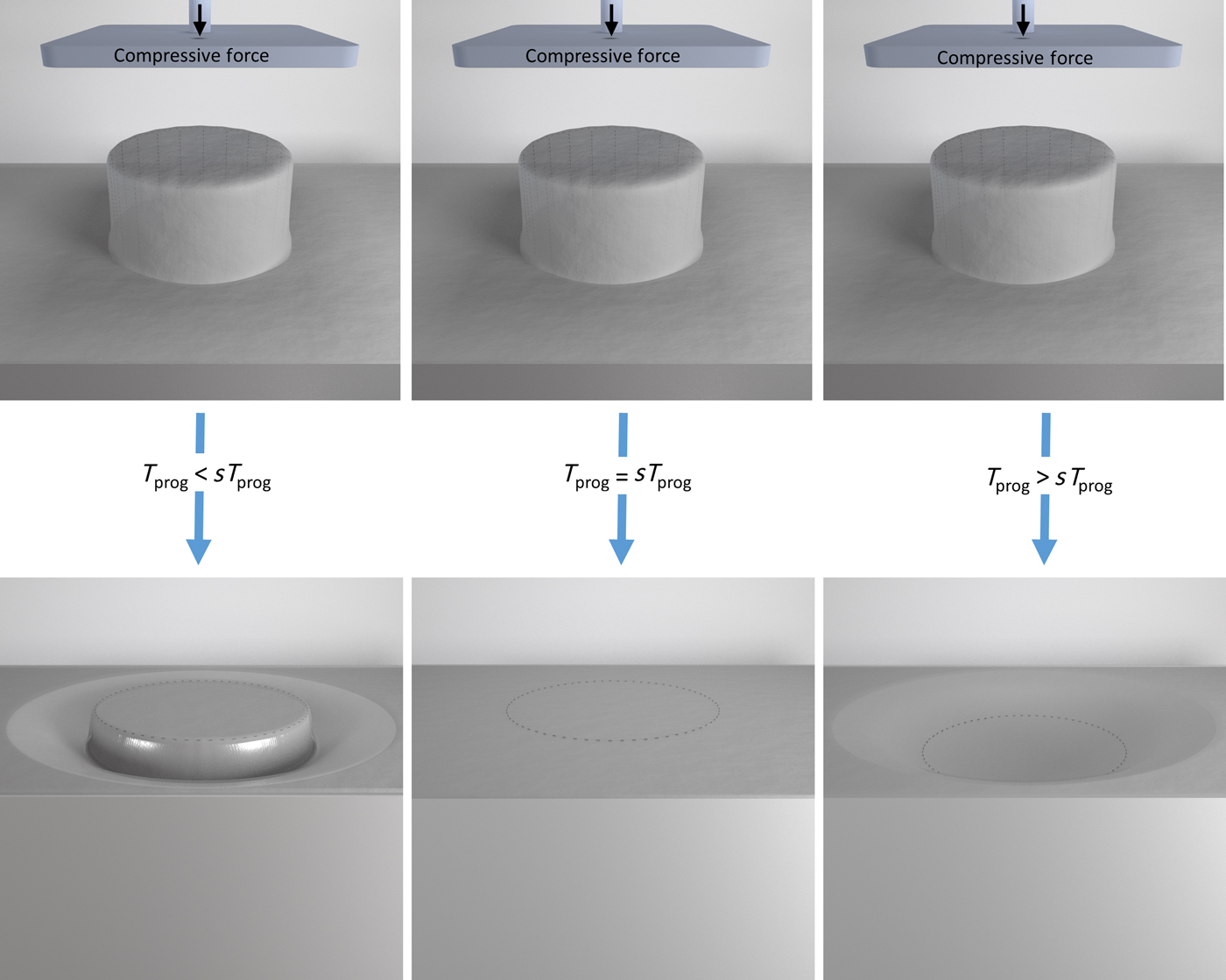
Scheme 1. Schematic representation of programming originally microstructured polymer substrates into flat substrates by application of a specific deformation temperature sT prog (center). At deformation temperatures below sT prog the incomplete impression results in remaining elevated features while deformation above sT prog generates small cavities caused by local, oriented crystallization during cooling under stress.
Our concept for achieving flat polymeric substrates with a defined (programmable) microscale stiffness pattern involves pressing elevated microstructures of a temperature-memory polymer into the underlying substrate without significantly compressing the whole polymer film. As polymer materials with crystallizable switching segments have advantages in terms of the stability of temporary shapes, we have chosen cross-linked poly(ethylene-co-vinyl acetate) (cPEVA) with a broad polyethylene melting transition for this work. For the substrates (thickness = 500 µm), a topographical design consisting of an array of microcylinders 50 µm apart, each with a diameter of 25 µm and a height of 10 µm was chosen. Here the volume of the microstructures represents 0.2% of the total substrate volume. The cPEVA substrates were prepared by an integrated process, whereby shaping and crosslinking occur simultaneously. Temperature-memory programming of the microstructured SMP surfaces to form flat substrates was realized by vertical or tilted compression at deformation (programming) temperatures from 60 to 100 °C and a fixation temperature of 10 °C, which were previously reported to result in an excellent shape fixation (R f ≥ 90%).[Reference Jiang, Fang, Kratz and Lendlein26, Reference Kratz, Madbouly, Wagermaier and Lendlein29, Reference Nochel, Reddy, Wang, Cui, Zizak, Behl, Kratz and Lendlein33, Reference Jiang, Mansfeld, Fang, Kratz and Lendlein34] The thermomechanical properties of the obtained microstructured substrates were explored by differential scanning calorimetry (DSC) and dynamic mechanical thermal analysis (DMTA). Original and programmed flat surfaces were analyzed by scanning electron microscopy (SEM), while the microcylinder height and local mechanical stiffness were examined by atomic force microscopy (AFM) and nanoindentation.
Experimental
Preparation of microstructured cPEVA substrates
Microstructured cPEVA substrates were prepared utilizing a fabrication scheme integrating shaping and covalent crosslinking according to the method described in the literature.[Reference Jiang, Fang, Kratz and Lendlein26, Reference Jiang, Mansfeld, Fang, Kratz and Lendlein28] In brief, in a first step a blend film composed of PEVA with vinyl acetate content of 18 wt% (trade name “Elvax460”, DuPont de Nemours, Neu-Isenburg, Germany) and the crosslinking agent dicumyl peroxide (Sigma-Aldrich Chemie GmbH, Taufkirchen, Germany) was solution casted from toluene (Sigma-Aldrich Chemie GmbH, Taufkirchen, Germany). In the next step microstructuring of the blend film was achieved by thermal embossing at 140 °C with a nanostructured poly(dimethylsiloxane) mold, having equidistant cylindrical microcavities with a depth of 10 µm and a diameter of 25 µm, and subsequently increasing the temperature to 220 °C for 30 min for cross-linking. The obtained microstructured cPEVA substrates had a thickness of around 500 µm.
Thermomechanical characterization
DSC experiments were conducted on a Netzsch DSC 204 Phoenix (NETZSCH Group, Selb, Germany) at heating and cooling rates of 10 K/min in sealed aluminum pans. A typical testing cycle is as follows. The polymer samples were first heated from room temperature to 150 °C to remove the processing related thermal history. The sample was then cooled from 150 to −100 °C and subsequently heated to 150 °C. Both temperature changes were analyzed with regard to the peak crystallization (T c) and melting temperature (T m).
DMTA measurement was carried out on an Eplexor 25N (Gabo, Ahlden, Germany) equipped with a 25 N load cell using the standard type test specimen (DIN EN ISO 527-2/1BB) in compression mode. The applied oscillation frequency was 10 Hz. The measurement was performed in the temperature sweep mode from −100 to 150 °C with a constant heating rate of 2 °C/min.
Temperature-memory programming of flat substrates
For temperature-memory programming, the microstructured substrates (area = 0.5 cm × 0.5 cm) were placed between two smooth silicon wafers and compressed (vertically or at an angle) at temperatures ranging from T prog = 60 to 100 °C for 20 min using foldback clips (width 25 mm) providing a force of approximately 20 N.[Reference Liu, Razzaq, Rudolph, Fang, Kratz and Lendlein35] Subsequently the whole sandwich was cooled to 10 °C and maintained at this temperature for 20 min prior pressure release.
Scanning electron microscopy
The original as well as programmed cPEVA substrates were analyzed at room temperature using an environmental scanning electron microscope (ESEM) (Quanta FEG 250 (FEI, Eindhoven, The Netherlands) operating at 30 kV equipped with a gaseous secondary electron detector. The samples were inspected with iridium coating.
Polarized optical microscopy
Polarized optical microscopy (POM) analysis was conducted using a Zeiss AxioImager A1m microscope, which was equipped with a Zeiss Axiocam MRC CCD camera and ZEN software (all Carl Zeiss Microscopy GmbH, Jena, Germany). The programmed samples were cut using a razor blade at ambient temperature into cross-sections with a thickness of around 50–70 µm and were placed on a glass coverslip. The orthoscopic images were recorded in transmission mode (and 0° position of the polarizer) with an objective Zeiss A-Plan 40×/0.65 Pol (Carl Zeiss Microscopy GmbH, Jena, Germany) at ambient temperature.
Characterization of original and programmed substrates by AFM
AFM measurements at ambient temperature were performed using a MFP-3D-Bio™ AFM (Asylum Research, Goleta, USA). Tapping mode (AC) with a scan rate of 0.5 Hz was applied to characterize the topographies of single microcylinders, as reported elsewhere.[Reference Jiang, Fang, Kratz and Lendlein26] A scan size of 50 µm × 50 µm was chosen for investigation of height and diameter of individual microcylinders. The apparent height, H, determined by AFM represents the height at the center of the microcylinders and relative to the level of the surrounding interspace surface of the substrate. Five individual microcylinders were analyzed for determination of H. Three-dimensional (3D) AFM images of the obtained raw data (height images and surface roughness) were processed using software MountainsMap® (Digital Surf, Besançon, France). The shape fixity ratio (R f) of the programmed single microcylinders was calculated according to Eq. (1):
 $$R_{{\rm f\;}} = \; \displaystyle{{H_0-H_{\rm \mu}} \over {H_0}} \times 100\% $$
with H 0 and H μ being the apparent heights of original and programmed (temporary) microcylinder, respectively.
Contact mode was applied to characterize the local reduced E-modulus of microstructured surface at the microscopic level. The probe type AC160TS (Olympus, Tokyo, Japan) with a typical driving frequency of 300 kHz (individual difference ranging from 200 to 400 kHz) and a typical spring constant of 26 N/m (individual difference ranging from 8.4 to 57 N/m) was used. Before indenting samples, the cantilever was first calibrated for the deflection inverse optical lever sensitivity (Defl InvOLS) by indentation on a clean smooth silicon wafer, and then calibrated for the spring constant by the thermal method using Asylum Research software (IGOR Pro, Wavemetrics, Inc.). In this mode, force maps with 20 × 20 indents with a size of 60 µm × 60 µm, containing a single micropillar at the center and surrounding inter-pillar space were obtained. Force was applied from 7.0 to 8.5 µN in order to keep the deformation depth at around 500–600 nm. The reduced E-modulus map was obtained by analyzing the force map using Asylum Research software. The Oliver-Pharr model[Reference Deuschle, Enders and Arzt36, Reference Oliver and Pharr37] was utilized to fit the single force curves and the reduced E-modulus was calculated by the fitting from 60% to 90% of indentation depth. The Poisson ratio (ν) of cPEVA was assumed to be 0.5, similar to that of rubber.[Reference Koblar, Škofic and Boltežar38] The average of 16 points at the center of single micropillar was taken as the reduced E-modulus of single microcylinder (E m), and the average of 25 points at each corner of the force map was taken as the reduced E-modulus of inter-pillar space (E i).
Results and discussion
Microstructured cPEVA substrates comprising microcylinders with a diameter of 25 µm, a height of 10 µm, and inter-pillar distance of 50 µm were fabricated via an integrated structuring process. Here the total volume of all microcylinders represents 0.2% of the overall substrate volume. The uniformity of the microcylinders was visualized by SEM, showing arrays of identical cylinders across the substrate area, while an average height of the cylinders of 10.0 ± 0.1 µm was determined by AFM (Fig. 1).
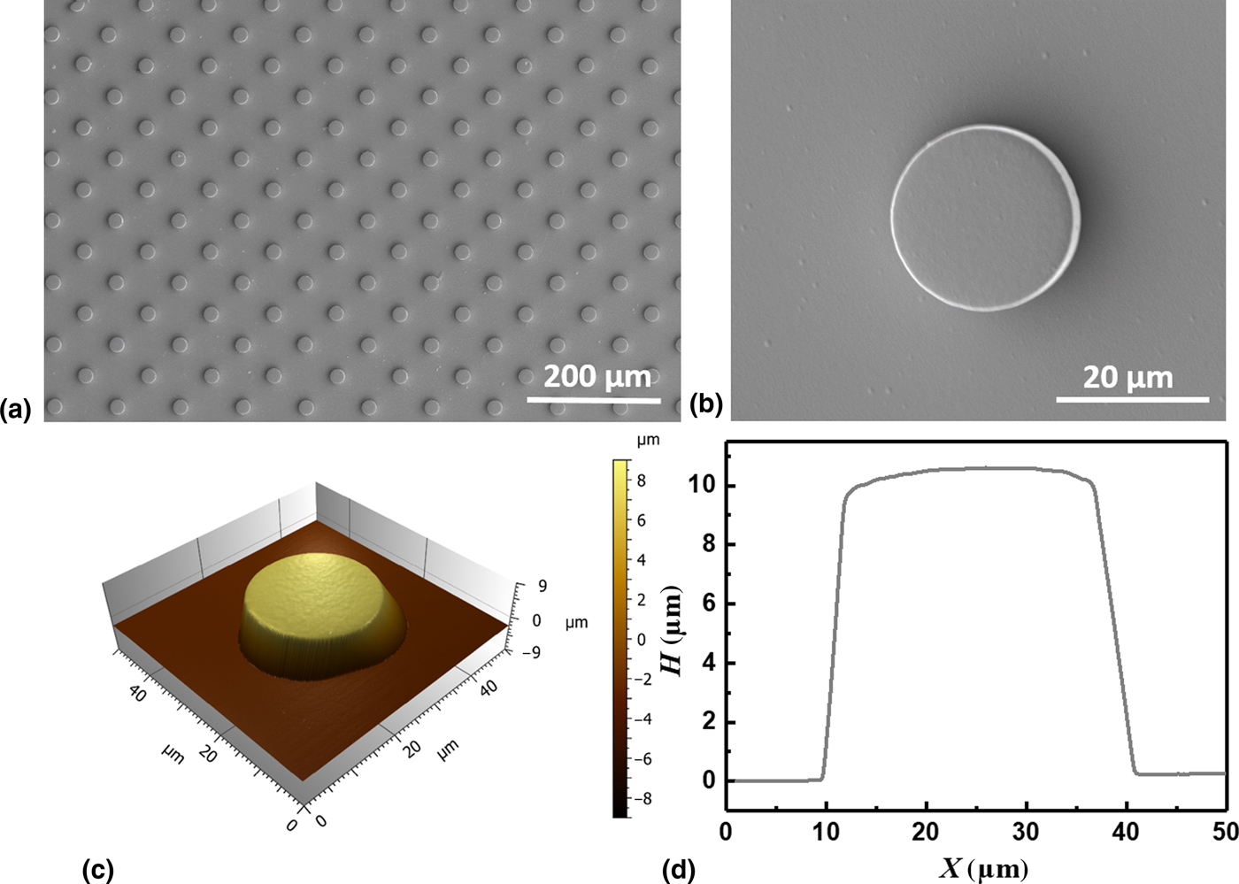
Figure 1. Surface characteristics of original microstructured cPEVA substrate. SEM image of the surface showing regular cylinder arrays (a) and a single microcylinder (b); 3D reconstruction of AFM scan of a single microcylinder (c) and the related height profile (d).
The thermomechanical characteristics of the original cPEVA substrates were examined by means of DSC and DMTA. DSC results revealed a broad melting transition of the cPEVA substrates in the range of 40–90 °C with a peak maximum at T m = 82 ± 1 °C during heating, while upon cooling a peak crystallization temperature of T c = 62 ± 1 °C was observed [Fig. 2(a)]. A pronounced maximum in the tan δ temperature curve was found at −15 °C in DMTA experiments, which can be attributed to the glass transition of cPEVA [Fig. 2(b)]. The loss modulus decreases with increasing temperature from approximately 2 GPa at –50 °C to approximately 10 MPa at 100 °C [Fig. 2(b)]. Based on these results, the temperature-memory programming temperatures (T prog) were chosen in the range of 60–100 °C for investigating the influence of the applied T prog on the resultant temporarily flat substrates. In this context, a fixation temperature of 10 °C was applied to ensure proper crystallization (see the Experimental section). With increasing the deformation temperature from 60 to 100 °C the degree of crystallinity of the cPEVA material decreases, and consequently the stiffness of the substrate as represented by the reduction in loss modulus from E′ = 35 ± 1 MPa at 60 °C to E′ = 8 ± 1 MPa at 100 °C [Fig. 2(c)]. As the compressive force applied by the foldback-clips was constant in all programming procedures, it is anticipated that the decreasing stiffness with increasing programming temperature results in microcylinders being more fully compressed into the substrate. According to the DMTA results this would be the case at temperatures above 81 °C. During cooling to 10 °C with keeping the compressive stress local oriented crystallization at the microcylinder site should occur, which can cause formation of nanocavities.
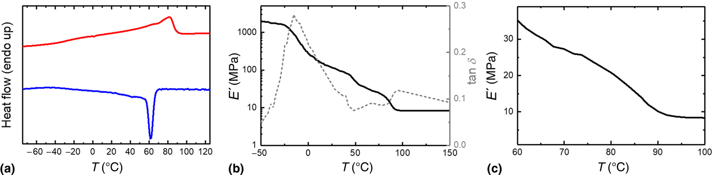
Figure 2. Thermomechanical characteristics of original microstructured cPEVA substrate. DSC heating and cooling thermograms (a), change in loss modulus (E ′) and tan δ with temperature obtained by DMTA (b), change in E ′ in the temperature range from 60 to 100 °C (c).
SEM investigation of the whole programmed sample revealed a more pronounced compression of the microcylinders into the substrate at the areas close to fixing foldback clips, when compared with the center of the sample. Therefore, all further SEM and AFM investigations were conducted with sample sections from the central area. Representative SEM images of the differently programmed substrates and single microcylinders confirmed a decrease in height of the compressed microfeatures with increasing T prog from 60 to 100 °C (Fig. 3). From these SEM micrographs it becomes further obvious that up to T prog = 72 °C the compressed microcylinders are surrounded by a ring-shaped trench. A similar phenomenon was observed for programmed cPEVA surfaces comprising arrays of pyramids, which were applied for dry adhesion purposes.[Reference Eisenhaure, Xie, Varghese and Kim24] The displayed SEM micrographs further indicated that width and depth of the trench decreases with variation of T prog from 60 to 72 °C.

Figure 3. SEM images of flat cPEVA substrates and single microcylinders vertically programmed at different temperatures of (a) 60 °C, (b) 70 °C, (c) 72 °C, (d) 75 °C, and (e) 80 °C.
The analysis of the programmed microcylinders by AFM revealed a decrease in microfeature height from 1.3 ± 0.1 to 0.4 ± 0.1 µm with increasing the programming temperature from 60 to 80 °C. The excellent fixation of the deformation was documented by high shape fixity ratios ranging from R f = 87 ± 1% to R f = 104 ± 1%. Here, R f-values above 100% might result from the contractive local oriented crystallization effects. It could be further observed that the depth and width of the surrounding trench vary when deformation was conducted at different temperatures. The obtained data are summarized in Table I and the 3D AFM images and height profiles are displayed in Fig. 4. While at deformation temperatures ≤70 °C elevated microstructures remained, an almost flat (compressed) microcylinder could be obtained when a specific deformation temperature of sT prog = 72 °C was applied to the selected substrate design. It can be assumed that the sT prog-value of structured polymeric substrates can be in addition influenced by the microstructures’ size and shape or the applied compressive force. Interestingly, the application of deformation temperatures ≥75 °C caused the formation of microcavities, which might be attributed to specific local contractive effects, induced by oriented crystallization during the programming process (i.e., compression and cooling under stress). It is assumed that the processes of deforming the microcylinder and impressing it into the underlying substrate generate local stress, which causes orientation of the macromolecules. As the local deformability increases with increasing programming temperature, different stress patterns should be obtained for cPEVA substrates programmed at different deformation temperatures. POM investigations were conducted to visualize the local stress in programmed cPEVA substrates (for details see the Experimental section). In Fig. 4(f) and (g), the POM images obtained for substrates programmed at T prog = 72 and 80 °C are shown. Here different stress concentrations became obvious, indicating a difference in the orientation of the macromolecules, which might be the cause of the formation of microcavities at T prog ≥ 75 °C during the oriented crystallization process. We anticipate that the mechanism of contraction is similar to that described for crystallizable water-blown polyurethane foams exhibiting reversible height and pore size changes upon repetitive heating and cooling after programming by compression.[Reference Zharinova, Heuchel, Weigel, Gerber, Kratz and Lendlein39] In contrast to the flat or elevated microfeatures, for such microcavities, no ring-shaped trench could be observed.

Figure 4. AFM 3D images and height profiles of cPEVA microcylinders vertically programmed at (a) 60 °C, (b) 70 °C, (c) 72 °C, (d) 80 °C, and (e) 100 °C. Polarized optical micrographs of substrates programmed at 72 °C (f) and 80 °C (g), the yellow arrows indicate the maximum stress concentration.
Table I Height (H), shape fixity ratio (R f), and relative reduced E-modulus (E m/E i) determined by AFM for cPEVA microcylinders which were vertically programmed at various T prog.

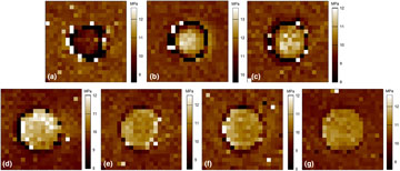
AFM nanoindentation was applied to characterize the local reduced E-modulus of the surface of the impressed microcylinders (E m) and the neighboring interface area (E i). The obtained reduced E-modulus maps for differently programmed cPEVA substrates are shown in Fig. 5. The stiffness difference between microcylinders and interspace was quantified by the relative ratio E m/E i. The original microstructured substrates exhibited a reduced E-modulus of E m = 9.6 ± 0.2 MPa, which was slightly lower than that of the surrounding interspace (E i = 10.1 ± 0.2 MPa). This difference might be related to the thermomechanical history implemented during the integrated structuring process or demolding. In contrast, for all programmed cPEVA substrates a higher reduced E-modulus (about 9–17%) was found at the surface of the impressed microcylinders, whereby lower deformation temperatures resulted in higher differences in stiffness. The highest difference between E m and E i (E m/E i = 117 ± 1%) was found for the substrates deformed at 70 °C. We attribute this observation to a higher degree of orientation of the macromolecules in the area of the microcylinders.

Figure 5. AFM reduced E-modulus maps of original cPEVA microcylinders (a) and the surrounding area and programmed by vertically compression at (b) 60 °C, (c) 70 °C, (d) 72 °C, (e) 75 °C, (f) 80 °C, or (g) 100 °C.
Conclusions
In this study we demonstrated that flat polymeric surfaces with a programmable stiffness pattern on microscale can be achieved by applying temperature-memory creation procedures to microstructured cPEVA substrates. Here the programming temperature was chosen as a key physical control parameter, which is capable of determining both the resultant surface topography and the local stiffness. All programmed samples showed a higher local stiffness on the microcylinder locations than on the interspace between the microstructures. It can be anticipated that the presented technology for achieving a programmable stiffness pattern on flat substrates is of relevance for haptic displays or cell instructive substrates.
Acknowledgments
This work was supported by the Helmholtz-Association through programme-oriented funding and by the German Federal Ministry for Education and Research through Grant No. 031A095. The authors thank Ms. Y. Pieper and Ms. D. Radzik for technical support and Dr. O.E. Gould for graphical support.


 Open access