


Introduction
With advancements in aberration correction, the spatial resolution of scanning transmission electron microscopy (STEM) has been enormously improved [Reference Haider, Rose, Uhlemann, Schwan, Kabius and Urban1, Reference Krivaneck, Nellist, Delby, Murfitt and Szilagyi2]. In addition to the reduction of the STEM probe size, a dramatic increase in the STEM probe current has been realized, leading to the routine acquisition of high-resolution elemental and chemical maps using electron energy loss spectrometry (EELS) [Reference Muller, Fitting Koukoutis, Murfitt, Song, Hwang, Silcox, Dellby and Krivanek3, Reference Lazar, Shao, Gunawan, Nechache, Pignolet and Botton4]. Using EELS combined with these advanced STEM instruments, atomic-level resolution information can be obtained from various types of materials, revealing the nature of interfaces, elemental distribution, presence of defects, and much more [Reference Wang, Saito, McKenna, Gu, Tsukimoto, Shluger and Ikuhara5, Reference Muller6]. In addition to simple elemental composition distributions, EELS is capable of delivering information about the chemical bonding, local atomic coordination, oxidation states, band gaps, and chemical phases of a broad range of materials at the fundamental resolution limit of the property being probed. Atomic-level EELS maps of these fundamental material properties can now be obtained with the acquisition time, to a large extent, limited only by the speed of the EELS spectrometer and not by the signal being measured. The availability of fast EELS spectrometers with large angular collection efficiencies [Reference Gubbens, Barfels, Trevor, Twesten, Thomas, Menon, Kraus, Mao and McGinn7] has closed the gap between the rate of signal generation in the specimen and the speed at which this signal can be detected. This significantly increases the amount of information that can be acquired using EELS. Using the most recent generation of spectrometers, EELS data can be acquired at well over 1,000 spectra per second with a high-duty cycle. Fifth-order spectral aberration correction in this generation of spectrometers allows the use of the large collection angles needed to match the increased convergence angle that Cs-probe-corrected systems present, improving collection efficiency while maintaining energy resolution. These advances, when taken together, result in a well matched source/detector system capable of recording high-energy EELS edges at atomic resolution at a rate fast enough to limit electron beam damage to the sample.
Methods and Materials
To illustrate these advances, data were acquired at Arizona State University using a probe-corrected JEOL ARM 200 STEM equipped with a Schottky FEG source operating at 200 kV. The EELS data were collected using a Gatan Enfinium® ER spectrometer that included: (a) DualEELS™ capability, which allows two different energy regions of the EELS signal to be recorded nearly simultaneously under the same experimental conditions [Reference Gubbens, Barfels, Trevor, Twesten, Thomas, Menon, Kraus, Mao and McGinn7, Reference Scott, Thomas, Mackenzie, McFadzean, Craven and Nicholson8]; (b) a 2-K CCD camera with a low dispersion mode, which allows the recording of EELS data with an energy range up to 2000 eV (4000 eV with DualEELS™); (c) fast acquisition mode, which allows acquisition of over 1000 spectra per second; (d) dodecapole lens system capable of correcting spectral aberrations up to the 5th order, which allows collection angles well over 100 mrad at 200 kV to be used with sub-eV energy resolution.
Two different samples were analyzed: a conventional SrTiO3 (STO) single crystal and SrTiO3/LaMnO3 (STO/LMO) interface. Both samples were prepared using standard cross-sectioning technique, which includes ion-milling as final stage using a Gatan PIPS. For the STO sample, EELS data were acquired using a 0.13 nm STEM probe containing a current of 115 pA. The probe convergence angle was 25 mrad and the EELS collection angle was estimated to be greater than 110 mrad. The EELS spectrum image acquisition (SI) was carried out in DualEELS™; the regions of the EELS spectrum from 350 eV to 2350 eV and 1000 eV to 3000 eV were simultaneously acquired in rapid succession using acquisition times of 4 ms and 11 ms, respectively. The total acquisition time was less than 16 ms with better than 94% live time for each of the 50 × 40 pixels of the spectrum image, and the entire EELS SI was acquired in one pass without any spatial drift correction. The sample experienced a minimal amount of spatial drift, as shown in the simultaneously acquired ADF image in Figure 1. At the short camera length used in this experiment, detectors fitted to the TEM column are at too high of an angle and detect only a weak STEM signal. An ADF STEM detector is fitted to the spectrometer, which is optimized to match the 5 mm collection aperture of the spectrometer, resulting in efficient collection of both the EELS and ADF signal at the short camera length required for this experiment.

Figure 1: ADF image of SrTiO3 acquired simultaneously during the EELS spectrum image acquisition demonstrating the high stability of the system.
For the STO/LMO interface specimen, the EELS SI was recorded using the same instrumentation described above, using a 0.15 nm STEM probe containing approximately 200 pA at a convergence angle of 25 mrad and directed into the spectrometer with a collection angle greater than 110 mrad. As above, the EELS SI data was taken in DualEELS™ mode, and the regions of the EELS spectrum from 280 eV to 2280 eV and 900 eV to 2900 eV were acquired in rapid succession using acquisition times of 4 ms and 14 ms, respectively. The total acquisition time per pixel for the 208 × 82 spectrum image in this case was less than 20 ms with better than 94% live time. The EELS SI was acquired without any spatial drift correction, and no spatial drift was observed.
Results
Mapping High-Energy Edges
Most work on atomic-level EELS mapping of SrTiO3 has been carried out using the Sr M4,5-edges at 130 eV and the Ti L2,3-edges at 456 eV. While low-energy M-edges, such as the Sr M4,5-edges, have large cross sections for energy loss events, the delayed nature of the M edge results in poor signal-to-background ratios. However, the higher signals available at the low-energy-loss end of the EELS spectrum show a higher signal-to-noise ratio for the same amount of current. Thus, as reported in [Reference Botton, Lazar and Dwyer9], the contrast in the Sr M4,5-edges map increases progressively as the integration window is shifted away from the actual edge threshold. The best contrast was achieved by placing the integration window from 360 to 410 eV beyond the Sr M4,5-edges onset. The contrast is improved from an increase in the edge cross section and a reduction in the background signal, giving an overall increase in the signal-to-background and signal-to-noise ratios. However, the delayed window placement may lead to misinterpretations because of carbon contamination with its K-edge at 284 eV and other possible element edges in that region of the EELS spectrum. This problem can be overcome by recording the Sr L2,3-edges at 1940 eV, but the absolute signal is significantly reduced compared to the Sr M4,5-edges at 130 eV. However, the signal-to-background ratio is dramatically improved, and the background is a nearly constant power law at these energies, leading to a more reliable background removal.
Simultaneous mapping of high-energy edges, such as the Sr L2,3 and lower ones such as the Ti L2,3 at 456 eV, is now be possible using the DualEELS™ [Reference Gubbens, Barfels, Trevor, Twesten, Thomas, Menon, Kraus, Mao and McGinn7, Reference Scott, Thomas, Mackenzie, McFadzean, Craven and Nicholson8] capability available in the GIF Quantum® and the Enfinium™ spectrometers. The acquisition time for both regions can be adjusted in such a way that the signal-to-noise ratio is maximized, and any saturation of the camera, which may occur during the acquisition of the intense low-energy region of the EELS spectrum, is prevented. Because of the increased probe current available in a probe-corrected STEM microscope, high-energy edges, such as the Sr L2,3-edges at 1940 eV, can be acquired with an acquisition time as short as 11 ms while maintaining a good signal-to-noise ratio. In this manner, it is possible to increase the dynamic range of the final EELS spectrum up to 4000 eV. In DualEELS™ every edge can be collected and the acquisition time adjusted accordingly. Figure 2 shows the EELS spectrum extracted after splicing the DualEELS™ data into a single continuous dataset.

Figure 2: Extracted SrTiO3 EELS spectrum after splicing the lower core-loss region at 350 eV and the higher core-loss region at 1000 eV of the DualEELS™ spectrum image. Both the Ti L2,3-edges and the Sr Ti L2,3-edges are present in the same spectrum. The dynamic range of the EELS spectrum is increased as a result of the splicing of the two datasets. Figures 2b and 2c are the enlarged regions of the EELS spectrum for the Ti L2,3-edges at 456 eV and the Sr Ti L2,3-edges at 1940 eV, respectively.
Background removal
Another problem that can be encountered when analyzing atomic-level EELS maps is background removal. In general, the background for core-loss edges is removed using power law fitting [Reference Egerton10], which is available in Digital Micrograph. Here the intensity of the background I is given by: I = Ae -r where E is the energy loss, and A and r are fitting constants that depend on the details of the experiment. At high-energy losses (above 900 eV), r is relatively constant, taking on a value between 2 and 3, whereas at low energies r may change with energy loss making the extrapolation problematic. Removing the background using the power law method can lead to errors in maps directly related to extrapolation errors in the fitting. However as reported in [Reference Riegler and Kothleitner11, Reference Leapman and Swyt12, Reference Door and Gangler13, Reference Thomas14], the background removal can be significantly improved using the multiple linear least square (MLLS) fitting approach for the background and the edge signal. Here the reference spectra needed for the fitting are the estimated background and edge after background removal. In this way, the background is forced to retain a constant shape across the whole region. The signal-to-noise ratio of the background-subtracted elemental maps is significantly improved, as shown in Figures 3 and 4. Such improvement can be also observed in Figures 5a and 5b, which show line profiles extracted from the same regions in the Ti and Sr elemental maps with the background removed using conventional power law method and the MLLS fitting procedure. The line profiles were extracted from regions between the atomic columns to show how the background modulates. All the line profiles are normalized. The background seems to fluctuate much less in the case of the MLLS fitting approach. The improvement is more evident in the case of the Ti L2,3-edges elemental map (Figure 3) where the background fitting is more problematic. As mentioned previously, the background fitting at high-energy edges is more robust and not significantly improved by standard MLLS fitting.

Figure 3: a) Extracted Ti L2,3-edges elemental map by simple background removal using a power law background and integrating over an energy window across the edge; b) elemental map extracted using the MLLS fitting procedure.

Figure 4: a) Extracted Sr L2,3-edges at 1940 eV elemental map by simple background removal using a power law background and integrating over an energy window across the edge from the threshold; b) elemental map extracted using the MLLS fitting procedure.

Figure 5: a) Extracted line profiles between two atomic columns from the same region in Figures 3a and 3b; b) Extracted line profiles between two atomic columns from the same region in Figures 4a and 4b. The MLLS fitting line corresponds to the elemental map where the background was extracted using the MLLS fitting approach, whereas the power law corresponds to the elemental map where the background was removed with the conventional power law method.
Figure 6 shows a colorized EELS elemental map of the Sr L2,3-edges at 1940 eV and the Ti L2,3-edges at 456 eV. The contrast between the Sr and Ti atomic columns is high, and this confirms the advantage of mapping high-energy edges when the system is capable of delivering high current. In addition to elemental contrast shown in these elemental maps, the L2,3-edges of Sr and Ti carry significant bonding information because of the strong coupling to the local density of states of the d-band electrons. Using MLLS fitting of the near edge fine structure, improved information can be obtained on the chemical state of the element under the beam [Reference Tan, Turner, Yucelen, Verbeeck and Van Tendeloo15, Reference Turner, Lazar, Freitag, Egoavil, Verbeeck, Put, Strauven and Van Tendeloo16].
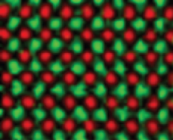
Figure 6: Elemental map of Sr L2,3-edge at 1940 eV (green) and Ti L2,3-edges at 456 eV (red) acquired in DualEELS™ mode.
Revealing the interface
The same approach was used to characterize the SrTiO3/LaMnO3 crystalline sample. The STO/LMO interface does not seem very visible in the high-resolution HAADF STEM images shown in Figure 7. The red rectangular box shows where the interface is located in the sample. However, EELS can give further insight into the chemistry and elemental distribution across the interface. Figure 8 shows colorized elemental maps obtained from the La M4,5-edes at 832 eV in yellow, the Mn L2,3-edges at 640 eV in blue, the Ti L2,3-edges at 456 eV in red, and the Sr L2,3-edges at 1940 eV in green. Note that there appears to be intermixing between Ti and Mn that extends for a couple of monolayers across the interface. This is evidenced in the colorized map by the presence of atomic columns showing both red and blue colors, which can be explained by the presence of both Ti and Mn in the same atomic columns. Quantitative analysis carried out across the same region shows the presence of 12% Ti and 10% Mn.

Figure 7: High-resolution ADF STEM image of SrTiO3/LaMnO3. The green box represents the area where the beam was scanned during the acquisition of the EELS SI. The red rectangular area shows where the interface is located.

Figure 8: Colorized map where the Sr L2,3-edges at 1940 eV is in green; the Ti L2,3-edges at 456 eV is in red; the La M4,5-edges at 832 eV is in yellow; and the Mn L2,3-edges at 640 eV is in blue.
Discussion
High- and low-energy edges in the EELS spectrum can be simultaneously acquired using the DualEELS™ capability available in the GIF Quantum® and Enfinium™ EELS spectrometers. In addition, the energy range of the acquired EELS data is effectively doubled and can extend up to 4000 eV. More importantly, by combining the increased probe current present in an aberration-corrected microscope with the fast EELS spectra acquisition capability available in the GIF Quantum® and Enfinium™ spectrometers, mapping high-energy edges at the atomic level with a good signal-to-noise ratio and in a short amount of time is now possible. The quality of such elemental maps in terms of contrast is shown in the Ti and Sr elemental maps (Figure 6). This is due to the high signal-to-background ratio that these edges show. Figure 9 shows EELS colorized elemental maps of Ti and Sr obtained in single-range EELS mode using the Sr M4,5-edges at 130 eV compared with the maps taken in DualEELS™ mode using the Sr L2,3-edges at 1940 eV. Both maps show quite similar contrast. However, it is important to mention that the maps acquired in single-range mode using the Sr M4,5-edges at 130 eV in Figure 9a are obtained with an integration window between 320 eV and 420 eV well beyond the Sr M4,5-edges onset at 130 eV. Therefore, these maps just show simple fluctuations of the background and are not reliable for quantification purposes. On the other hand, the elemental maps acquired in DualEELS™ mode in Figure 9b using the Sr L2,3-edges at 1940 eV are obtained by placing the integration window across the Sr L2,3-edges and can be used for quantification. Although the Sr L2,3-edges show a lower signal-to-noise ratio compared to the Sr M4,5-edges, the maps acquired in DualEELS™ mode show high contrast, perhaps higher than the ones taken in single-range mode using the Sr M4,5-edges at 130 eV. The high contrast shown by the maps acquired in DualEELS™ mode is due to the higher signal-to-background ratio.

Figure 9: a) Elemental maps of Sr (green) and Ti (red) in single-range EELS mode. The experiment was carried out at Florida State University with a 200 kV probe-corrected ARM TEM equipped with a cold FEG emission gun and a GIF Quantum EELS spectrometer. The 100-eV Sr M-edge integration window was taken from 320 eV to 420 eV, well beyond the Sr M4,5-edges at 130 eV. b) Elemental maps of Sr L2,3-edge at 1940 eV (green) and Ti L2,3-edges at 456 eV (red) from Figure 6.
Conclusion
We have shown that atomic EELS mapping is very effective using high-energy edges. The signal-to-background ratio is much higher, leading to a more reliable edge extraction. In addition, the background removal can be greatly improved using the MLLS fitting procedure. High- and low-energy edges in the EELS spectrum can be simultaneously acquired using the DualEELS™ capability available in the GIF Quantum® and Enfinium™ EELS spectrometers. In addition, the energy range of the acquired EELS data extended up to 4000 eV. More importantly, by combining the increased probe current present in an aberration-corrected microscope with the fast EELS spectra acquisition capability available in the GIF Quantum® and Enfinium™ spectrometers, mapping high-energy edges at the atomic level with a good signal-to-noise ratio and in a short amount time is now possible. The quality of such elemental maps in terms of contrast is high, as shown in the elemental maps showing Ti and Sr in one example and Sr, Ti, La, and Mn in a second experiment. This is due to the high signal-to-background ratio that these edges show. In addition, when the low-loss region is acquired along with the core loss, it is now possible to correct for plural scattering, compute specimen thickness, and perform absolute quantification in a routine fashion. In addition, the energy range of the acquired EELS data is effectively doubled and can extend up to 4000 eV. These are some of the many advantages of acquiring data using the DualEELS™ capability.
Acknowledgments
Particular acknowledgements go to Dr. Toshiro Aoki from JEOL USA who helped set up the microscope for both experiments, Professor Ray Carpenter at Arizona State University for letting us use his facilities, Professor David J. Smith at ASU for kindly providing the STO/LMO sample used in the second experiment, and Dr. Yan Xin at Florida State University for letting us use the facilities where we acquired the STO elemental map using low-energy edges.


