To save content items to your account,
please confirm that you agree to abide by our usage policies.
If this is the first time you use this feature, you will be asked to authorise Cambridge Core to connect with your account.
Find out more about saving content to .
To save content items to your Kindle, first ensure no-reply@cambridge.org
is added to your Approved Personal Document E-mail List under your Personal Document Settings
on the Manage Your Content and Devices page of your Amazon account. Then enter the ‘name’ part
of your Kindle email address below.
Find out more about saving to your Kindle.
Note you can select to save to either the @free.kindle.com or @kindle.com variations.
‘@free.kindle.com’ emails are free but can only be saved to your device when it is connected to wi-fi.
‘@kindle.com’ emails can be delivered even when you are not connected to wi-fi, but note that service fees apply.
Recently, the concept of creating a boron doped nanocrystalline diamond (B-NCD) based temperature regulator for bio-sensing applications was proven. In this work, the next step is taken, i.e. one device working simultaneously as thermistor and heater. In combination with a PID-control., it is possible to create a temperature control, with possible set points going from room temperature till 70°C, with an accuracy exceeding a maximum temperature variation of 0.2 °C. Parallel with steering the temperature by varying the current through the B-NCD film, its resistance is measured with a 4-point measurement from which the temperature can be derived using a calibration curve. This value is the feedback for the PID-control to steer the current used for the regulation.
Well-aligned, 1D CdSe quantum dot (QD) fibers (0.3μm to 2.5μm) containing up to 20wt% fluorescent quantum dots (QDs) were prepared by near-field electrospinning (NFES) process. Electrospun solutions were prepared using PVAc as the matrix polymer, dimethyl formamide (DMF) solvent and colloidal QDs in chloroform (CHCl3). The diameter of the fibers decreased as the ratio of DMF/CHCl3 is varied. QDs showed good dispersion and a linear relationship between QD loading and fiber diameter, as determined by the morphology measurements taken using TEM and SEM, respectively. Fluorescence microscopy shows that there is light attenuation throughout the fibers. Results also show that the NFES process may be used as a method to create aligned, 1D fibers of QDs and potentially other nanofibers.
Boron doped CVD diamond has been extensively studied in bulk form but little has been published regarding the effects that the initial seeding and growth conditions can have on the characteristics of the initial layer of diamond. This can have a dramatic effect on the performance of the film in applications ranging from AFM probe tips to electrodes used for water purification and other applications. This paper will examine how initial growth conditions and seeding methods can affect the film interface characteristics of doped diamond grown in hot filament CVD reactors.
The effects of substitute side chain were investigated using donor-acceptor (D-A) conjugated copolymers consisting of a cyclopentadithiophene (CPDT) derivative and dithienyl-benzothiadiazole (DTBT). The intrinsic properties of the copolymers were significantly altered by perturbations of the intramolecular charge transfer (ICT). The absorption of PCPDT-ttOTBTOT (P2), which assumed a tail-tail configuration, tended to blue-shift relative to the absorption of PCPDT-TBTT (P1). The absorption of PCPDT-hhOTBTOT (P3), which assumed a head-head configuration, was blue-shifted relative to that of P2. The electrical transport properties of field-effect transistors (FETs) were sensitive to the side chain position. The field-effect mobility in P2 (μ2=1.8×10⁻³ cm2/V·s) was slightly lower that in P1 (μ1=4.9×10⁻³ cm2/V·s). The mobility of P3, however, was very low (μ3=3.8×10⁻⁶ cm2/V·s). Photoexcitation spectroscopy showed that the charge generation efficiency (shown in transient absorption spectra) and polaron pair mobility in P1 and P2 were higher than in P3, yielding P1 and P2 device performances that were better than the performance of devices based on P3.
Small size CdS QDs were synthesized by (i) the single source precursormethodology and by (ii) the microwave synthetic route. The consequences ofCdS QD direct exposure to air for a period of 7 days were investigated byfollowing the evolution of the photoluminescence (PL) and absortion spectra.For QDs obtained by (i), the excitonic emission band (3.0 ‑ 3.1 eV)decreases in intensity, relatively to the low energy one (2.2 ‑ 2.5 eV)tentatively associated to midgap surface states. This suggests arising ofnew recombination path(s) associated to degradations during aging, possiblyan oxidative formation of a CdO surface layer. On the other hand, nosignificant change is observed in the absorption spectra. For QDs obtainedby (ii), no degradation is revealed by the PL spectra which remainunchanged. On the other hand, the absorption spectra are dominated by anunexplained broad band around 3.6 eV which tends to hide the fundamentalexcitonic transition one and increases in intensity with aging.
SiC nanowires were produced from carbon nanotubes and nanosize silicon powder in a tube furnace at temperatures between 1100°C and 1350°C. SiC nanowires had average diameter of 30 nm and very narrow size distribution. The surface of the SiC nanowires is covered by an amorphous layer composed of amorphous SiC and various carbon and silicon compounds. The objective of the research was to modify the surface structure of the SiC nanowires, a step necessary for future surface functionalization. The acid etched nanowires were analyzed using FTIR, TEM, x-ray diffraction, and photoluminescence. The concentration of Si-Ox groups in untreated specimens was estimated to account for 1% of the total mass of a 2 nm thick amorphous layer wrapping around all structures. After treatment in HF this concentration was negligibly small. TEM images show that after treatment the amorphous layer was removed but the diameter of the core remained unchanged. The surface was roughened and multiple pits formed on that surface. X-ray line broadening analysis indicates a significant contribution due to stress caused by dislocations and planar faults. After acid etching line narrowing was observed and attributed to stress reduction and elimination of the smallest wires. The photoluminescence signal from as received samples was very weak but increased greatly after acid treatment, indicating that the signal is related to surface defects. Measurements at low temperatures, 8 K, showed peaks due to point and planar defects.
Monolayers of cobalt phthalocyanine (CoPc) and fluorinated cobalt phthalocyanine (F16CoPc) on silver (111) and on highly (0001) oriented pyrolytic graphite (HOPG) were imaged with a scanning tunneling microscope (STM) at cryogenic temperatures (around 30 K) at Chemnitz University of Technology. Domains of regular arrays with periodicity in two dimensions (2D) and a variety of plane symmetries were observed. Crystallographic image processing (CIP) was used to quantify deviations from the plane symmetry groups and to obtain symmetrized versions of the content of the average unit cells of some of these arrays. Conclusions on the point symmetry of the CoPc and F16CoPc molecules within the arrays were drawn.
Polyaniline nanofibres (PAni) can be surface modified to improve electroactivity over a broader pH range. The technique we describe here can be used to attach carboxylic acid terminated substituents. Modified nanofibres maintain their high surface area, and ability to switch between different redox states. These properties make the material suitable for sensing applications. Unlike unmodified PAni, the functionalised material is self-doping and hence more stable in higher pH solutions. Here we demonstrate how modified PAni fibres can be used for the detection of ascorbic acid.
Vapor-liquid-solid (VLS) method has become one of the few and most powerful bottom-up single crystal nanowire growth techniques in nanotechnology due to its easy scalability from micro to nano feature sizes, high throughput, relatively low cost, and its applicability to various semiconductor materials. On the other hand, control of growth direction and crystal orientation of nanowires, which determine their electrical, optical, and mechanical properties, stand as major issues in VLS technique. In this study, we demonstrate a new vapor-liquid-solid glancing angle deposition (VLS-GLAD) fabrication approach to produce crystalline semiconductor nanowires with controlled geometry. VLS-GLAD is a physical vapor deposition nanowire fabrication approach based on selective deposition of nanowire source atoms onto metal catalyst nanoislands placed on a crystal wafer. In this technique, collimated obliquely incident flux of source atoms selectively deposit on catalyst islands by using “shadowing effect”. Geometrical showing effect combined with conventional VLS growth mechanism leads to the growth of tilted crystalline semiconductor nanowire arrays. In this study, we report morphological and structural properties of tilted single crystal germanium nanowire arrays fabricated by utilizing a conventional thermal evaporation system. In addition to the tilted geometry, by introducing substrate rotation, nanowires with various morphologies including helical, zig-zag, or vertical shapes can be fabricated. Engineering crystalline nanowire morphology by using VLS-GLAD have the potential of enabling control of optical, electrical, and mechanical properties of these nanostructures leading to the development of novel 3D nano-devices.
The effect of seawater on thermal behavior of conventional and nanophased carbon/epoxy composites was investigated in this study. Composites were fabricated with 1 wt.%, 2 wt.%, and 3 wt.% nanoclay by vacuum assisted resin transfer molding (VARTM) process and compared with neat samples with and without exposure to seawater. Thermal characterization was performed by the dynamic mechanical analysis (DMA) and thermogravimetric analysis (TGA). Samples exposed to the seawater for 30- and 60-day periods revealed that samples with nanoclay retained better thermal properties compared to the neat samples. Storage modulus was reduced by 6.28%, 6.76%, 6.15%, and 7.05% for neat, 1 wt.%, 2 wt.%, and 3 wt.% nanoclay infused samples, respectively, after the samples were exposed to seawater for 60 days . From TGA results, it was observed that the thermal stability is not related to nanoclay content and conditoning. Optical microscope (OM) and scanning electron microscope (SEM) studies revealed no significant change in surface morphology in the 30-day conditioning samples.
The effects of Ge and Ti additions on the microstructure, hardness and oxidation behaviour of the alloys Nb–18Si–5Ge (ZF1) and Nb–24Ti–18Si–5Ge (ZF3) were studied. The as cast microstructure of the alloy ZF1 consisted of Nbss (cI2), and βNb5Si3 (tI32) with the latter being the primary phase and the two phases forming high volume fractions of Nbss + βNb5Si3 eutectic. The Ge addition stabilised the βNb5Si3 (tI32), and destabilised the Nb3Si (tP32) and the Nbss + Nb3Si eutectic. After heat treatment at 1200 °C for 100 h the βNb5Si3 (tI32) was partially transformed to the αNb5Si3 (tI32), and equilibrium was reached after heat treatment at 1500 °C for 100 h. The phases present in the as cast alloy ZF3 were the Nbss (cI2), and the Nb3Si (tP32), βNb5Si3 (tI32) and Ti5Si3 (hP16) silicides, with the latter forming a eutectic with the solid solution. The same phases were present after heat treatment at 1200 °C for 100 h but only the Nbss, and the Nb3Si and Nb5Si3 silicides were present after 100 h at 1500 °C where TiO2 was also formed. The Ge addition increased the microhardness of the Nb5Si3. The synergy of Ti with Ge resulted in a strong hardening effect and a remarkable retention of the hardness of the alloy ZF3. The additions of Ge and Ti to the Nb-18Si alloy improved the oxidation resistance at 800 °C, but pest oxidation behaviour was not eliminated.
A polypyrrole (PPy) nanocellulose composite was shown to cycle well over 3000 cycles in 2.0 M NaCl electrolyte when used as the active material for both electrodes in an energy storage device. SEM micrographs show a highly porous nature of the conductive paper material and electrochemical charge-discharge measurements, as well as external electrode potential monitoring, confirm the good cycling behavior of the material.
We have measured electron drift in amorphous silicon-germanium nip photodiodes using the photocarrier time-of-flight technique. The samples show electron deep-trapping shortly after photogeneration, which is generally attributed to capture by a neutral dangling bond (D0) to form a negatively charged center (D-). An unusual feature is that electron re-emission from the trap is also clearly seen in the transients. Temperature-dependent measurements on the emission yield an activation energy of about 0.8 eV and the remarkably large value of 1015 Hz for the emission prefactor frequency. We also compiled results on electron emission from deep traps in a-Si:H, a-SiGe:H, and a-SiC:H from six previous publications. Collectively, these measurements exhibit "Meyer Neldel" behavior for electron emission over a range of activation energies from 0.2–0.8 eV and a prefactor range extending over nine decades, from 106 to 1015 Hz. The Meyer-Neldel behavior is consistent with the predictions of the multi-excitation entropy model. We extract a ionization entropy of 20kB from the measurements, which is very large compared to crystal silicon. We discuss this result in terms of a bond charge model.
Square-shaped micropillar of nearly stoichiometric TiAl single crystals with various loading axis orientations were prepared from TiAl PST crystals by focused ion beam (FIB) technique and deformed in compression using a micro hardness testing machine equipped with a flat diamond tip in order to investigate the values of CRSS for the three types of operative deformation modes, namely
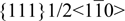
 ordinary slip, superlattice slip and twinning. The selective activation of the three types of deformation modes was confirmed to be achieved by compression tests of -
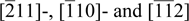
oriented single crystalline micropillars, respectively. The average CRSS values for ordinary slip, superlattice slip and deformation twinning obtained for micropillars with an initial side length between 3.8 and 7.9μm were estimated to be about 145, 284 and 113 MPa, respectively.
We study theoretical aspects of step fluctuations on vicinal surfaces by adding conservative white noise to the Burton-Cabrera-Frank model in one spatial dimension. We consider material deposition from above, as well as entropic and elastic-dipole step repulsions. Two approaches are discussed: (i) the linearization of stochastic equations when fluctuations are small, which captures correlations; and (ii) a mean field approach, which leaves out correlations but captures nonlinearities. Comparisons to kinetic Monte-Carlo simulations are presented.
High-level nuclear waste glasses are subject to radiation-induced degradation over very long time scales. In such glasses, bond-breakage and atom displacements occur by both radiolysis (principally from energetic beta-decay electrons) and ballistic mechanisms involving collision cascades initiated by energetic fission nuclei and recoil of alpha-emitting actinide nuclei [1]. This study investigates collision-cascade-induced alteration of the glass network in a simplified sodium borosilicate model nuclear waste glass, using molecular dynamics (MD) codes and efficient topological assessment algorithms. Collision cascades were initiated ballistically (4 keV initial kinetic energy, dissipated elastically) and carried out using MD codes incorporating both two-body Buckingham and three-body Stillinger-Weber potentials verified in the GULP atomistic simulation package. Network topologies of the initial and resulting altered glass structures were determined by enumerating the primitive-ring-based local cluster atom complement at each atom site. The topological description is seen to provide a revealing assessment of network structural changes in the simulated radiation environment that can be potentially related to observable macroscopic changes, such as swelling, viscosity changes, and radiation-induced devitrification.
Colloidal Au/Ag nanoparticles can be controllably assembled on anodic aluminum oxide (AAO) surfaces; monolayer coating on the membrane on AAO with smaller pores, or a nano-net arrangement along the edges of AAO with larger pores. The supported Au and Ag nanoparticles on the AAO membranes are closely packed and exhibited localized surface plasmon resonance (LSPR). Thus AAO membrane coated with Au or Ag nanoparticles is a highly surface-enhanced Raman scattering (SERS) active substrate. High quality SERS spectra were obtained using fullerene molecules C60 & C70 as the probe molecules and the filtered Au nanoparticles as the substrate. Furthermore, new SERS systems were obtained from Au nanoparticles assembled into the pores of AAO-supported fullerene nano-tubes, and the C60/C70 nano-tube arrays loaded with Au nanoparticles. The new SERS systems made use of the contributions from AAO, the LSPR of the Au nanoparticles, and a uniform assembly of the probe molecules in the nanostructures. These approaches have also been applied to small organic molecule systems using Ag nanoparticles.
Photonic integration has proved remarkably successful in combining multiple optical devices onto a single chip with the benefits of added functionality, and reduction in costs, arising from the replacement of manual assembly and alignment of individual components with lithographic techniques. However, the incorporation of optical isolators and related non-reciprocal devices within standard optoelectronic wafer platforms is exceptionally challenging. Preferred magneto-optic materials cannot be exploited as waveguide core layers on semiconductor wafers due to a lower refractive index. Another difficulty is the phase velocity mismatch as a consequence of the inherent structural birefringence associated with waveguide geometries.
Our approach to the integration of an optical isolator with a III-V semiconductor laser involves combining a nonreciprocal mode converter with a reciprocal mode converter, based on an asymmetric profiled rib waveguide, fabricated by Reactive Ion Etching. We demonstrate that suitably tapered waveguides can be employed to connect the mode converter to other sections thereby avoiding problems caused by mode-matching and reflections from the section interfaces.
The nonreciprocal mode converter is formed from a continuation of the III-V semiconductor waveguide core with a magneto-optic upper cladding so that Faraday rotation occurs through the interaction of the evanescent tail. The phase velocity mismatch due to the waveguide birefringence is overcome using a quasi-phase-matching approach. Lithography is used to pattern the top cladding so that the film immediately on top of the waveguide core alternates between magnetooptic and a non-magneto-optic dielectric of a similar refractive index. Our first demonstrations used a dielectric (silica or silicon nitride) patterned by etching, or lift-off, on top of a GaAs rib waveguide, over which was deposited a magneto-optic film. This film was deposited by sputtering from a Ce:YIG target and demonstrated magnetic hysteresis, but, as it was not annealed, it was believed to consist of Ce:YIG and/or gamma iron oxide microcrystallites embedded in an amorphous matrix. With quasi-phase-matching periods of 110–160 μm and a waveguide length of 8 mm, we were able to demonstrate up to 12% non-reciprocal TE- to TM-mode conversion around a wavelength of 1.3 μm using the remanent magnetisation.
In order to enhance the magneto-optic effect it is desirable to anneal such films. However the mismatch in thermal expansion coefficients results in a catastrophic failure of samples with large area film coverage. This problem has been shown to be alleviated by patterning the YIG film. Unfortunately wet-etching of YIG also etches (Al)GaAs and, therefore, the development of a lift-off process for YIG deposition has been undertaken. Initial results are promising with ∼100 μm×2.5 μm YIG sections deposited on a GaAs layer which remain intact after an anneal in an oxygen atmosphere.