Refine search
Actions for selected content:
106117 results in Materials Science
Ceramic-matrix composites take the heat
-
- Journal:
- MRS Bulletin / Volume 40 / Issue 11 / November 2015
- Published online by Cambridge University Press:
- 09 November 2015, pp. 916-918
- Print publication:
- November 2015
-
- Article
-
- You have access
- HTML
- Export citation
RESEARCH HIGHLIGHTS: Perovskites
-
- Journal:
- MRS Bulletin / Volume 40 / Issue 11 / November 2015
- Published online by Cambridge University Press:
- 09 November 2015, pp. 896-897
- Print publication:
- November 2015
-
- Article
-
- You have access
- HTML
- Export citation
Ni3TeO6 crystal structure exhibits interlocked chiral and polar domain walls
-
- Journal:
- MRS Bulletin / Volume 40 / Issue 11 / November 2015
- Published online by Cambridge University Press:
- 09 November 2015, pp. 899-900
- Print publication:
- November 2015
-
- Article
-
- You have access
- HTML
- Export citation
The Moore’s Law of Moore’sLaws
-
- Journal:
- MRS Bulletin / Volume 40 / Issue 11 / November 2015
- Published online by Cambridge University Press:
- 09 November 2015, pp. 991-992
- Print publication:
- November 2015
-
- Article
-
- You have access
- HTML
- Export citation
Progress in mesoscale science
-
- Journal:
- MRS Bulletin / Volume 40 / Issue 11 / November 2015
- Published online by Cambridge University Press:
- 09 November 2015, pp. 919-922
- Print publication:
- November 2015
-
- Article
-
- You have access
- HTML
- Export citation
White Paper: High-temperature FORC study of single- and multi-phase permanent magnets: LAKE SHORE CRYOTRONICS, INC.
-
- Journal:
- MRS Bulletin / Volume 40 / Issue 11 / November 2015
- Published online by Cambridge University Press:
- 09 November 2015, pp. 903-905
- Print publication:
- November 2015
-
- Article
-
- You have access
- HTML
- Export citation
Materials in Energy Conversion, Harvesting, and Storage Kathy Lu: Wiley, 2014 448 pages, $159.95 (e-book $127.99) ISBN 978-1-118-88910-7
-
- Journal:
- MRS Bulletin / Volume 40 / Issue 11 / November 2015
- Published online by Cambridge University Press:
- 09 November 2015, pp. 982-984
- Print publication:
- November 2015
-
- Article
-
- You have access
- HTML
- Export citation
Renewables push greenhouse gas emission savings in Europe: https://ec.europa.eu/jrc
-
- Journal:
- MRS Bulletin / Volume 40 / Issue 11 / November 2015
- Published online by Cambridge University Press:
- 09 November 2015, pp. 907-908
- Print publication:
- November 2015
-
- Article
-
- You have access
- HTML
- Export citation
CAREER CENTRAL
-
- Journal:
- MRS Bulletin / Volume 40 / Issue 11 / November 2015
- Published online by Cambridge University Press:
- 09 November 2015, pp. 985-990
- Print publication:
- November 2015
-
- Article
-
- You have access
- Export citation
Federal agencies announce materials data challenge: www.challenge.gov/challenge/materials-science-and-engineering-data-challenge
-
- Journal:
- MRS Bulletin / Volume 40 / Issue 11 / November 2015
- Published online by Cambridge University Press:
- 09 November 2015, pp. 906-907
- Print publication:
- November 2015
-
- Article
-
- You have access
- HTML
- Export citation
Meet Our Authors
-
- Journal:
- MRS Bulletin / Volume 40 / Issue 11 / November 2015
- Published online by Cambridge University Press:
- 09 November 2015, pp. 923-924
- Print publication:
- November 2015
-
- Article
-
- You have access
- HTML
- Export citation
Norway faces windy road to offshore wind
-
- Journal:
- MRS Bulletin / Volume 40 / Issue 11 / November 2015
- Published online by Cambridge University Press:
- 09 November 2015, pp. 914-915
- Print publication:
- November 2015
-
- Article
-
- You have access
- HTML
- Export citation
New materials are in vogue: thedesignjunction.co.uk
-
- Journal:
- MRS Bulletin / Volume 40 / Issue 11 / November 2015
- Published online by Cambridge University Press:
- 09 November 2015, pp. 909-912
- Print publication:
- November 2015
-
- Article
-
- You have access
- HTML
- Export citation
News and analysis on materials solutions to energy challenges: www.mrs.org/energy-quarterly
-
- Journal:
- MRS Bulletin / Volume 40 / Issue 11 / November 2015
- Published online by Cambridge University Press:
- 09 November 2015, p. 913
- Print publication:
- November 2015
-
- Article
-
- You have access
- HTML
- Export citation
Understanding materials microstructure and behavior at the mesoscale
-
- Journal:
- MRS Bulletin / Volume 40 / Issue 11 / November 2015
- Published online by Cambridge University Press:
- 09 November 2015, pp. 951-960
- Print publication:
- November 2015
-
- Article
- Export citation
MRS volume 40 issue 11 Cover and Front matter
-
- Journal:
- MRS Bulletin / Volume 40 / Issue 11 / November 2015
- Published online by Cambridge University Press:
- 09 November 2015, pp. f1-f6
- Print publication:
- November 2015
-
- Article
-
- You have access
- Export citation
Bio Focus: Gold nanoparticles enable instant colorimetric hydration sensor
-
- Journal:
- MRS Bulletin / Volume 40 / Issue 11 / November 2015
- Published online by Cambridge University Press:
- 09 November 2015, p. 899
- Print publication:
- November 2015
-
- Article
-
- You have access
- HTML
- Export citation
Nanomaterials under stress: A new opportunity for nanomaterials synthesis and engineering
-
- Journal:
- MRS Bulletin / Volume 40 / Issue 11 / November 2015
- Published online by Cambridge University Press:
- 09 November 2015, pp. 961-970
- Print publication:
- November 2015
-
- Article
- Export citation
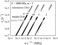
An efficient way of extracting creep properties from short-time spherical indentation tests
-
- Journal:
- Journal of Materials Research / Volume 30 / Issue 22 / 27 November 2015
- Published online by Cambridge University Press:
- 30 October 2015, pp. 3542-3552
- Print publication:
- 27 November 2015
-
- Article
- Export citation

Reduced hardening of nanocrystalline nickel under multiaxial indentation loading
-
- Journal:
- Journal of Materials Research / Volume 30 / Issue 22 / 27 November 2015
- Published online by Cambridge University Press:
- 30 October 2015, pp. 3528-3541
- Print publication:
- 27 November 2015
-
- Article
- Export citation
