


I. INTRODUCTION
Waveguide E- and H- plane junctions are widely used in modern antenna-feeder equipments working at microwave and extremely high frequencies [Reference Lewin1–Reference Widarta, Kuwano and Kokubun5]. Junction matching is usually carried out by inductive or capacitive diaphragms [Reference Abdelmonem, Yao and Zaki6, Reference Blas, Mira, Boria, Gimeno, Bressan and Arcioni7], and resonant metal rods [Reference Blas, Mira, Boria, Gimeno, Bressan and Arcioni7, Reference Wu and Wang8] in the straight waveguide. The rods are preferable, since they do not block the waveguide cross-section. In almost all publications on this topic, the rods were assumed to be perfectly conducting and located in the coupling area symmetrically with respect to the waveguide walls. In this paper, the first in literature, we consider the resonant coupling problem between an infinite rectangular waveguide, in which is located parallel to the narrow walls monopole with variable along their axis surface impedance, and a semi-infinite waveguide through a resonant slot in its end-wall. Also feature of the proposed junction design is monopole-slot coupling between the two waveguides of different cross-sections. Mathematical modeling plays an important role in the development of complex waveguide devices, since their experimental optimization is extremely time consuming, expensive, and sometimes impossible.
However, we must understand that a direct numerical analysis of the junction with any commercial software, such as Ansoft HFSS (high frequency structural simulator), is а complex and quite tedious problem. First, the analysis must be performed using an integrated approach, which should combine various software tools for computing characteristic of separate device fragments. Second, 3D rendering of the vibrator scatterer with variable surface impedance is a complicated problem. This is related to the fact that physical implementation of the vibrator with a predefined impedance distribution over its surface is a separate problem of design synthesis. Third, the usage of several discrete ports in coupling area of the slot that is necessary for multimode excitation of side waveguides requires a step-by-step design algorithm and additional analysis of its physical adequacy. Thus, the modeling of the waveguide junction using Ansoft HFSS package can be associated with both unreasonable costs of computer resources and long development time, so that it may become ineffective as compared with the proposed method based on the numerical and analytical solution of boundary value problem.
This paper is aimed at creating a mathematical model of the T-junction. The model is applied to study energy characteristics of the junction in the single-mode regime of both waveguides and to explore multi-mode excitation of the side semi-infinite waveguide, since this type of excitation is not yet sufficiently covered in the literature [Reference Wu and Wang8]. The electromagnetic problem of fundamental mode scattering in the straight waveguide is formulated and analytically solved by the well-proven generalized method of induced electro -magneto-motive forces (EMMF) [Reference Berdnik, Katrich, Nesterenko and Penkin9–Reference Berdnik, Katrich, Nesterenko, Penkin and Penkin12] in Section II. The energy characteristics of the junction obtained by modeling are presented in Section III. The overall results and some practical advice concerning designing the T-junctions are given in the Conclusion.
II. FORMULATION OF THE PROBLEM AND SOLUTION OF INTEGRAL EQUATIONS FOR THE CURRENTS
Let the fundamental wave TE 10 propagates in a hollow infinite rectangular waveguide with perfectly conducting walls (the area index is “Wg1”) from the region z = −∞. In the plane of the waveguide cross-section, a thin asymmetrical vibrator (monopole) with variable surface impedance, contacting with the waveguide wall, is placed parallel to the narrow waveguide walls. The waveguide dimension is {a × b}, the monopole radius is r and its length is L v ((r v /L v ) ≪ 1, (r/λ) ≪ 1, λ is wavelength in free space). A narrow transverse slot in the waveguide broad wall radiates into the hollow semi-infinite rectangular waveguide with cross section {a 2 × b 2} (the area index is “Wg2”). The slot is cut symmetrically relative to the line y 2 = b 2/2; the thickness, width and length of the slot are h, d, and 2L sl ([d/(2L sl )] ≪ 1, (d/λ) ≪ 1), respectively. Further we will use only one boundary condition for the magnetic field in the slot aperture, and take into account the wall thickness h of the waveguide section in which the slot is cut [Reference Nesterenko, Katrich, Penkin and Berdnik10]. Displacement of the monopole in the cross section relative to the waveguide narrow wall is x 0. The slot center is shifted at a distance x 01 relative to the narrow wall of the straight waveguide, and the slot center in the end-wall of the side waveguide is shifted at x 02. The distance between the monopole and slot axes is equal to z 0 (Fig. 1).

Fig. 1. The geometry of structure and notations.
If time dependence is ei ωt (ω is the circular frequency, t is time) the initial system of integral equations for the electric current on the monopole J v (s 1) and the equivalent magnetic current in the slot J sl (s 2), which in the framework of accepted approximations for electrically thin radiators are one-dimensional, can be written as [Reference Berdnik, Katrich, Nesterenko and Penkin9]
 $$\eqalign{\left( {\displaystyle{{d^2} \over {ds_1^2 }} + k^2} \right) & \int_{ - L_v}^{L_v} {J_v({{s}_1^{\prime}})G_{s_1}^{Wg1} (s_1,{{s}_1^{\prime}})d{{s}_1^{\prime}}} \cr &\quad - ik\int_{ - L_{sl}}^{L_{sl}} {J_{sl}({{s}_2^{\prime}})\tilde G_{s_2}^{Wg1} (s_1,{{s}_2^{\prime}})d{{s}_2^{\prime}}} \cr & = - i\omega \left[ {E_{0s_1}(s_1) - z_i(s_1)J_v(s_1)} \right],}$$
 $$\eqalign{\left( {\displaystyle{{d^2} \over {ds_2^2 }} + k^2} \right) & \int_{ - L_{sl}}^{L_{sl}} {J_{sl}({{s}_2^{\prime}})\left[ {G_{s_2}^{Wg1} (s_2,{{s}_2^{\prime}}) + G_{s_2}^{Wg2} (s_2,{{s}_2^{\prime}})} \right]d{{s}_2^{\prime}}} \cr &\quad - ik\int_{ - L_v}^{L_v} {J_v({{s}_1^{\prime}})\tilde G_{s_1}^{Wg1} (s_2,{{s}_1^{\prime}})d{{s}_1^{\prime}}} \cr & = - i\omega H_{0s_2}(s_2).}$$
Here s
1 and s
2 are local coordinates along the monopole and slot axes, respectively; z
i
(s
1) (Ω/m) is internal linear impedance of the monopole;
 $E_{0s_1} (s_1 )$
and
$E_{0s_1} (s_1 )$
and
 $H_{0s_2} (s_2 )$
are projections of the components of the H
10-wave field onto the monopole and slot axes, respectively;
$H_{0s_2} (s_2 )$
are projections of the components of the H
10-wave field onto the monopole and slot axes, respectively;
 $G_{s_1} ^{Wg1} (s_1, s'_1 )$
and
$G_{s_1} ^{Wg1} (s_1, s'_1 )$
and
 $G_{s_2} ^{Wg1,2} (s_2, s'_2 )$
are the Green's functions components of electric and magnetic type for the infinite and semi-infinite waveguides [Reference Nesterenko, Katrich, Penkin and Berdnik10, Reference Nesterenko, Katrich, Penkin, Dakhov and Berdnik11]; “−L
v
” is the coordinate of mirror image of the monopole end relative to the bottom broad wall of the straight waveguide [Reference Nesterenko, Katrich, Penkin, Dakhov and Berdnik11]; J
v
(±L
v
) = 0, J
sl
(±L
sl
) = 0;
$G_{s_2} ^{Wg1,2} (s_2, s'_2 )$
are the Green's functions components of electric and magnetic type for the infinite and semi-infinite waveguides [Reference Nesterenko, Katrich, Penkin and Berdnik10, Reference Nesterenko, Katrich, Penkin, Dakhov and Berdnik11]; “−L
v
” is the coordinate of mirror image of the monopole end relative to the bottom broad wall of the straight waveguide [Reference Nesterenko, Katrich, Penkin, Dakhov and Berdnik11]; J
v
(±L
v
) = 0, J
sl
(±L
sl
) = 0;
 $\tilde G_{s_1} ^{Wg1} (s_2, s'_1 ) = (\partial /\partial z)G_{s_1} ^{Wg1} [x(s_2 ),0,z;\,x'(s'_1 ),y'(s'_1 ),z_0 ]$
,
$\tilde G_{s_1} ^{Wg1} (s_2, s'_1 ) = (\partial /\partial z)G_{s_1} ^{Wg1} [x(s_2 ),0,z;\,x'(s'_1 ),y'(s'_1 ),z_0 ]$
,
 $\tilde G_{s_2} ^{Wg1} (s_1, s'_2 ) = (\partial /\partial z)G_{s_2} ^{Wg1} [x(s_1 ),y(s_1 ),z;\,x'(s'_2 ),0,0]$
under condition that z = 0 and z = z
0 are substituted respectively into
$\tilde G_{s_2} ^{Wg1} (s_1, s'_2 ) = (\partial /\partial z)G_{s_2} ^{Wg1} [x(s_1 ),y(s_1 ),z;\,x'(s'_2 ),0,0]$
under condition that z = 0 and z = z
0 are substituted respectively into
 $\tilde G_{s_1} ^{Wg1} $
and
$\tilde G_{s_1} ^{Wg1} $
and
 $\tilde G_{s_2} ^{Wg1} $
after derivation; k = 2π/λ.
$\tilde G_{s_2} ^{Wg1} $
after derivation; k = 2π/λ.
We will seek the solution of the equations system (1) by a generalized method of induced EMMF [Reference Berdnik, Katrich, Nesterenko and Penkin9–Reference Nesterenko, Katrich, Penkin, Dakhov and Berdnik11], using functions J v (s 1) = J 0v f v (s 1) and J sl (s 2) = J 0sl f sl (s 2) as approximating expressions for the currents. Here J 0v and J 0sl are unknown current amplitudes, f v (s 1) and f sl (s 2) are predetermined functions of the current distributions, which can be derived as the solution of equation (1) by the asymptotic averaging method for the solitary monopole and solitary slot under condition z 0 = 0 [Reference Nesterenko, Katrich, Penkin and Berdnik10, Reference Nesterenko, Katrich, Penkin, Dakhov and Berdnik11]. For our monopole-slot structure excited by the H 10 wave we have
 $$f_v (s_1 ) = \cos \tilde ks_1 - \cos \tilde kL_v,$$
 $$f_{sl} (s_2 ) = \cos ks_2 - \cos kL_{sl},$$
where
 $\tilde k = k - i2\pi z_i^{av} /(Z_0 \Omega )$
,
$\tilde k = k - i2\pi z_i^{av} /(Z_0 \Omega )$
,
 $z_i^{av} = 1/(2L_v )\int_{ - L_v} ^{L_v} {z_i (s_1 )ds_1} $
is the average value of the internal impedance along the monopole length [Reference Nesterenko, Katrich, Penkin, Dakhov and Berdnik11], Z
0 = 120π Ω, Ω = 2ln(2L
v
/r). Then we multiply the equations (1a) and (1b) by the functions f
v
(s
1) and f
sl
(s
2), respectively, and integrate the equation (1a) along the length of the monopole and equation (1b) along the length of the slot. Thus, we obtain a system of linear algebraic equations whose solution is the currents amplitudes J
0v
, J
0sl
$z_i^{av} = 1/(2L_v )\int_{ - L_v} ^{L_v} {z_i (s_1 )ds_1} $
is the average value of the internal impedance along the monopole length [Reference Nesterenko, Katrich, Penkin, Dakhov and Berdnik11], Z
0 = 120π Ω, Ω = 2ln(2L
v
/r). Then we multiply the equations (1a) and (1b) by the functions f
v
(s
1) and f
sl
(s
2), respectively, and integrate the equation (1a) along the length of the monopole and equation (1b) along the length of the slot. Thus, we obtain a system of linear algebraic equations whose solution is the currents amplitudes J
0v
, J
0sl
 $$\eqalign{J_{0v} (Z_{11} + F_z ) + J_{0sl} Z_{12} = & -\! i\omega /(2k)E_1, \cr J_{0sl} (Z_{22}^{Wg1} + Z_{22}^{Wg2} ) + J_{0v} Z_{21} = & -\! i\omega /(2k)H_2.} $$
Here
 $$\eqalign{Z_{11} = & \displaystyle{{4\pi } \over {ab}}\sum\limits_{m = 1}^\infty {\sum\limits_{n = 0}^\infty {\left[ {\displaystyle{{\varepsilon _n(k^2 - k_y^2 ){\tilde k}^2} \over {kk_z{({\tilde k}^2 - k_y^2 )}^2}}} \right.} } e^{ - k_zr} \cr & \sin ^2k_xx_0\left. {{\left[ {\sin \tilde kL_v\cos k_yL_v - (\tilde k/k_y)\cos \tilde kL_v\sin k_yL_v} \right]}^2} \right],\cr&{\hskip-30pt} Z_{12} = Z_{21} = \displaystyle{{4\pi } \over {ab}}\sum\limits_{m = 1}^\infty \sum\limits_{n = 0}^\infty \left[ {\displaystyle{{\varepsilon _nk\tilde ke^{ - k_zz_0}} \over {i(k^2 - k_x^2 )({\tilde k}^2 - k_y^2 )}}} \right. \sin k_xx_0\sin k_xx_{01} \cr &\quad\times \left[ {\sin \tilde kL_v\cos k_yL_v - (\tilde k/k_y)\cos \tilde kL_v\sin k_yL_v} \right] \cr & \quad \left. \times\, \left[ {\sin kL_{sl}\cos k_xL_{sl} - (k/k_x)\cos kL_{sl}\sin k_xL_{sl}} \right] \vphantom{\displaystyle{{8\pi^2 } \over {ab^2}}} \right], \cr Z_{22}^{Wg1} = & \displaystyle{{8\pi } \over {ab}}\sum\limits_{m = 1}^\infty {\sum\limits_{n = 0}^\infty {\left[ {\displaystyle{{\varepsilon _nke^{ - k_z(d_e/4)}} \over {k_z(k^2 - k_x^2 )}}} \right.} } \sin ^2k_xx_{01} \cr & \left. {\mathop {{\left[ {\sin kL_{sl}\cos k_xL_{sl} - (k/k_x)\cos kL_{sl}\sin k_xL_{sl}} \right]}^2}\limits_{} } \right], \cr Z_{22}^{Wg2} = & \displaystyle{{16\pi } \over {ab}}\sum\limits_{m = 1}^\infty {\sum\limits_{n = 0}^\infty {\left[ {\displaystyle{{\varepsilon _nk} \over {k_z(k^2 - k_x^2 )}}} \right.} } \sin ^2k_xx_{02} \cos k_yy_0\cos k_y\cr & \!\!\!\!\!\left( {y_0 + \displaystyle{{d_e} \over 4}} \right) \left. {{\left[ {\sin kL_{sl}\cos k_xL_{sl} - (k/k_x)\cos kL_{sl}\sin k_xL_{sl}} \right]}^2} \right], \cr Z_{22}^\Sigma = & Z_{22}^{Wg1} + Z_{22}^{Wg2} ;}$$
 $$\,\eqalign{E_1 &= 2H_0\left[ {k/(k_g\tilde k)} \right]\sin (\pi x_0/a)e^{ - ik_gz_0}f(\tilde kL_v), \cr f(\tilde kL_v) &= \sin \tilde kL_v - \tilde kL_v\cos \tilde kL_v, \cr H_2 &= 2H_0(1/k)\sin (\pi x_{01}/a)f(kL_{sl}), \cr f(kL_{sl}) &= \displaystyle{{\sin kL_{sl}\cos (\pi L_{sl}/a) - (ka/\pi )\cos kL_{sl}\sin (\pi L_{sl}/a)} \over {1 - {[\pi /(ka)]}^2}}, \cr F_z &= - \displaystyle{i \over r}\int_0^{L_v} {f_v^2 (s_1){\bar Z}_{SV}(s_1){\rm d}s_1} .}$$
In the formulas (4) and (5)
 $\varepsilon _n = \left\{ \matrix{1,\;n = 0 \hfill \cr 2,\;n \ne 0 \hfill} \right.$
, k
x
= mπ/a(a
2), k
y
= nπ/b(b
2),
$\varepsilon _n = \left\{ \matrix{1,\;n = 0 \hfill \cr 2,\;n \ne 0 \hfill} \right.$
, k
x
= mπ/a(a
2), k
y
= nπ/b(b
2),
 $k_z = \sqrt {k_x^2 + k_y^2 - k^2} $
,
$k_z = \sqrt {k_x^2 + k_y^2 - k^2} $
,
 $k_g = \sqrt {k^2 - (\pi /a)^2} $
, m and n are integers;
$k_g = \sqrt {k^2 - (\pi /a)^2} $
, m and n are integers;
 $\bar Z_S (s_1 ) = \bar R_S + i\bar X_S {\rm \phi} (s_1 )$
is the distributed surface impedance normalized to Z
0
$\bar Z_S (s_1 ) = \bar R_S + i\bar X_S {\rm \phi} (s_1 )$
is the distributed surface impedance normalized to Z
0
 $\bar Z_S (s_1 ) = 2\pi rz_i (s_1 )$
, ϕ(s
1) is the given function, d
e
= d exp(−πh/2d) is equivalent slot width [Reference Berdnik, Katrich, Nesterenko and Penkin9], which take into account the actual wall thickness h of the waveguide.
$\bar Z_S (s_1 ) = 2\pi rz_i (s_1 )$
, ϕ(s
1) is the given function, d
e
= d exp(−πh/2d) is equivalent slot width [Reference Berdnik, Katrich, Nesterenko and Penkin9], which take into account the actual wall thickness h of the waveguide.
Solution of the equation system (3) can be written as
 $$\eqalign{J_{0v} = & - \displaystyle{{i\omega} \over {2k}}\displaystyle{{E_1 Z_{22}^\Sigma - H_2 Z_{12}} \over {(Z_{11} + F_z )Z_{22}^\Sigma - Z_{21} Z_{12}}} = - \displaystyle{{i\omega H_0} \over {k^2}} J_v, \cr J_{0sl} = & - \displaystyle{{i\omega} \over {2k}}\displaystyle{{H_2 (Z_{11} + F_z ) - E_1 Z_{21}} \over {(Z_{11} + F_z )Z_{22}^\Sigma - Z_{21} Z_{12}}} = - \displaystyle{{i\omega H_0} \over {k^2}} J_{sl}.} $$
The currents on the monopole and in the slot can be obtained using (2) and (6)
 $$\eqalign{J_v (s_1 ) = & -\! H_0 (i\omega /k^2 )J_v (\cos \tilde ks_1 - \cos \tilde kL_v ), \cr J_{sl} (s_2 ) = & -\! H_0 (i\omega /k^2 )J_{sl} (\cos ks_2 - \cos kL_{sl} ),} $$
where H 0 is the amplitude of TE 10 wave. The reflection and transmission coefficients, S 11 and S 21 in the straight waveguide can be represented as
 $$\eqalign{S_{11} =& \displaystyle{{4\pi i} \over {abk}}\left\{ \displaystyle{{2k_g} \over k}J_{sl} \sin \displaystyle{{\pi x_{01}} \over a}f(kL_{sl} ) \right. \cr & \left. { - \displaystyle{k \over {\tilde k}}J_v \sin \displaystyle{{\pi x_0} \over a}e^{ - ik_g z_0} f(\tilde kL_v )} \right\}e^{2ik_g z},} $$
 $$\eqalign{S_{21} = &1 + \displaystyle{{4\pi i} \over {abk}}\left\{ {\displaystyle{{2k_g} \over k}J_{sl} \sin \displaystyle{{\pi x_{01}} \over a}f(kL_{sl} )} \right. \cr &+ \left. {\displaystyle{k \over {\tilde k}}J_v \sin \displaystyle{{\pi x_0} \over a}e^{ik_g z_0} f(\tilde kL_v )} \right\}}.$$
The number of propagating wave modes M in the side waveguide section Wg2 depends upon the dimensions of the waveguide cross section {a
2 × b
2}. Therefore, the scattering matrix of the waveguide junction contains the power reflection and transmission coefficient P
11 = |S
11|2, P
21 = |S
21|2 for the propagating mode in the straight waveguide and a number of power transmission coefficients
 $P_{31}^{mn} $
for the propagating modes in the side waveguide. The coefficients
$P_{31}^{mn} $
for the propagating modes in the side waveguide. The coefficients
 $P_{31}^{mn} $
are determined by the formula
$P_{31}^{mn} $
are determined by the formula
 $P_{31}^{mn} = P_{31} (P_{sl}^{mn} /P_{\Sigma sl}^{mn} )$
, where P
31 = 1 − P
11 − P
21 − P
σv
,
$P_{31}^{mn} = P_{31} (P_{sl}^{mn} /P_{\Sigma sl}^{mn} )$
, where P
31 = 1 − P
11 − P
21 − P
σv
,
 $(P_{sl}^{mn} /P_{\Sigma sl}^{mn} )$
is the power ratio of the partial waves to the total power of waves propagating in the arm Wg2, normalized to the power of the wave TE
10 coming from the generator, P
σv
is the power loss in the monopole, which can be determined using the energy balance equation P
11v
+ P
21v
+ P
σv
= 1 for the auxiliary problem with the slot metallization. For asymmetric waveguides junctions (Fig. 1) under conditions y
0 = b
2/2, the expression for the magnetic type wave propagating in the side waveguide arm can be presented as
$(P_{sl}^{mn} /P_{\Sigma sl}^{mn} )$
is the power ratio of the partial waves to the total power of waves propagating in the arm Wg2, normalized to the power of the wave TE
10 coming from the generator, P
σv
is the power loss in the monopole, which can be determined using the energy balance equation P
11v
+ P
21v
+ P
σv
= 1 for the auxiliary problem with the slot metallization. For asymmetric waveguides junctions (Fig. 1) under conditions y
0 = b
2/2, the expression for the magnetic type wave propagating in the side waveguide arm can be presented as
 $$P_{sl}^{m0} = \displaystyle{{a_2 b_2 k_g} \over {abk_g^{m0}}} \left \vert {\displaystyle{{16\pi k_g^{m0} \sin (\pi x_{01} /a)f(kL_{sl} )\sin (m\pi x_{02} /a_2 )f_{sl}^{m0}} \over {a_2 b_2 k^3 Z_{22}^\Sigma}}} \right \vert ^2, $$
where
 $$\eqalign{&f_{sl}^{m0} =\cr&\quad \displaystyle{{\sin kL_{sl} \cos (m\pi L_{sl} /a_2 ) - (ka_2 /m\pi )\cos kL_{sl} \sin (m\pi L_{sl} /a_2 )} \over {1 - [m\pi /(ka_2 )]^2}},} $$
 $$k_g^{m0} = \sqrt {k^2 - (m\pi /a)^2} $
and
 $$P_{\Sigma sl}^{m0} = \sum\limits_{m = 1}^M {P_{sl}^{m0}}. $$
It is known [Reference Nesterenko, Katrich, Penkin, Dakhov and Berdnik11] that the impedance vibrators can be tuned to resonance if its length is less than that of the perfectly conducting vibrators and the surface impedance of the inductive type (
 ${\bar X}_S$
> 0) is used. If a junction works at large power, the electrical breakdown can occur between the monopole end and waveguide wall. Therefore, it is appropriate to employ inductive surface impedance. All modeling results presented below were obtained using surface impedance distributed along the monopole axis according to functions: constant ϕ0 (s
1) = 1 and cosine ϕ1 (s
1) = (π/2) cosπs
1/2L
v
distribution functions. If the constant distribution function is used, the expression (5) has the form
${\bar X}_S$
> 0) is used. If a junction works at large power, the electrical breakdown can occur between the monopole end and waveguide wall. Therefore, it is appropriate to employ inductive surface impedance. All modeling results presented below were obtained using surface impedance distributed along the monopole axis according to functions: constant ϕ0 (s
1) = 1 and cosine ϕ1 (s
1) = (π/2) cosπs
1/2L
v
distribution functions. If the constant distribution function is used, the expression (5) has the form
 $$\eqalign{F_z^{{\rm \phi} _0} &= - \displaystyle{{iL_v (\bar R_S + i\bar X_S )} \over {2r}}\left[ {(2 + \cos 2\tilde kL_v ) - 3\displaystyle{{\sin 2\tilde kL_v} \over {2\tilde kL_v}}} \right] \cr &= F_z^c (\bar R_{SV} + i\bar X_{SV} )\Phi _z^c.}$$
For the cosine function we have
 $$\eqalign{F_z^{{\rm \phi} _1} = & F_z^c \left\{ {\mathop {\bar R_S \Phi _z^c} \limits_{}^{}} \right. + i\bar X_S \left[ {\displaystyle{{\pi ^2 \cos 2\tilde kL_v} \over {\pi ^2 - (4\tilde kL_v )^2}}} \right. \cr & - \left. {\left. {2\cos \tilde kL_v \displaystyle{{\pi ^2 + (2\tilde kL_v )^2} \over {\pi ^2 - (2\tilde kL_v )^2}} + 1} \right]} \right\}.}$$
Formulas for surface impedances of thin vibrators, obtained by the authors in the framework of the impedance concept are given in [Reference Nesterenko, Katrich, Penkin, Dakhov and Berdnik11].
III. NUMERICAL RESULTS
Our mathematical model allows effective computation of the energy characteristics for waveguide junctions both with and without the monopole. The program base on the model is by several orders of magnitude faster than commercial software. The program base on the model is by several orders of magnitude faster than any commercial software. In our approximation, the inequalities 2r v /L v ≤ 1 and [d/(2L sl )] hold, and the numbers of terms in double series (4) was chosen to provide the calculation of the matrix coefficients in each of the coupling areas with an accuracy of 0.1%.
Figure 2 shows the junction energy characteristics versus the wavelength, P
q1, q = 1, 2, 3, for the solitary slot without the monopole used for coupling between the infinite and semi-infinite single-mode waveguides. All computations were performed using the following geometrical parameters of the structure: a = 58, b = 25, d = 4, h = 0.5, r = 2 mm, x
0 = a/8, y
0 = b
2/2. As can be seen, the powers of waves transmitted into arms 2 and 3 are equal if the slot resonant wavelength is
 $\lambda _{sl}^{res} \approx 80\,\; {\rm mm}$
amounting up to 90% of the incident wave power. About 10% of the incident power is reflected back to the generator. The slot length is chosen so that its resonant wavelength is in the middle of the operating waveband. The general theory of slot radiators predicts three features of the junction structure: (1) no more than 50% of the incident wave power can be directed into the side waveguide, and the power can be divided in the range
$\lambda _{sl}^{res} \approx 80\,\; {\rm mm}$
amounting up to 90% of the incident wave power. About 10% of the incident power is reflected back to the generator. The slot length is chosen so that its resonant wavelength is in the middle of the operating waveband. The general theory of slot radiators predicts three features of the junction structure: (1) no more than 50% of the incident wave power can be directed into the side waveguide, and the power can be divided in the range
 $(1/6) \le P_{31}^{10} /P_{21} \le 1$
by selection of the operating wavelength; (2) the power division between the arms in the ratio 1:1 can be achieved only at the slot resonant wavelength when the highest reflection is observed in the straight waveguide; (3) resonant coupling of the waveguides determines the relative band limitedness as compared with bridge-type junctions for any mode of power division between the arms. The first two restrictions can be eliminated by introducing the impedance monopole in the straight waveguide near the slot. Indeed, if a monopole with a constant impedance is placed at the distance
$(1/6) \le P_{31}^{10} /P_{21} \le 1$
by selection of the operating wavelength; (2) the power division between the arms in the ratio 1:1 can be achieved only at the slot resonant wavelength when the highest reflection is observed in the straight waveguide; (3) resonant coupling of the waveguides determines the relative band limitedness as compared with bridge-type junctions for any mode of power division between the arms. The first two restrictions can be eliminated by introducing the impedance monopole in the straight waveguide near the slot. Indeed, if a monopole with a constant impedance is placed at the distance
 $z_0 = \lambda _G^{Sres} /2$
(here
$z_0 = \lambda _G^{Sres} /2$
(here
 $\lambda _G^{Sres} = 2\pi /\sqrt {(2\pi /\lambda _{sl}^{res} )^2 - (\pi /a)^2} $
) from the slot longitudinal axis a significant increase in the power of the transmitted wave in the arm 3 (up to 90%) and decrease P
21 и P
11 is observed at resonant wavelength of the slot and monopole
$\lambda _G^{Sres} = 2\pi /\sqrt {(2\pi /\lambda _{sl}^{res} )^2 - (\pi /a)^2} $
) from the slot longitudinal axis a significant increase in the power of the transmitted wave in the arm 3 (up to 90%) and decrease P
21 и P
11 is observed at resonant wavelength of the slot and monopole
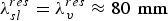 $\lambda _{sl}^{res} = \lambda _v^{res} \approx 80\,\; {\rm mm}$
(Fig. 3(a), z
0 = 54 mm). It is also possible to divide power of the transmitted waves in a predetermined ratio at certain wavelengths of operating band (in the range 60 ÷ 80 mm) with a sufficiently satisfactory arm matching. Figures 3(b) and 3(c) show the energy characteristics of the monopole, which length is L
v
= 15 mm. These characteristics coincide with that of the monopole in Fig. 3(a), but have different resonant wavelengths: (b)
$\lambda _{sl}^{res} = \lambda _v^{res} \approx 80\,\; {\rm mm}$
(Fig. 3(a), z
0 = 54 mm). It is also possible to divide power of the transmitted waves in a predetermined ratio at certain wavelengths of operating band (in the range 60 ÷ 80 mm) with a sufficiently satisfactory arm matching. Figures 3(b) and 3(c) show the energy characteristics of the monopole, which length is L
v
= 15 mm. These characteristics coincide with that of the monopole in Fig. 3(a), but have different resonant wavelengths: (b)
 $\lambda _v^{res} \approx 72\,\; {\rm mm}$
(perfectly conducting monopole), (c)
$\lambda _v^{res} \approx 72\,\; {\rm mm}$
(perfectly conducting monopole), (c)
 $\lambda _v^{res} \approx 88\,\; {\rm mm}$
(monopole with variable impedance). In these cases, the power of the transmitted waves can be divided in predefined ratio at some wavelengths in the operating waveband
$\lambda _v^{res} \approx 88\,\; {\rm mm}$
(monopole with variable impedance). In these cases, the power of the transmitted waves can be divided in predefined ratio at some wavelengths in the operating waveband
 $73 \div 100\; \,{\rm mm}$
(see Figs 3(b) and 3(c)) with satisfactory matching in the arm 1 (voltage standing wave ratio, VSWR ~ 2.0).
$73 \div 100\; \,{\rm mm}$
(see Figs 3(b) and 3(c)) with satisfactory matching in the arm 1 (voltage standing wave ratio, VSWR ~ 2.0).

Fig. 2. The energy characteristics versus wavelength for the solitary slot: b 2 = b, x 01 = x 02 = a/2.

Fig. 3. The energy characteristics versus wavelength for the slot-monopole system: b 2 = b, z 0 = 54 mm, x 01 = x 02 = a/2.
The revealed physical mechanisms were confirmed by experimental results for the monopole with variable impedance and are shown in Fig. 4, where the picture of experimental monopole model is also shown. The experimental model have been made in the form of corrugated brass rod with the crests thickness 1 mm, the notch width 1 mm, and the inner radius r i (s v ) = r exp[−ln (4.0)ϕ1 (s v )]. Here, as in other cases of the comparative analysis [Reference Berdnik, Katrich, Nesterenko and Penkin9–Reference Berdnik, Katrich, Nesterenko, Penkin and Penkin12], the design characteristics of the slot and vibrator-slot waveguide structures obtained by the generalized EMMF method differ from experimental data by no more than 2–5%. Note that the maximum difference is observed if distances z 0 between the vibrator and slot is of order of several slot widths d. This can be explained by scattering of cross-polarization fields on joint elements.

Fig. 4. The energy characteristics versus wavelength for the slot-monopole system: b 2 = b, z 0 = 54 mm, x 01,2 = a/2, (circles ‒ experimental data).
The possibility of transferring most of the incident power from the straight waveguide into the side waveguide can be used to organize additional modal channels of power division in the side waveguide. The regimes of equal power division between the separate modes in the side arm of the waveguide structure and between all the physical channels of the power division are of particular interest for practical applications.
Our calculations have shown that such regimes can be realized. Thus, if the size of the side waveguide broad wall is increased 2 times, the TE
10 and TE
20 waves are efficiently excited (Fig. 5) while the amplitude of TE
30 wave is negligibly small. A roughly equal division of power between the transmitted waves TE
10 and TE
20 in the wavelength band λ ∈ [93, 98.5] mm can be achieved by varying the monopole surface impedance and slot length. At the wavelength of 95 mm 90% of the incident power is transmitted from the straight waveguide into the side arm at the optimum matching and equal division of power between the excited modes (
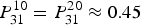 $P_{31}^{10} = P_{31}^{20} \approx 0.45$
). At wavelengths of 92.5 and 97.5 mm the regime of equal division among all the physical channels is observed (
$P_{31}^{10} = P_{31}^{20} \approx 0.45$
). At wavelengths of 92.5 and 97.5 mm the regime of equal division among all the physical channels is observed (
 $P_{21} = P_{31}^{10} = P_{31}^{20} \approx 0.3$
).
$P_{21} = P_{31}^{10} = P_{31}^{20} \approx 0.3$
).

Fig. 5. The energy characteristics versus wavelength for the slot-monopole system: b 2 = b, z 0 = 85 mm, x 01 = a/2, x 02 = a 2/4.
These trends of the power division are also observed when the waveguide side walls are decreased in order to reduce weight and dimensions of waveguide structures. In this case, it is possible to implement the regime of equal power division at shorter wavelengths. For example, if the side wall of the waveguide is reduced by 50%, the powers
 $P_{31}^{10} $
and
$P_{31}^{10} $
and
 $P_{31}^{20} $
are approximately equal in the waveband λ ∈ [69, 74] and are divided in various ratios with P
21 (Fig. 6). At the resonant wavelengths of the monopole and slot,
$P_{31}^{20} $
are approximately equal in the waveband λ ∈ [69, 74] and are divided in various ratios with P
21 (Fig. 6). At the resonant wavelengths of the monopole and slot,
 $\lambda _v^{res} = \lambda _{sl}^{res} \approx 71.5{\kern 1pt} \; \,{\rm mm}$
the reflection coefficient in the straight waveguide is almost zero, and 90% of the incident power transmitted into the side waveguide arm is equally divided between propagating modes,
$\lambda _v^{res} = \lambda _{sl}^{res} \approx 71.5{\kern 1pt} \; \,{\rm mm}$
the reflection coefficient in the straight waveguide is almost zero, and 90% of the incident power transmitted into the side waveguide arm is equally divided between propagating modes,
 $P_{31}^{10} = P_{31}^{20} \approx 0.45$
.
$P_{31}^{10} = P_{31}^{20} \approx 0.45$
.

Fig. 6. The energy characteristics versus wavelength for the slot-monopole system: z 0 = 46 mm, x 01 = a/2, x 02 = a 2/4.
If the slot length is reduced and the slot center is shifted to the narrow wall of the straight waveguide at x
01 = a/3, then x
02 = a
2/6, and the slot center is located at the antinode of the TE
30 wave, the wave TE
30 along with the waves TE
10 and TE
20 will effectively be excited in the side waveguide (Fig. 7). The coefficients
 $P_{31}^{10} $
and
$P_{31}^{10} $
and
 $P_{31}^{30} $
in the middle of the band are almost equal. These coefficients equal to P
21 at two wavelengths, and the coefficient
$P_{31}^{30} $
in the middle of the band are almost equal. These coefficients equal to P
21 at two wavelengths, and the coefficient
 $P_{31}^{20} $
is almost twice greater than P
21. At the resonant frequency, ratio
$P_{31}^{20} $
is almost twice greater than P
21. At the resonant frequency, ratio
 $P_{31}^{20} \approx P_{31}^{10} + P_{31}^{30} $
holds.
$P_{31}^{20} \approx P_{31}^{10} + P_{31}^{30} $
holds.

Fig. 7. The energy characteristics versus wavelength for the slot-monopole system: b 2 = b, z 0 = 46 mm, x 01 = a/3, x 02 = a 2/6.
IV. CONCLUSION
The energy characteristics of the E-plane T-junction for the rectangular waveguides were obtained by the mathematical modeling carried out on the basis of the analytical solution of the internal diffraction problem by the generalized method of induced EMMF. The system consisting of the impedance monopole in the infinite waveguide and the slot in the end-wall of the semi-infinite waveguide section is placed in the coupling area of the junction. The validity of the simulation results and the physical correctness of the approximations used for the problem solution is confirmed experimentally. Also note that the energy parameters of waveguide structures with a single slot and a perfectly conducting vibrator (not represented here graphically) obtained by the generalized method of induced EMMF and by the commercial software Ansoft HFSS are in good agreement.
As opposed to bridge-type junctions, the proposed construction is a resonant narrow-band device. Therefore, the waveguide structures of this type for a long time were not very interesting for the researchers. At present, multi-function devices are widely used in many practical applications, therefore the interest in such structures begins to grow. Particular attention is drawn to junctions functioning in multimode regime of power division, which allows controlling of this process. It has been shown that it is possible to achieve the division of power between the junction coupling arms and modes of propagating waves in a wide range by changing the geometric dimensions of the junction elements, surface impedance, and the distribution function of the surface impedance along the monopole. The present solution of the problem without much difficulty can be extended to multi-element vibrator-slot structures [Reference Berdnik, Katrich, Nesterenko, Penkin and Penkin12].
 Sergey L. Berdnik received the degree (similar to M.S.) in Radiophysics and Electronics from V. N. Karazin Kharkiv National University, Kharkiv, Ukraine in 2000, and received his Ph.D. degree in 2010. From 2000 he has been a research worker and Assistant Professor with the Department of Radiophysics, V. N. Karazin Kharkiv National University. Нe is currently an Associate Professor, also part-time Senior Researcher. His research interests include electromagnetic theory, diffraction's problems in applied electrodynamics, theory of waveguide-slot coupling elements and antennas array, theory of thin impedance vibrators and their arrays.
 Victor A. Katrich was born in Kharkiv, Ukrainian SSR, on September 18, 1944. He received the degree (similar to M.S.) in Radiophysics and Electronics from M. Gorky Kharkiv State University, Kharkov, Ukraine in 1968, and the Ph.D. degree in 1981. Since 1968 he has been with the M. Gorky Kharkiv State University (now V. N. Karazin Kharkiv National University). Since 1981 he has been Senior Researcher at the Department of Radiophysics. From 2005 until now he is Full Professor, also part-time Principle Scientist. His research interests include electromagnetic theory, diffraction's problems in applied electrodynamics, theory of the waveguide-slot coupling elements, theory of radiation of the arbitrary length slots and curvilinear slots cut in walls of the single-mode and poly-modal waveguides.
 Mikhail V. Nesterenko was born in Tallinn, Estonian SSR, on February 3, 1957. He received the degree (similar to M.S.) in Radiophysics and Electronics from M. Gorky Kharkiv State University, Kharkov, Ukraine in 1979, and the Ph.D. degree in 1989. Since 1979 he has been with the M. Gorky Kharkiv State University (now V. N. Karazin Kharkiv National University). Since 1989 he has been Senior Researcher at the Department of Radiophysics. From 2012 until now he is Doctor of Science and the Principle Scientist. His research interests include electromagnetic theory, diffraction's problems in applied electrodynamics, theory of thin impedance vibrators and their arrays, theory of waveguide-slot coupling elements.
 Yuriy M. Penkin was born in Kharkiv, Ukrainian SSR, on July 29, 1960. He received the degree (similar to M.S.) in Radiophysics and Electronics from M. Gorky Kharkiv State University, Kharkiv, Ukraine in 1982, and the Ph.D. degree in 1988. Since 1982 he has been with the M. Gorky Kharkiv State University (now V. N. Karazin Kharkiv National University). Since 1988 he has been Senior Researcher at the Department of Radiophysics. From 2002 until now he is Full Professor, also part-time Senior Researcher. His research interests include electromagnetic theory, diffraction's problems in applied electrodynamics, theory of the waveguide-slot coupling elements and theory of the excitation of electromagnetic waves in volumes with curvilinear coordinate boundaries.


