


Introduction
In modern microwave system, power dividers (PDs) [Reference Burdin, Podevin and Ferrari1] are widely applied in power amplifiers, antenna arrays, mixers, and phase shifters. Bandpass filters are also essential devices in radio frequency and microwave front ends. Conventionally, the PDs and bandpass filters are usually cascaded to provide signals splitting and filtering performances simultaneously. However, the cascades of PDs and bandpass filters will lead to relative high insertion losses and bulky circuit sizes. To overcome such shortcomings, filtering PDs have been investigated in [Reference Karimi, Siahkamari and Hamedani2–Reference Tang and Chen19] which can achieve signals splitting and filtering performances simultaneously in only one device.
In addition, wide upper stopband frequency range with deep rejection level is greatly demanded to suppress the out-of-band interferences, i.e. background noises and intermodulation signals from non-linear components, which commonly exist in modern communication system. Recently, some narrowband PDs with high passband selectivities and good out-of-band rejection performances are proposed in [Reference Karimi, Siahkamari and Hamedani2–Reference Song, Zhou, Fan, Zhu and Fan9]. In [Reference Karimi, Siahkamari and Hamedani2], a low-pass filter is inserted into the PD to realize harmonic suppression. Stub resonators introduced in [Reference Zhang, Wang and Hu3–Reference Danaeian, Moznebi, Afrooz and Hakimi5] and composite right-/left-handed transmission line (TL) structures employed in [Reference Ren, Song, Hu and Chen6] could generate transmission zeros (TZs), resulting in filtering responses and wide upper stopband ranges with high attenuations. In [Reference Song, Ren, Chen and Fan7–Reference Song, Zhou, Fan, Zhu and Fan9], filtering PDs with good out-of-band rejection performances have been designed based on coupling structures. Unfortunately, the 3 dB fractional bandwidths (BWs) of the PDs mentioned in [Reference Karimi, Siahkamari and Hamedani2–Reference Song, Zhou, Fan, Zhu and Fan9] are all <12%, which makes them not suitable for wideband communication systems.
With the development of wideband communication systems, it is essential to enhance the BW of filtering PDs. Some wideband filtering PDs (WFPDs) have been presented in [Reference Wang, Wang and Zhang10–Reference Tang and Chen19]. Coupling topology between a quarter-wavelength short-ended microstrip TL and two multimode resonators is introduced in [Reference Wang, Wang and Zhang10] to design WFPD with the 3 dB fractional BW of 32.1%. In [Reference Wong and Zhu11], a WFPD with 3 dB fractional BW of 109.5% is achieved by adopting parallel-coupled lines and a pair of quarter-wavelength short-circuited stubs. Periodic butterfly radial slots are etched on top layer of substrate-integrated waveguide in [Reference Chen, Zhang and Yu12] to realize a WFPD with 3 dB fractional BW of 44.4%. In [Reference Chen, Zhang and Yu12], the upper stopband extends to 1.78f 0 with the attenuation of 26 dB, which is the best out-of-band rejection performance among the WFPDs presented in [Reference Wang, Wang and Zhang10–Reference Chen, Zhang and Yu12]. However, the poor out-of-band rejection performance will limit the application of such devices in multi-standard wireless communication systems. Some efforts [Reference Tang, Lin, Fan and Song13–Reference Tang and Chen19] have also been made to design wideband PDs (WPDs) with filtering responses, wide upper-stopband range as well as deep rejection levels. In [Reference Tang, Lin, Fan and Song13], by replacing quarter-wavelength TLs in conventional Wilkinson PD with filters, a WPD with passband selectivity and harmonic suppression performances is realized. Coupled lines and loading terminations are adopted in [Reference Gao, Feng, Che and Xue14–Reference Tang and Chen19] to design WPDs with filtering responses and good out-of-band rejection performances. The WPD proposed in [Reference Tang and Chen19] achieves the best out-of-band rejection performance among the structures presented in [Reference Wang, Wang and Zhang10–Reference Tang and Chen19], where the upper stopband extends to 5.0f 0 with a rejection level of 17.2 dB. However, the passband selectivity of WPD proposed in [Reference Tang and Chen19] needs to be further enhanced. The WPDs in [Reference Tang, Lin, Fan and Song13–Reference Moradi, Moznebi, Afrooz and Movahhedi18] have high passband selectivity performances, but the harmonic suppression performances should be further improved.
In this paper, a series of novel wideband PDs with various TL sections and loading terminations is proposed to realize high passband selectivities and good out-of-band rejection performances. The operating mechanisms of the basic WFPD circuit are explained in detail based on the even-odd mode method. Three WFPDs are designed, fabricated, and measured to verify the proposed ideas.
Analysis of basic WFPD circuit
Figure 1(a) depicts the schematic representation of the basic WFPD circuit, which consists of a parallel-coupled line, two aligned TL sections, four loading terminations (Z T1, Z T1, Z T2, Z T2), and an isolation resister (R). The even-mode equivalent circuit and the odd-mode equivalent circuit of the proposed basic WFPD circuit are shown in Figs 1(b) and 1(c), respectively. Define the source (load) impedance as Z S(Z L) and Z T1 = jX T1, Z T2 = jX T2. As observed in the even-mode equivalent circuit, the ABCD matrix of section A e can be deduced as equation (1), and the expression of Z eq,in could be derived as equation (2).
 $$\left( {\matrix{ {A_{em}} & {B_{em}} \cr {C_{em}} & {D_{em}} \cr}} \right) = \left( {\matrix{ 1 & 0 \cr {\displaystyle{1 \over {\,jX_{T1}}}} & 1 \cr}} \right)\left( {\matrix{ {A_{TL}} & {B_{TL}} \cr {C_{TL}} & {D_{TL}} \cr}} \right)\left( {\matrix{ 1 & 0 \cr {\displaystyle{1 \over {\,jX_{T2}}}} & 1 \cr}} \right),$$
 $$Z_{eq,in} = \displaystyle{{X_{T1}(X_{T2}F-jB_{TL}Z_S)} \over {2(X_{T1}X_{T2}E-jX_{T2}F-(\,jX_{T1}D_{TL} + B_{TL})Z_S)}},$$
where E = C TLZ L + D TL,
 $$F = A_{TL}Z_L + B_{TL}.$$
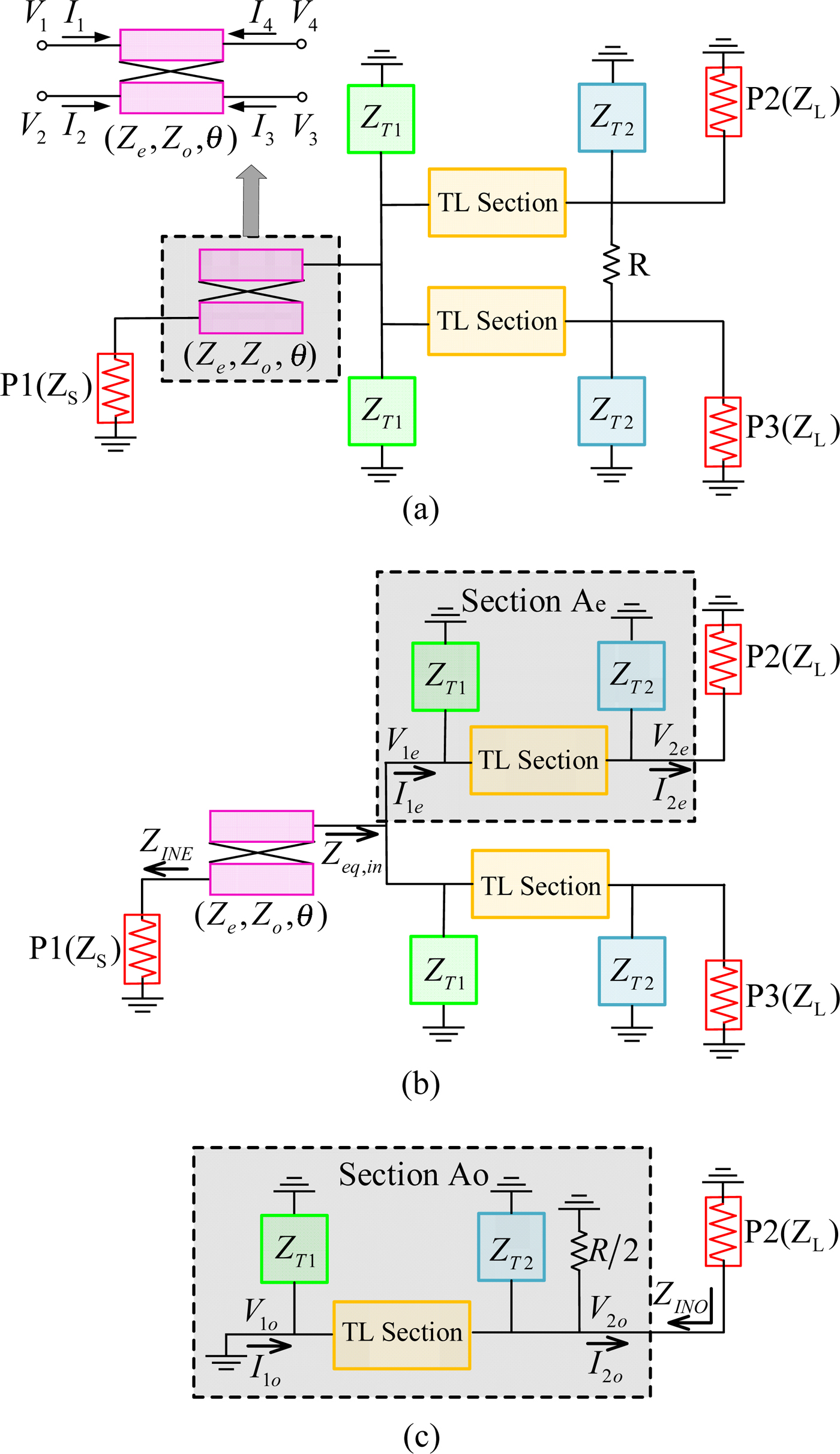
Fig. 1. Proposed WFPD circuit. (a) The schematic representation. (b) Even-mode equivalent circuit. (c) Odd-mode equivalent circuit.
As observed from Fig. 1(b), the terminal conditions of the four-port coupled lines can be expressed as equation (3). According to equation (3) and four-port impedance matrix of the coupled line shown in paper [Reference Tang, Tseng, Chiu and Wu20], the input impedance in port 1 (Z INE) can be calculated as equation (4). Thus, the reflection coefficient (S 11) and the transmission coefficient (S 21) can be extracted as equation (5).
 $$I_1 = I_3 = 0,$$
 $$V_4 = -Z_{eq,in}\cdot I_4,$$
 $$Z_{INE} = \displaystyle{{{(Z_e-Z_o)}^2{\csc} ^2\theta} \over {4Z_{eq,in}-{(Z_e + Z_o)}^2{\cot} ^2\theta}} -\displaystyle{{{(Z_e + Z_o)}^2{\cot} ^2\theta} \over 4},$$
 $$S_{11} = \left \vert {\displaystyle{{Z_{INE}-Z_S} \over {Z_{INE} + Z_S}}} \right \vert, $$
 $$S_{21} = \sqrt {1-{\left( {\displaystyle{{Z_{INE}-Z_S} \over {Z_{INE} + Z_S}}} \right)}^2}. $$
According to the odd-mode equivalent circuit shown in Fig. 1(c), the ABCD matrix of section A o could be expressed as equation (6), and input impedance in port 2 (Z INO) can be expressed as equation (7). Thus, the return loss in port 2 (S 22) could be deduced as equation (8).
 $$\left( {\matrix{ {A_{om}} & {B_{om}} \cr {C_{om}} & {D_{om}} \cr}} \right) = \left( {\matrix{ {A_{TL}} & {B_{TL}} \cr {C_{TL}} & {D_{TL}} \cr}} \right)\left( {\matrix{ 1 & 0 \cr {\displaystyle{1 \over {\,jX_{T2}}}} & 1 \cr}} \right)\left( {\matrix{ 1 & 0 \cr {\displaystyle{2 \over R}} & 1 \cr}} \right),$$
 $$Z_{INO} = \displaystyle{{Z_{2o}} \over {I_{2o}}} = \displaystyle{{B_{TL}} \over {A_{TL} + \displaystyle{{B_{TL}} \over {\,jX_{T2}}} + \displaystyle{{2B_{TL}} \over R}}},$$
 $$S_{22} = \left \vert {\displaystyle{{Z_{INO}-Z_L} \over {Z_{INO} + Z_L}}} \right \vert. $$
Two kinds of TL sections, i.e. (1) quarter-wavelength TL and (2) dual TLs (DTLs) are demonstrated in Fig. 2, which could be adopted to replace the TL section in the basic WFPD circuit. Three types of loading terminations, i.e. (3) short-circuited stub, (4) cascade open-circuited stub, and (5) short-circuited DTLs stub shown in Fig. 3 could be employed as the practical realization of Z T1 and Z T2. Various types of WFPDs can be designed with different TL sections and loading terminations.

Fig. 2. Two kinds of transmission line sections.

Fig. 3. Three kinds of loading terminations.
Analysis of specific WFPDs
In this section, the signals splitting and signals filtering performances of three different WFPDs are analyzed under even-mode excitation. Then, isolation performances are explained under odd-mode excitation.
Analysis of WFPD1 under even-mode excitation
For WFPD1, the loading termination Z T1 is selected as (3) short-circuited stub and the loading termination Z T2 is implemented as (4) cascade open-circuited stub, while TL section is chosen as (1) quarter-wavelength TL. Based on the schematic representation of WFPD1 shown in Table 1, ABCD parameters of the (1) quarter-wavelength transmission, X T1 and X T2 could be expressed as equation (9).
 $$\left( {\matrix{ {A_{TL}} & {B_{TL}} \cr {C_{TL}} & {D_{TL}} \cr}} \right) = \left( {\matrix{ {\cos \theta} & {\,jZ_1} \cr {\,jY_1} & {\cos \theta} \cr}} \right),$$
 $$X_{T1} = Z_2\tan \theta {\rm,} $$
 $$X_{T2} = \displaystyle{{Z_4\cot \theta ({\tan} ^2\theta -Z_3/Z_4)} \over {1 + Z_3/Z_4}},$$
 $$Z_{INE} = \displaystyle{{{(Z_e-Z_o)}^2Z_L} \over {2Z_1^2}}, $$
 $$f_{TZ0} = 0,$$
 $$f_{TZ1} = \displaystyle{{2f_0} \over \pi} \arctan \sqrt {Z_3/Z_4}, $$
 $$f_{TZ2} = 2f_0-\displaystyle{{2f_0} \over \pi} \arctan \sqrt {Z_3/Z_4}, $$
 $$f_{TZ3} = 2f_0.$$
Table 1. Summary of three WFPDs with different kinds of TL sections and loading terminations

At f 0, A TL = D TL = 1/X T1 = 1/X T2 = 0. Combining equations (4) and (9), the input impedance in port 1 (Z INE) could be calculated as equation (10) when WFPD1 is under even-mode excitation. According to equations (1–5) and (9), the expressions of TZs could be derived as equation (11), which agrees well with the normalized frequency response of WFPD1 demonstrated in Table 1. In the special case of Z S = Z L = 50 Ω, the initial values of Z e, Z o, and Z 1 can be calculated as 158, 60, and 69 Ω based on equation (10). The values of Z e, Z o, and Z 1are adjusted as 158, 60, and 63 Ω to obtain wider passband BW and equal ripple return loss response.
Analysis of WFPD2 under even-mode excitation
For WFPD2, the loading terminations Z T1and Z T2 are all implemented as (4) open-circuited stub, while the TL section is selected as (1) quarter-wavelength TL. The expressions of X T1 and X T2 can be deduced as equation (12) based on the schematic representation of WFPD2 demonstrated in Table 1.
 $$X_{T1} = \displaystyle{{Z_4{\kern 1pt} \cot \theta ({\tan} ^2\theta -Z_3/Z_4)} \over {1 + Z_3/Z_4}},$$
 $$X_{T2} = \displaystyle{{Z_6{\kern 1pt} \cot \theta ({\tan} ^2\theta -Z_5/Z_6)} \over {1 + Z_5/Z_6}},$$
 $$Z_{INE} = \displaystyle{{{(Z_e-Z_o)}^2Z_L} \over {2Z_1^2}}. $$
At center frequency f 0, A TL = D TL = 1/X T1 = 1/X T2 = 0. After substituting equations (9a) and (12) into (4), the input impedance in port 1 (Z INE) can be simplified as equation (13) when the WFPD2 is under even-mode excitation. In the special case of Z S = Z L = 50 Ω, the initial values of Z e, Z o, and Z 1 can be calculated as 158, 60, and 69 Ω based on equation (13). To realize wider passband BW and equal ripple return loss response, the values ofZ e, Z o, Z 1 are tuned as 158, 60, and 63 Ω, respectively.
Combining equations (1–5), (9a), and (12), the frequencies of the TZs below 2f 0 can be deduced as equation (14). It can be observed from the normalized frequency response that six TZs are introduced below 2f 0 in WFPD2, which agrees well with equation (14).
 $$f_{TZ0} = 0,$$
 $$f_{TZ1} = \displaystyle{{2f_0} \over \pi} {\kern 1pt} \arctan \sqrt {Z_3/Z_4}, $$
 $$f_{TZ2} = \displaystyle{{2f_0} \over \pi} {\kern 1pt} \arctan \sqrt {Z_5/Z_6}, $$
 $$f_{TZ3} = 2f_0-\displaystyle{{2f_0} \over \pi} {\kern 1pt} \arctan \sqrt {Z_5/Z_6}, $$
 $$f_{TZ4} = 2f_0-\displaystyle{{2f_0} \over \pi} {\kern 1pt} \arctan \sqrt {Z_3/Z_4}, $$
 $$f_{TZ5} = 2f_0.$$
Figure 4 shows the normalized frequency responses of WFPD2 with various values of Z3, Z4, Z 1, Z e, and Z o. As shown in Fig. 4(a), passband selectivity and passband BW are mainly influenced by the frequencies of f TZ1 and f TZ2, which can be adjusted by tuning the impedances of cascade open-circuited stubs (Z 3 and Z 4). The frequency of f TZ1 will shift to higher frequency and the frequency of f TZ2 will shift to lower frequency when the value of Z 3/Z 4increases, meanwhile the BW will become narrow when the value of Z 3/Z 4 increases. The conclusions came from Fig. 4(a) are in good agreement with equation (14). Apply the same principle to WFPD1, the required passband selectivity and BW could be realized by adjusting the value of Z 3/Z 4, which accords with equation (11).

Fig. 4. Normalized frequency responses of WFPD2 with various (a) Z 3 and Z 4, (b) Z 1, (c) Z e and Z o.
According to equations (10) and (13), the input impedance of port 1 (Z INE) in WFPD1 and WFPD2 is mainly affected by the values of Z 1, Z e, and Z o. Normalized frequency responses of WFPD2 with various values of Z 1, Z e, and Z o are shown in Figs 4(b) and 4(c), respectively. Figure 4(b) demonstrates that in-band return loss with constant BW can be optimized by selecting a proper value of Z 1. As observed in Fig. 4(c), the return loss in the passband frequency range is influenced by values of Z e and Z o. Thus, excellent in-band return loss in WFPD1 and WFPD2 could be realized by adjusting the values of Z 1, Z e, and Z o.
Analysis of WFPD3 under even-mode excitation
As for WFPD3, the loading termination Z T1 is implemented as (5) short-circuited DTLs and the loading termination Z T2 is chosen as (4) cascade open-circuited stub, while the TL section is selected as (2) DTLs. The ABCD matrix of the DTLs is demonstrated in equation (15a) which has been presented in paper [Reference Tang, Chen and Tsai21]. X T1 and X T2 can be expressed as equations (15b) and (15c).
 $$\left( {\matrix{ {\displaystyle{{\cos \alpha \sin \beta + \cos \beta \sin \alpha} \over {\sin \alpha + \sin \beta}}} & {\displaystyle{{\,jZ_S\sin \alpha \sin \beta} \over {\sin \alpha + \sin \beta}}} \cr {\,jY_S\displaystyle{{{(\cos \alpha -\cos \beta )}^2 + {(\sin \alpha + \sin \beta )}^2} \over {\sin \alpha + \sin \beta}}} & {\displaystyle{{\cos \alpha \sin \beta + \cos \beta \sin \alpha} \over {\sin \alpha + \sin \beta}}} \cr}} \right),$$
 $$X_{T1} = \displaystyle{{\tan \alpha + \tan \beta} \over {Z_5\tan \alpha \cdot \tan \beta}}, $$
 $$X_{T2} = \displaystyle{{Z_4\cot \theta ({\tan} ^2\theta -Z_3/Z_4)} \over {1 + Z_3/Z_4}}.$$
As shown in Fig. 2, the lengths of DTLs are defined as α, β, and α + β = 180°at f 0. Thus, A TL = D TL = 1/X T1 = 1/X T2 = 0 at f 0. According to equations (4) and (15), input impedance in port 1 (Z INE) could be calculated as equation (16) when WFPD3 is under even-mode excitation. In a special case of Z S = Z L = 50 Ω, the initial values of Z e, Z o, and Z 1 can be calculated as 150, 60, and 147 Ω based on equation (16). Moreover, the values of Z e, Z o, and Z 1 are adjusted as 150, 60, and 136 Ω to obtain wider BW and equal ripple return loss response. In WFPD3, the TZs below 2f 0 are expressed as equation (17) based on equations (1–5) and (15). The frequencies of TZs in series and parallel DTLs are shown in equation (18), which has been analyzed in our previous work [Reference Zhang, Wu, Yu and Liu22]. The normalized frequency response of WFPD3 is depicted in Table 1, which has a good agreement with equations (17 and 18).
 $$Z_{INE} = \displaystyle{{{(Z_e-Z_o)}^2({(\cos \alpha -\cos \beta )}^2 + {(\sin \alpha + \sin \beta )}^2)Z_L} \over {2Z_1^2 \sin \alpha \sin \beta}}, $$
 $$f_{TZ0} = 0,$$
 $$f_{TZ1} = \displaystyle{{2f_0} \over \pi} \arctan \sqrt {Z_3/Z_4}, $$
 $$f_{TZ2} = 2f_0-\displaystyle{{2f_0} \over \pi} \arctan \sqrt {Z_3/Z_4}, $$
 $$f_{TZ3} = 2f_0,$$
 $$f_{TZn}^S = \left\{ {\left. {(n + 1)f_0\left \vert {n\in N_ +, f \gt 0\left \vert {\tan \left( {\displaystyle{{\,f\alpha} \over {\,f_0}}} \right) = -\tan \left( {\displaystyle{{\,f\,(\pi -\alpha )} \over {\,f_0}}} \right)} \right.} \right.} \right\}} \right.,$$
 $$f_{TZn}^P = \left\{ {\left. {\displaystyle{{n\pi f_0} \over \alpha}, \displaystyle{{n\pi f_0} \over {(\pi -\alpha )}},n\in N_ +} \right\}} \right..$$
According to equation (16), the return loss of WFPD3 is mainly influenced by the values of Z e, Z o, and Z 1. It could be seen from equation (17) that the value of Z 3/Z 4 could be adjusted to obtain required BW and passband selectivity. Figure 5 shows the normalized frequency responses of WFPD3 with various electrical lengths (α). It could be observed from Fig. 5 that TZ could be obtained at 3f 0 when electrical length (α) is chosen as 60°, which accords to equation (18). The best out-of-band rejection performance could be obtained by defining the electrical length (α) as 60°.
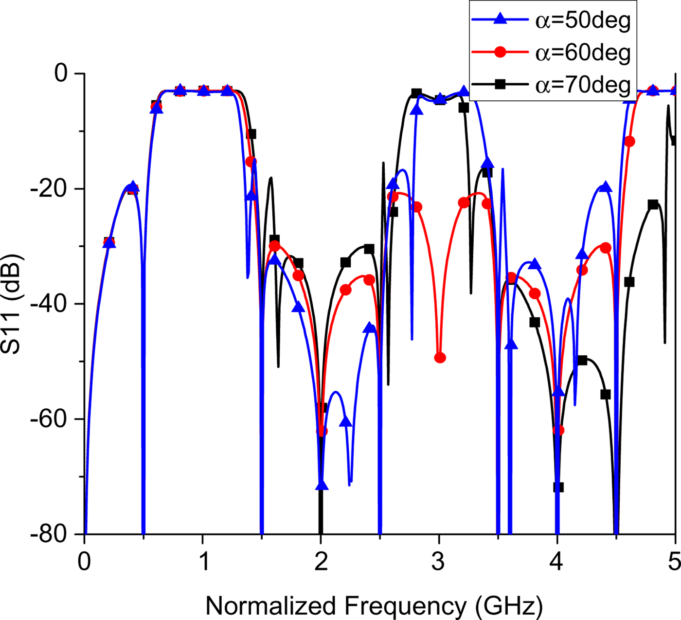
Fig. 5. Normalized frequency responses of WFPD3 with various electrical length (α).
Analysis of three WFPDs under odd-mode excitation
In WFPD1, WFPD2, and WPFD3, A TL = D TL = 1/X T1 = 1/X T2 = 0 at f 0. Under odd-mode excitation, the input impedance in port 2 (Z INO) could be simplified as R/2 based on equation (7).
Simulated and measured results
Discussion about S parameters
To verify the analysis above, the proposed three WFPDs have been constructed on the substrate with a relative dielectric constant of 3.5 and a thickness of 31 mil. The photographs and dimensions (unit: mm) of proposed WFPDs are shown in Table 1.
The EM-simulated and measured results of proposed WFPDs are shown in Figs 6–8. For WFPD1, the measured S 11 is >20 dB and the minimum insertion loss is 3.4 dB (including power division loss) in the passband, while the 3 dB fractional BW (FBW) is 79.7% from 1.81 to 4.21 GHz. As shown in Fig. 6(a), the measured harmonic suppression is >13.4 dB from 4.5 to 7.7 GHz. It is seen from Fig. 6(b) that measured S 22 is better than 11.6 dB during the operating band and the measured isolation (S 23) is higher than 13 dB from DC to 8 GHz.
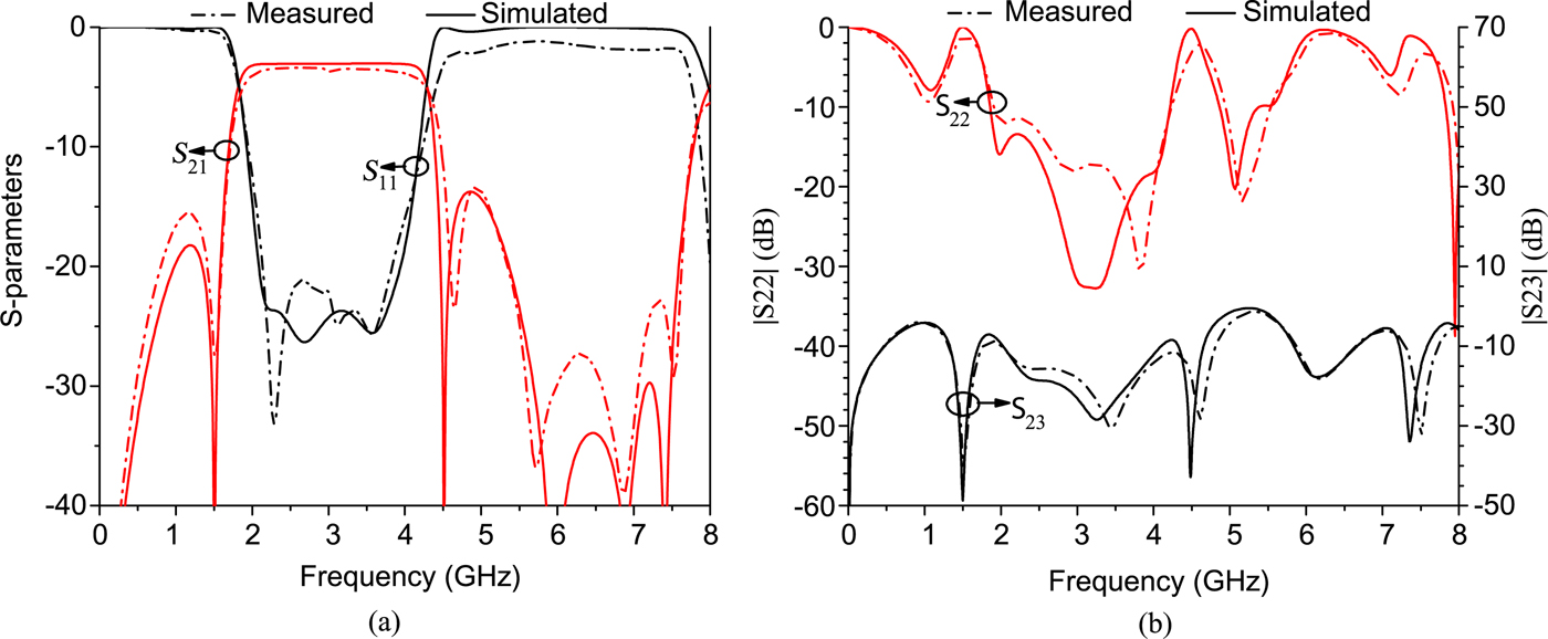
Fig. 6. Simulated and measured results of WFPD1. (a) S 11 and S 21, (b) S 22 and S 23.
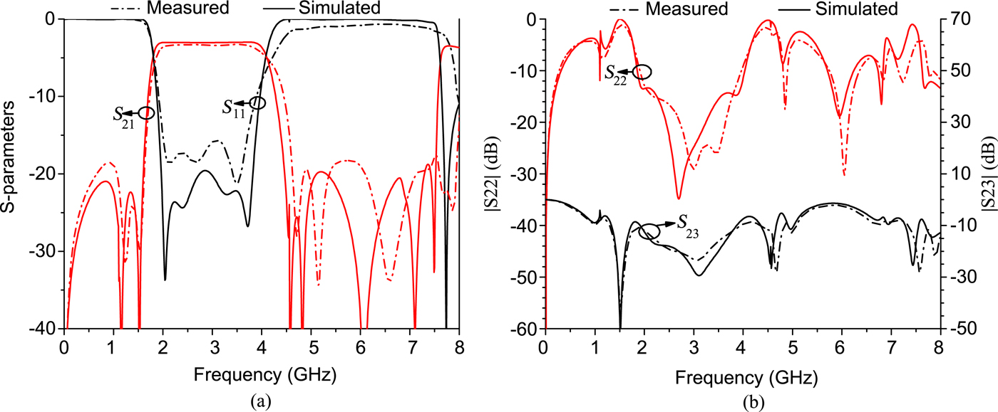
Fig. 7. Simulated and measured results of WFPD2. (a) S 11 and S 21, (b) S 22 and S 23.
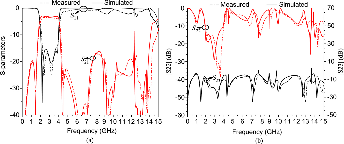
Fig. 8. Simulated and measured results of WFPD3. (a) S 11 and S 21, (b) S 22 and S 23.
For WFPD2, the measured S 11 is >15 dB and the minimum insertion loss is 3.3 dB (including power division loss) in the passband, while the 3 dB FBW is 79.0% from 1.80 to 4.15 GHz. As shown in Fig. 7(a), the measured harmonic suppression is >17.6 dB from 4.5 to 7.4 GHz. It is observed from Fig. 7(b) that measured S 22is better than 13 dB during the operating band and the measured isolation (S 23) is higher than 12 dB from DC to 8 GHz.
For WFPD3, the measured S 11 is >15 dB and the minimum insertion loss is 3.5 dB (including power division loss) in the passband, while the 3 dB FBW is 74.4% from 1.90 to 4.15 GHz. As shown in Fig. 8(a), the measured harmonic suppression is >17.0 dB from 4.5 to 14.25 GHz. It is observed from Fig. 8(b) that measured S 22 is better than 15.5 dB during the operating band and the measured isolation (S 23) is higher than 11.5 dB from DC to 15 GHz.
The comparisons between the proposed WFPDs and other published work are summaried in Table 2. Excellent performance including wide FBW, low insertion loss, wide upper stopband range with high attenuation and multiple TZs could be obtained in the proposed WFPDs.
Table 2. Comparisons between the proposed WFPDs and other published filtering PDs.

Discussion about power capacity
Coaxial lines and waveguides are usually employed to design microwave components with high power capacity, like high-power PDs [Reference Guo, Li, Huang, Shao and Ba23–Reference Guo, Li, Huang, Shao, Ba, Jiang, Jiang and Deng25]. Unlike the conventional Wilkinson PD with high power capacity, the proposed WFPD structures are mainly constructed by resonator-based impedance transforming networks which make their power capacity more similar to the resonator-based microstrip filters [Reference Endo, Ono, Uno, Satio, Satio, Nakajima and Ohshima26] as well as microstrip antennas [Reference Pozar27] with power capacity of several watts. However, the WFPDs in this paper are very attractive to design filtering microstrip antenna arrays or other microstrip transceiver circuits with low-power signals.
Conclusions
A series of WFPDs is proposed in this paper. Various kinds TL sections and loaded stubs are adopted to design different types of WFPDs. The proposed ideas are validated by the good agreement between simulated results and measured results of proposed WFPDs. The proposed three WFPDs have good filtering response and out-of-band rejection performances, which can fulfil the broadband communication requirements. Specifically, in this paper, WFPD1 is introduced with simple design process and compact circuit size to verify the proposed filtering PD structures and analysis. However, WFPD1 suffers from poor out-of-band rejection performance. By replacing short-circuited stubs in WFPD1 with cascade open-circuited stubs, WFPD2 is constructed with improved out-of-band rejection, but WFPD2 has the disadvantage of relative complicated design procedures and larger circuit size. Employing DTLs in WFPD3, the upper stopband frequency range is greatly extended. However, WFPD3 has the largest circuit size and most complicated design procedures. In the practical application, according to the requirements of circuit size, harmonic suppression performance as well as upper stopband BW, the sufficient WFPD type can be selected.
Acknowledgement
This work was supported in part by the National Natural Science Foundations of China (No. 61327806 and No. 61422103), in part by the National Basic Research Program of China (973 Program) under Grant 2014CB339900, and in part by 863 Program under Grant 2015AA016801.
 Gaoya Dong was born in Shanxi, China, in 1993. She received the B.S. degree in Applied Physics from Xidian University, Xi ’an, China, in 2015. She is currently pursuing the Ph.D. degree in Electrical Engineering in Beijing University of Posts and Telecommunications, Beijing, China. Her current research interests include planar microwave power dividers and antennas.
 Weimin Wang was born in Shandong, China, in 1977. She received the B.Eng. degree in Telecommunication Engineering, the M.Sc. degree in Electromagnetics and Microwave Technology, and the Ph.D. degree in Electronic and Information Engineering from the Beijing University of Posts and Telecommunications, Beijing, China, in 1999, 2004, and 2014, respectively.
 Bo Zhang was born in Shanxi, China, in 1991. He received the B.S. and M.S. degrees all in Electronic and Information Engineering from Beijing University of Posts and Telecommunications (BUPT), Beijing, China, in 2012 and 2015, respectively, where he is currently working toward Ph.D. degree in electrical engineering. His current research interests include planar microwave filters, power divider, antennas, and power amplifiers.
 Yuanan Liu received the B.E., M.Eng., and Ph.D. degrees in Electrical Engineering from the University of Electronic Science and Technology of China, Chengdu, China, in 1984, 1989, and 1992, respectively. In 1984, he joined the 26th institute of Electronic Ministry of China to develop the inertia navigating system. In 1992, he began his first post-doctor position in EMC laboratory of Beijing University of Posts and Telecommunications (BUPT), Beijing, China. In 1995, he started his second post-doctor in broadband mobile laboratory of Department of System and Computer Engineering, Carleton University, Ottawa, Canada. From July, 1997, as a professor, he is with wireless communication center of College of Telecommunication Engineering, BUPT, Beijing, China, where he is involved in the development of next-generation cellular system, wireless LAN, Bluetooth application for data transmission, EMC design strategies for high-speed digital system, and EMI and EMS measuring sites with low cost and high performance.


