


I. INTRODUCTION
Metallic nanostructured multilayered films (NMFs) exhibit excellent electrical, magnetic, and mechanical properties due to the presence of interfaces and a nanoscale layered structure. Reference Aydiner, Brown, Mara, Almer and Misra1–Reference Misra, Hirth and Hoagland6 NMFs are typically processed using various deposition methods including physical and chemical vapor deposition, as well as electrodeposition (ED). Among these, ED is a generally scalable and economical method, and it allows easy control of the composition and microstructure by adjusting deposition parameters such as current, potential, electrolyte composition, agitation etc. Reference Ross7 NMFs can be electrodeposited using either galvanostatic or potentiostatic control in a single or dual electrolyte bath. Reference Ross7,Reference Goldman, Ross, Ohashi, Wu and Spaepen8 In particular, galvanostatic control (current control) is advantageous in terms of tuning the layer thicknesses, especially at high current efficiencies where the deposited mass is directly related to the deposition time.
ED of Cu-, Ni-, and Fe-based NMFs has all been widely reported, whereas those containing light metals like Al and its alloys remain limited. Reference Stafford9,Reference Ali, Nishikata and Tsuru10 The difficulty lies in the fact that Al cannot be electrodeposited from aqueous solution, Reference Simka, Puszczyk and Nawrat11 so ED of Al and its alloys most frequently takes place in molten salts at elevated temperatures. Of increasing interest is ED from ionic liquids, which have made it possible to electrodeposit active metals and alloys from room temperature to ∼150 °C. Reference Simka, Puszczyk and Nawrat11–Reference Stafford and Hussey13 These ionic liquids, i.e., molten salts with a melting point below room temperature, contain substituted imidazolium or tetraalkylammonium organic cations and simple inorganic anions such as AlCl4¯, PF6¯, and BF4¯. Reference Simka, Puszczyk and Nawrat11 The asymmetric structure between the cation and anion leads to weak ionic bonding that significantly lowers the melting point. In addition, room temperature ionic liquids exhibit low vapor pressures even at temperatures up to 300 °C, high chemical and thermal stability, and most importantly wide electrochemical windows of more than 6 V. Reference Plieth14 Thus, it is possible to deposit less-noble metals and alloys including Al, Ti, Mo, Ta, etc. which generally cannot be deposited from aqueous solutions. Reference Endres15 The high purity of these electrolytes also permits extremely pure nanocrystalline metals to be deposited, thus avoiding common impurities such as sulfur and hydrogen which are commonly codeposited from aqueous solutions.
The present work builds on an earlier report, Reference Cai and Schuh16 in which we described ED of Al1−x Mn x /Al1−y Mn y (hereafter noted as Al–Mn) multilayers with a wide range of structures ranging from microcrystalline to nanocrystalline and amorphous, by tuning the electrolyte composition. In the present work we extend that study to 1) demonstrate the feasibility of ED of Al–Mn multilayers with both micrometer and nanometer layer thicknesses; 2) investigate the effect of deposition parameters on microstructure development and mechanical properties of these multilayers. We show that both grain size and its distribution can be tailored by carefully controlling the deposition conditions including the electrolyte composition, applied current density, and the current duration. The nanostructures and compositions of these alloys are characterized by analytical characterization tools including x-ray diffraction (XRD), scanning electron microscopy (SEM), and energy-dispersive spectroscopy (EDS). Grain morphologies, grain sizes, and the distribution of grain sizes are characterized by transmission electron microscopy (TEM) analysis. Finally, the mechanical properties of multilayered Al–Mn are investigated using nanoindentation and nanoscratch tests on selected samples.
II. EXPERIMENTAL PROCEDURE
Monolithic and multilayered Al–Mn samples were electrodeposited from room temperature ionic liquid electrolyte inside a nitrogen-filled glovebox with O2 and H2O levels maintained below 1 ppm. Prior to ED, the as-received 1-ethyl-3-methylimidazolium chloride (EMIC, 98%, IoLiTec) was dried under vacuum at 60 ° C for 3–5 days. The electrolyte is comprised of a 1:2 mole ratio of EMIC:AlCl3. This Lewis acidic solution with 66.7 m/o AlCl3–EMIC composition is chosen to ensure maximum solubility of MnCl2. Anhydrous MnCl2 (99.9%, Sigma-Aldrich) of 0.06–0.12 M was then added to the electrolyte and agitated for 24 h. A two electrode system is used for deposition where pure Cu (99.9%, online metals) and Al (99.99%, Sigma-Aldrich) plates were used as the cathode and anode respectively, at a separation distance of ∼2 cm. Both monolithic and multilayered Al–Mn samples were prepared using galvanostatic control. For the multilayered samples, the deposition current was alternated between 4 and 10 mA/cm2 using a pulsed current rectifier; the current level was fixed for two alternated durations called t 1 and t 2.
Al–Mn multilayers were analyzed using scanning electron microscope (SEM, Helios Nanolab 600, Hillsboro, OR) operated at 5 kV with calibrated energy-dispersive x-ray spectroscope (EDS, Oxford Instruments). X-ray diffraction (XRD, X'Pert PANalytical) was carried out using Cu Kα radiation at 45 kV and 40 mA. Transmission electron microscopy (TEM) analysis, selected area diffraction (SAD), and high angle annular dark-field (HAADF) imaging was performed using a JEOL 2010F instrument (Tokyo, Japan) operated at 200 kV. TEM samples were prepared by either a standard lift-out technique using FIB or conventional mechanical preparation followed by ion milling. Low current ion beams were used as the final step during FIB preparation to minimize Ga damage to the sample.
Nanoindentation tests were performed on polished cross-sections of samples at 10 mN load, 1 mN/s loading rate, using a Hysitron TriboIndenter with a Berkovich tip. The cross-sectioned samples were mechanically polished using various grades of SiC grit paper followed by silica suspensions with particle sizes down to 50 nm. Prior to nanoindentation tests, the tip area function was calibrated using a standard fused quartz sample. In all the nanoindentation tests reported here, the ratio between the final and maximum indentation depth, h f/h max is always smaller than 0.7, indicating negligible pile-up during indentation which allows the usage of the Oliver–Pharr method Reference Oliver and Pharr17 to extract hardness and modulus. Nanoscratch tests were performed on polished cross-sectioned samples using a 1 µm conical tip under 500 µN constant load at a scratch speed of 0.67 µm/s.
III. EFFECTS OF DEPOSITION PARAMETERS ON MONOLITHIC Al–Mn ALLOY COMPOSITION
Mn is nobler than Al in aqueous solution, but in the acidic chloroaluminate electrolyte, the deposition potential for Mn is slightly more negative than that for Al, Reference Verdieck and Yntema18 thus allowing Mn to be codeposited with Al. The overall reduction of Al–Mn occurs by the following reactions according to Refs. Reference Stafford and Hussey13,Reference Tremillo and Letisse19:
 $${\rm{M}}{{\rm{n}}^{2 + }} + 2{{\rm{e}}^ - } \leftrightarrow {\rm{Mn}}$$
and
 $$4{\rm{A}}{{\rm{l}}_2}{\rm{Cl}}_7^ - + 3{{\rm{e}}^ - } \leftrightarrow {\rm{Al}} + 7{\rm{AlCl}}_4^ - \quad {\rm{.}}$$
A. Effects of electrolyte composition
During codeposition of binary alloys, the alloy composition strongly depends on the electrolyte composition, which controls the concentration of electroactive species (Al2Cl7 − and Mn2+), as well as the deposition current/potential. To evaluate the effects of MnCl2 concentration in the electrolyte and the deposition current density (j) on the alloy composition, monolithic Al–Mn samples were first electrodeposited from electrolyte containing 0.03–0.12 M of MnCl2 at current densities of 4, 6, and 10 mA/cm2. The atomic fraction of Mn in the deposit, measured by EDX, together with data from a previous work by Ruan and Schuh, Reference Ruan and Schuh20 is shown in Fig. 1(a). It can be seen that at all current densities tested, alloy concentration increases with MnCl2 content, similar to those reported in Refs. Reference Stafford and Hussey13,Reference Uchida, Tsuda, Yamamoto, Seto, Abe and Shibuya21. The atomic fraction of Mn, M Mn, can be estimated from the compositions of the electroactive species in the electrolyte as Reference Stafford and Hussey13
 $${M_{{\rm{Mn}}}} = {1 \over {1 + 0.25{K^\prime }{{C_{{\rm{A}}{{\rm{l}}_2}{\rm{C}}l_7^ - }^*} \over {C_{{\rm{M}}{{\rm{n}}^{2 + }}}^*}}}}\quad {\rm{,}}$$
where ${C^*}$
is the molar fraction of the corresponding electroactive species, and
${C^*}$
is the molar fraction of the corresponding electroactive species, and $K^\prime = {\raise0.7ex\hbox{${k_{{\rm{Al}}} }$} \!\mathord{\left/ {\vphantom {{k_{{\rm{Al}}} } {k_{{\rm{Mn}}} }}}\right.\kern-\nulldelimiterspace}\!\lower0.7ex\hbox{${k_{{\rm{Mn}}} }$}}$
is the ratio of the first-order heterogeneous rate constant k
Al and k
Mn for the deposition reactions of Al and Mn, respectively.
$K^\prime = {\raise0.7ex\hbox{${k_{{\rm{Al}}} }$} \!\mathord{\left/ {\vphantom {{k_{{\rm{Al}}} } {k_{{\rm{Mn}}} }}}\right.\kern-\nulldelimiterspace}\!\lower0.7ex\hbox{${k_{{\rm{Mn}}} }$}}$
is the ratio of the first-order heterogeneous rate constant k
Al and k
Mn for the deposition reactions of Al and Mn, respectively. $C_{{\rm{M}}{{\rm{n}}^{2 + }}}^*$
is equal to the MnCl2 concentration in the electrolyte and
$C_{{\rm{M}}{{\rm{n}}^{2 + }}}^*$
is equal to the MnCl2 concentration in the electrolyte and $C_{{\rm{A}}{{\rm{l}}_2}{\rm{C}}l_7^ - }^*$
can be estimated from
Reference Boon, Levisky, Pflug and Wilkes22
$C_{{\rm{A}}{{\rm{l}}_2}{\rm{C}}l_7^ - }^*$
can be estimated from
Reference Boon, Levisky, Pflug and Wilkes22
 $$\left[ {{\rm{A}}{{\rm{l}}_2}{\rm{Cl}}_7^ - } \right] = {{\rho (2N - 1)} \over {\left( {1 - N} \right){M_{{\rm{EMIC}}}} + N{M_{{\rm{AlC}}{{\rm{l}}_3}}}}}\quad {\rm{,}}$$
where N is the molar fraction of AlCl3, M is the molecular weight, and ρ is the density of the electrolyte. For the current electrolyte system, N = 0.67, M
EMIC = 146.62 g/mol, ${M_{{\rm{AlC}}{{\rm{l}}_3}}} = 133.34\;{\rm{g}}/{\rm{mol}}$
, and ρ = 1.354 g/cm3. From Eq. (2), the calculated concentration
${M_{{\rm{AlC}}{{\rm{l}}_3}}} = 133.34\;{\rm{g}}/{\rm{mol}}$
, and ρ = 1.354 g/cm3. From Eq. (2), the calculated concentration $\left[ {{\rm{A}}{{\rm{l}}_2}{\rm{Cl}}_7^ - } \right]$
is 3.3 M,very close to that in the ratio 2:1 of AlCl3:NaCl inorganic chloroaluminate electrolyte system where
$\left[ {{\rm{A}}{{\rm{l}}_2}{\rm{Cl}}_7^ - } \right]$
is 3.3 M,very close to that in the ratio 2:1 of AlCl3:NaCl inorganic chloroaluminate electrolyte system where $\left[ {{\rm{A}}{{\rm{l}}_2}{\rm{Cl}}_7^ - } \right]$
is around 3.5 M.
Reference Stafford9
The expected alloy composition estimated from Eq. (1) is plotted as solid line in Fig. 1(a), with the best fit value
$\left[ {{\rm{A}}{{\rm{l}}_2}{\rm{Cl}}_7^ - } \right]$
is around 3.5 M.
Reference Stafford9
The expected alloy composition estimated from Eq. (1) is plotted as solid line in Fig. 1(a), with the best fit value ${K^\prime } \approx 1$
. The predicted composition agrees well with the experimental results, indicating that the reaction rates for Mn and Al deposition are indeed first order in their respective electroactive concentrations. The fact that
${K^\prime } \approx 1$
. The predicted composition agrees well with the experimental results, indicating that the reaction rates for Mn and Al deposition are indeed first order in their respective electroactive concentrations. The fact that ${K^\prime } \approx 1$
suggests that the rate constant dependence on the deposition current (or potential) is similar for reactions of both Al and Mn.
Reference Stafford and Hussey13
Some minor deviations are also observed, especially at high [MnCl2] and high current density, consistent with those observed in inorganic chloroaluminate electrolyte.
Reference Stafford9
It should also be pointed out that
${K^\prime } \approx 1$
suggests that the rate constant dependence on the deposition current (or potential) is similar for reactions of both Al and Mn.
Reference Stafford and Hussey13
Some minor deviations are also observed, especially at high [MnCl2] and high current density, consistent with those observed in inorganic chloroaluminate electrolyte.
Reference Stafford9
It should also be pointed out that $\left[ {{\rm{A}}{{\rm{l}}_2}{\rm{Cl}}_7^ - } \right]$
strongly depends on the acidity of the electrolyte; for the same system under Lewis base conditions (with N <0.5), the molar fraction of Al2Cl7
− is close to zero (<10−7 M).
Reference Boon, Levisky, Pflug and Wilkes22
Thus, maintaining a Lewis acid electrolyte is necessary for the ED of binary Al–Mn in the EMIC–AlCl3 system. This condition is however not necessary for Al–Mn deposition in inorganic chloroaluminate electrolyte systems such as NaCl–AlCl3, where the deposition can take place in basic solution involving the discharge of AlCl4
−.
Reference Li, Hjuler, Berg and Bjerrum23
$\left[ {{\rm{A}}{{\rm{l}}_2}{\rm{Cl}}_7^ - } \right]$
strongly depends on the acidity of the electrolyte; for the same system under Lewis base conditions (with N <0.5), the molar fraction of Al2Cl7
− is close to zero (<10−7 M).
Reference Boon, Levisky, Pflug and Wilkes22
Thus, maintaining a Lewis acid electrolyte is necessary for the ED of binary Al–Mn in the EMIC–AlCl3 system. This condition is however not necessary for Al–Mn deposition in inorganic chloroaluminate electrolyte systems such as NaCl–AlCl3, where the deposition can take place in basic solution involving the discharge of AlCl4
−.
Reference Li, Hjuler, Berg and Bjerrum23

FIG. 1. Mn concentration in monolithic Al–Mn alloy deposits as a function of (a) MnCl2 concentration in the electrolyte, and (b) deposition current density.
B. Effects of deposition current density
Whether and how the deposition current density (or potential) affects the Al–Mn alloy composition has been debated and contradictory results have been reported. For example, Uchida et al. Reference Uchida, Tsuda, Yamamoto, Seto, Abe and Shibuya21 found Al–Mn alloy composition was almost independent of current density/potential, while others Reference Stafford9,Reference Li, Nan and Jiang24–Reference Tsuda, Hussey and Stafford26 observed a strong dependence. Stafford Reference Stafford9 found Mn concentration increases with current density while the opposite was observed by Li Reference Li, Nan and Jiang24 and Grushko. Reference Grushko and Stafford25 Tsuda et al. Reference Tsuda, Hussey and Stafford26 showed that the Mn concentration increases with current density for j = 5–40 mA/cm2 and decreases with current density for j = 40–80 mA/cm2. Our results in Fig. 1(b) show that the Mn concentration in the alloy increases with deposition current density (i.e., with increasing cathodic overpotential) at [MnCl2] from 0.06 to 0.12 M, similar to that observed from inorganic chloroaluminate electrolyte. Reference Stafford9
When the MnCl2 concentration in the electrolyte is extremely low, reduction of Mn at all current densities is diffusion controlled. Thus, the Mn partial current remains constant while the Al partial current increases with increasing deposition current, resulting in a reduction of Mn concentration incorporated into the alloy, as seen by Grushko Reference Grushko and Stafford27 in electrolyte with 0.2 wt% (approximately 0.022 M) MnCl2. As the MnCl2 concentration increases, the addition of Mn2+ shifts the reduction potential of Al to more negative values due to a decrease in the Al ion activity, similarly to what is observed in the Al–Cr and Al–Ti systems. Reference Stafford9 Thus, higher [MnCl2] leads to a higher activation energy for deposition and the codeposition process changes from mass transfer limited to activation process dominated. This higher activation energy at high [MnCl2] also contributes to the formation of a finer microstructure and smoother surfaces, due to the promotion of lateral growth instead of growth of faceted nodules, as will be discussed in Sec. V. A. Tsuda et al. Reference Tsuda, Hussey and Stafford26 observed that when Mn content is above 0.07 M, the partial current for Mn deposition increases faster than Al with increasing current, since higher current (higher cathodic overpotential) favors the reduction of the less noble Mn. This result is also consistent with our observation in Fig. 1(b) where the effect of current density on alloy concentration is most significant at high MnCl2 concentration of [MnCl2] = 0.12 M, as compared to [MnCl2] = 0.06 and 0.09 M. When the deposition current is further increased toward the diffusion limit for both electroactive species, the alloy composition will depend only on the electrolyte composition and not on the applied current or potential, as observed by Stafford Reference Stafford9 from electrolytes containing 0.25–1.25 wt% (approximately 0.028–0.14 M) MnCl2 at potentials below −0.35 V/Al.
IV. Al–Mn MICROLAYERED FILMS
Results presented in Sec. III indicate that 1) the global Mn content in the alloy can be controlled by the MnCl2 concentration in the electrolyte; 2) the local Mn concentration in the alloy can be tailored by the deposition current below the diffusion limit. Taken together, it is thus possible to synthesize Al–Mn multilayers with alternating Mn-lean and Mn-rich layers by modulating the deposition current between a low and high value from a single electrolyte bath. To demonstrate the feasibility of synthesizing compositional modulating multilayers using one-bath galvanostatic control, we electrodeposited multilayered Al–Mn alloy by periodically alternating the deposition current density between j 1 = 10 and j 2 = 4 mA/cm2 with durations of t 1 = 50 min and t 2 = 2 h, respectively, in an electrolyte solution containing 0.1 M MnCl2 for a total of 9.3 h. These current durations are chosen to achieve equally spaced layers according to Faraday's law, assuming 100% current efficiency.
A. Microstructure of Al–Mn microlayered films
Figure 2(a) shows a cross-sectional SEM image of an Al–Mn microlayered film, where dense and uniform deposit with a total thickness of ∼60 µm can be seen. The bright (denoted as ‘A’) and dark (denoted as ‘B’) layers were deposited with current densities of 10 and 4 mA/cm2, respectively. The overlaid Al and Mn concentration profiles in Fig. 2(a) clearly indicate compositional modulation between Mn-lean and Mn-rich layers, with individual layer compositions as listed in Table I. As expected, layer A, deposited at higher current density (10 mA/cm2) exhibits a higher alloy concentration (11.1 at.% Mn) than layer B (9.8 at.% Mn).

FIG. 2. (a) Cross-sectional SEM image of Al–Mn microlayered film. Overlaid profiles in (a) are the Al and Mn concentration. (b) Friction coefficient and wear track depth profile measured from nanoscratch test on the cross-sectioned sample in (a).
TABLE I. Summary of layer thickness, composition, and mechanical properties of Al–Mn microlayered films.

For the sample in Fig. 2, the average individual layer thickness is 9.2 and 8.3 µm, and the corresponding average growth rate is 11.1 and 4.1 µm/h for layers A and B, respectively. A gradual decrease of ∼25% of layer thickness is observed from layer A1 to A3 (measurement for A4 is not included due to material loss at the edge during sample polishing), and B1 to B3. This thickness reduction is partly due to an increased surface roughness (thus increased surface area) as the film gets thicker. Measurement of surface roughness indicates ∼14% increase of the outmost surface area compared with the original area. Since the volume of material deposited in each layer remains constant under current control, this will lead to a decrease of layer thickness of ∼14%. Another possible contribution to the observed layer thickness reduction is decreased current efficiency at the lower effective current density that emerges as the surface roughens. Reference Li, Nan and Jiang24,Reference Li, Hjuler, Berg and Bjerrum28 The theoretical layer thickness estimated from Faraday's law is 12 µm, indicating a decrease of current efficiency from 88 to 66% for layer A and 81 to 58% for layer B.Nevertheless, it should be pointed out that despite the reduction in layer thickness, the compositions from layers A1 to A3 and B1 to B3 did not show significant variation.
B. Mechanical properties of Al–Mn microlayer films
Mechanical properties of the Al–Mn sample shown in Fig. 2 were examined by performing nanoindentation and nanoscratch tests on polished cross-sections. The results are summarized in Table I. As shown in Table I, layer A exhibits a hardness value of 4.3 GPa, ∼16% higher than layer B (3.7 GPa), indicating that the more highly alloyed layer is more resistant to plastic deformation. The elastic modulus of layer A is also slightly higher than B due to the higher stiffness of Mn than Al. Figure 2(b) shows the coefficient of friction and the wear track depth from a scratch test performed across a transition from layer B to A. A lower friction coefficient and smaller wear track depth is observed in layer A than layer B. The wear track widths (measured from SEM images) are 593 ± 15 and 643 ± 29 nm for layers A and B, respectively. The calculated wear rates (defined as total material volume loss divided by the scratching distance) of the two layers are shown in Table I; the higher wear resistance by greater than ∼40% in layer A is consistent with its ∼60% increased hardness relative to layer B. It is interesting to note that despite the small variation in composition (∼1.3 at.% Mn) between layers A and B, a quite noticeable difference in both mechanical and tribological properties is achieved in Al–Mn multilayers. This is because the nanostructure within a given layer is a strong function of composition, as seen in prior works on the same system, Reference Cai and Schuh16,Reference Ruan and Schuh20 and as explored in more detail in subsequent sections.
V. Al–Mn NANOLAMINATE
A. Microstructure of Al–Mn nanolaminate
Cross-sectional SEM images of nine Al–Mn nanolaminates electrodeposited from electrolytes with 0.06–0.12 M [MnCl2] are shown in Fig. 3. The composition and microstructure results are summarized in Table II. Reducing the current duration t 1 and t 2 leads to a reduced layer thickness. Typical composition variations of ∼1–3 at.% Mn are observed between the Mn-lean and Mn-rich layers, with more significant differentiation at high [MnCl2], similar to that observed from monolithic Al–Mn (see Fig. 1). SEM images of the respective sample surfaces are shown as insets in Fig. 3. Comparing samples with the same current duration at various electrolyte concentrations, it can be seen that surface morphology becomes smoother with increasing Mn content in the alloy; this is suggestive of the formation of finer microstructure (e.g., smaller grain size and/or greater content of amorphous phase). Note that for Mn-lean samples such as 1–3, each individual surface nodule may represent a single grain, whereas for Mn-rich samples such as 4–9, the nodules are most likely agglomerates of nanometer grains or even amorphous structure. Reference Ruan and Schuh29

FIG. 3. (a)-(i) Cross-sectional SEM images of nine Al-Mn nanolaminates (sample ID 1 to 9) electrodeposited using alternating current between 10 and 4 mA/cm2 for a total of 2 hrs. The insets show corresponding SEM images of the sample surfaces. All cross-sectioned samples are prepared by FIB with a protective Pt layer. Arrows indicate the thickness of two layers, or one wavelength.
TABLE II. Summary of composition, microstructure, and mechanical properties of nine Al–Mn nanolaminates. Mn concentrations of each layer are measured by EDX inside a TEM.

The grain morphology of multilayers grown under 0.06 M [Mn2+] is typical for those under kinetic control at small nucleation overpotential, where grain nucleation proceeds via Volmer–Weber island formation and the shapes of the grains are dictated by the surface energies of different facets. The following subsequent grain growth process, i.e., the formation of Mn-lean and Mn-rich layers then follows a layer-by-layer growth mechanism within the individual grain. In this case, when the cathodic current increases from 4 to 10 mA/cm2, the deposition rate increases (i.e., the atomic flux increases) without changing the overall growth mode. A transition of surface morphology from faceted grains to hemispherical nodules is observed when [Mn2+] content in the electrolyte is increased above 0.09 M, which indicates that the onset potential for deposition is shifted more negative from the equilibrium potential, leading to an increased energy barrier for island nucleation. This high nucleation overpotential leads to a high flux of adatoms on the surface, which then limits adatom surface diffusion thus forming hemispherical islands instead of well-defined facets.
Figure 4 shows the XRD results for the nine Al–Mn nanolaminates. Samples 1–3 exhibit a single fcc phase indicating the formation of supersaturated solid solutions; the Mn concentrations of 4.5–6.2 at.% in samples 1–3 are significantly higher than the equilibrium solubility of Mn in Al, which is <1 at.% around room temperature. For samples 4–6, significant peak broadening suggests the formation of nanocrystalline grains. In addition, a broad diffraction peak at 2θ ≈ 43° is also present, indicating the coexistence of amorphous structure (≈53% as determined from XRD peak area measurement). XRD results of samples 7–9 indicate the presence of a majority of amorphous phase (≈83%) with a small amount of fcc phase, as indicated by the low intensity (111) peak.

FIG. 4. XRD line scan of nine Al–Mn nanolaminates.
TEM analysis of samples 1–3 shows that the nanometer-scale compositional layers are much smaller than, and contained within, the much larger microcrystalline grains. Such structures are similar to conventional epitaxial multilayers, with the notable caveat that our compositional modulations are subtle concentration waves of Mn solute of only a few percent. An example is shown in Fig. 5 for sample 1. The bright-field TEM image in Fig. 5(a) shows the layered microstructure near a triple junction, which clearly indicates the continuous formation of compositional layers within individual grains. Figure 5(b) is a high-angle annular dark field (HAADF) image of sample 1 where the light and dark contrast corresponds to the Mn-rich (A) and Mn-lean (B) layers, respectively, confirmed by the EDS line scan in Fig. 5(c). The average composition of layers A and B is ∼6.2 and 4.5 at.% Mn, respectively, determined using nanobeam EDS analysis. Reducing the layer thickness from 124 to 42 nm for samples 1–3 leads to a decrease of average grain size from 7.3 to 2.6–3.5 µm, without affecting the composition of the individual layer nor the general form of the structure as a polycrystalline structure with compositional modulations within the individual grains.

FIG. 5. (a) Bright-field TEM image and (b) HAADF image of sample 1. (c) EDS line scan along arrow direction in (b).
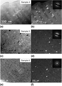
To reveal the detailed microstructure of samples 4–6, TEM analysis of cross-sectioned samples was performed as shown in Fig. 6. SAD patterns for all samples display both sharp diffraction rings and broad halos, indicating the coexistence of nanocrystalline and amorphous phase in these samples, consistent with the XRD results in Fig. 4. For all samples, the Mn-rich layers (A) have higher amorphous contents and smaller grain sizes as compared to the Mn-lean layers (B).

FIG. 6. (a, c, e) Bright field and (b, d, f) dark field cross-sectional TEM images of samples 4–6. Insets in (b, d, f) show the corresponding SAD patterns from multiple Mn-lean and Mn-rich layers.
Figure 7 shows the grain size distribution of samples 4–6, where decreasing the layer thickness (λ) leads to a decrease of the average grain size (d) for both layers. The mean grain sizes, obtained by fitting the grain size distribution using a normal distribution, are listed in Table II. The normal grain size distribution is perhaps suggestive of a diffusion-controlled grain roughening mechanism. Reference Carlson30 Another interesting observation is that for layer B, the upper bound of grain size (around 100, 70, and 50 nm for samples 4, 5, and 6, respectively) is very close to the corresponding layer thickness. This suggests that in at least some conditions, the layer thickness limits the growth of the grains, which nucleate fresh at each layer change. A practical consequence of this is that the grain size within the layers of an Al–Mn nanolaminate can be tailored by controlling the layer thickness; layering and interruptions of the deposition steady-state conditions can be used with the specific purpose of restricting the grain size. While the samples investigated here all consist of equally spaced layers, a larger grain size modulation between layers can be potentially achieved by increasing the layer thickness difference, which is left for future work.

FIG. 7. Grain size distribution of Mn-rich (A) and Mn-lean (B) layers for samples (a) 4, (b) 5, and (c) 6.
TEM analysis of samples 7–9 indicates that these materials contain a majority of amorphous phase with a small fraction of ultrafine grains of 3–5 nm. An example is shown in Fig. 8 for sample 7. The bright-field TEM image in Fig. 8(a) shows the composition modulation between the layers. SAD patterns taken from individual layers A and B in Fig. 8(a) and the corresponding intensity profile indicate a higher crystalline content in B. The average crystallite size, measured from high-resolution TEM, is about 3.2 and 5.2 nm for layers A and B, respectively. These nanocrystalline grains are equiaxed and often contain apparent defects. For example, the inset in Fig. 8(c) shows the formation of three small-angle subgrain boundaries, indicating the high level of packing frustration at high Mn concentrations.

FIG. 8. (a) Bright-field TEM image, and high-resolution TEM images of (b) layer A and (c) layer B of sample 7. Top left inset in (a) shows selected-area diffraction patterns from layers A and B. Top right inset in (a) shows the intensity profile along the arrows noted in the diffraction patterns.
Occasionally, nanometer scale icosahedral quasicrystalline particles (group symmetry $m\overline {35}$
) are also observed, as shown in Fig. 9. The inverse fast-Fourier transform pattern in Fig. 9 exhibits fifteen two-fold axes, which can be obtained by rotating 58.29° from a five-fold axis, similar to that shown by Shechtman et al. in fast quenched Al–Mn,
Reference Li, Nan and Jiang24
and also shown in the inset. Icosahedral quasicrystalline formation in the Al–Mn system has been observed in alloys with 10–14 at.% Mn after fast quenching or ED at elevated temperatures.
Reference Grushko and Stafford25
Recently, Ruan and Schuh
Reference Ruan and Schuh20
suggested that room temperature electrodeposited Al–15.8 at.% Mn contained nuclei of the icosahedral quasicrystalline phase. They reported an increase in the volume fraction of this phase after isothermal annealing at 310 °C, but they inferred that small, nanoscale nuclei must have been present in the as-deposited condition based on calorimetry data. The current work supports the idea that some nanoscale nuclei of icosahedral quasicrystalline phase are indeed present in Al–Mn electrodeposited at room temperature.
$m\overline {35}$
) are also observed, as shown in Fig. 9. The inverse fast-Fourier transform pattern in Fig. 9 exhibits fifteen two-fold axes, which can be obtained by rotating 58.29° from a five-fold axis, similar to that shown by Shechtman et al. in fast quenched Al–Mn,
Reference Li, Nan and Jiang24
and also shown in the inset. Icosahedral quasicrystalline formation in the Al–Mn system has been observed in alloys with 10–14 at.% Mn after fast quenching or ED at elevated temperatures.
Reference Grushko and Stafford25
Recently, Ruan and Schuh
Reference Ruan and Schuh20
suggested that room temperature electrodeposited Al–15.8 at.% Mn contained nuclei of the icosahedral quasicrystalline phase. They reported an increase in the volume fraction of this phase after isothermal annealing at 310 °C, but they inferred that small, nanoscale nuclei must have been present in the as-deposited condition based on calorimetry data. The current work supports the idea that some nanoscale nuclei of icosahedral quasicrystalline phase are indeed present in Al–Mn electrodeposited at room temperature.

FIG. 9. High-resolution TEM image of sample 7 demonstrating icosahedral phase formation. The top left inset is a fast Fourier transformation (FFT) taken from the whole image, revealing a symmetry with fifteen 2-fold axes, similar to the diffraction pattern along a 2-fold axis taken by Shechtman et al. PRL, 1984 (top central inset). An inverse fast Fourier transformation (IFFT) is calculated from the box area and shown in the lower right, along with a schematic image constructed from intersections of three icosahedra with the D3h symmetry.
To summarize, the above results indicate that the microstructure of multilayered Al–Mn nanolaminates is affected by the interplay between two structural length scales: grain size and layer thickness. When grain size is much larger than the layer thickness, as observed in samples 1–3 synthesized at 0.06 M [Mn2+], the composition modulation occurs within individual grains, similar to conventional epitaxial multilayers. In our case, the observed composition modulation was related to a change of Mn partial current as discussed in Sec. III. When layer thickness becomes comparable to the grain sizes, as observed in samples 4–9 synthesized at 0.09–0.12 M [Mn2+], composition modulation leads to the modulation of grain size as well as amorphous phase content between the layers. For samples 4–6, composition modulation between the Mn-rich and Mn-lean layers leads to a bimodal distribution of grain sizes. The layer-by-layer tuning of grain size seen in this system is unlike what is seen in conventional multilayer systems processed by other methods. According to the Scharifker–Hills model, Reference Scharifker and Hills31 grain nucleation during ED can be either instantaneous or progressive. In instantaneous nucleation, all nucleation sites are immediately activated and the rate of further nuclei formation is negligible, whereas progressive nucleation corresponds to continuous nuclei formation during the course of the deposition experiment. For samples 4–6, it is apparent that grain nucleation events take place progressively, leading to the formation of nanocrystalline grains of different sizes within each layer. The grains nucleated immediately at the layer interfaces broaden until they reach the next layer, resulting in a grain size close to the layer thickness. This grain growth mechanism is typical for polycrystalline thin film growth at low temperatures (grains become more columnar at higher temperature). Reference Dent, Seddon and Welton32
B. Mechanical properties of Al–Mn nanolaminates
Nanoindentation tests were performed on samples 1–9 and no difference was found between the hardnesses measured on the plane of the film or on cross-sectioned samples. Post-indentation SEM analysis shows a typical indentation width of ∼3 µm for all Al–Mn nanolaminates, which is much larger than the individual layer thicknesses. Thus, the measured hardness values are a good representation of the ‘composite hardness’ of the nanolaminates. Figure 10(b) shows the hardness as a function of layer thickness for the nine samples. A significant increase in hardness from ∼2.5 to 4.7 GPa is observed as the solution [MnCl2] concentration is increased from 0.06 to 0.12 M.

FIG. 10. Hardness as a function of layer thickness for samples 1–9.
Nanoscratch tests were performed on selected cross-sectioned samples over a scratch distance of 10 µm with the scratch direction parallel to the film growth direction. The average friction coefficients were 0.55, 0.54, and 0.45 for samples 1, 4, and 7 respectively, as listed in Table II, indicating multilayers that contain finer grains and higher Mn content exhibit better resistance to abrasive wear, consistent with their higher hardness values.
For multilayers where the layer thickness is smaller than the grain size, such as those deposited at 0.06 M [MnCl2] (i.e., samples 1–3), hardness increases as the layer thickness decreases. It should be pointed out that this hardness increment is different from those observed in conventional epitaxial multilayers with well-defined interfaces, where the strength is governed by confined dislocation movement across the interfaces. Reference Misra, Hirth and Hoagland6 In our case, only minor composition modulations are present across the layers, similar to those seen in dilute spinodally decomposed alloys. Reference Kato, Mori and Schwartz33,Reference Findik and Flower34 Kato and Schwartz Reference Kato, Mori and Schwartz33 showed that during spinodal hardening, the yield strength increases proportionally with the amplitude of composition modulation but independently of the wave length. Thus, the observed hardness increase in samples 2 and 3 is likely a result of their smaller grain sizes and higher defect density than sample 1, rather than a layer thickness effect. For multilayers where the grain size is comparable or smaller than layer thickness, such as those deposited at 0.09 and 0.12 M [MnCl2] (i.e., samples 4–7), hardness values are insensitive to the layer thickness. The average hardness agrees well with their corresponding rule of mixture hardness (H = V a H a + V b H b, where V i and H i represent the volume fraction and hardness of layer i), which is 3.9 and 4.6 GPa for samples 4–6 and 7–9, respectively (estimated from monolithic Al–Mn Reference Ruan and Schuh20 ).
VI. CONCLUSIONS
In summary, we demonstrate the ED of Al–Mn alloy multilayers from room temperature ionic liquid using galvanostatic control. Relatively subtle composition modulation between Mn-lean and Mn-rich layers leads to variations of both elastic and plastic properties within the multilayers. The microstructure of the multilayers can be tailored by ED parameters including electrolyte concentration, deposition current, and current duration. For multilayers where layer thickness is comparable to grain sizes, a bimodal grain size distribution is observed. The results of the current work thus provide a guideline for microstructure design of multilayers by controlling the deposition parameters.
ACKNOWLEDGMENTS
This work was supported by U.S. Army Research Office through the Institute for Soldier Nanotechnologies at MIT. The authors thankfully acknowledge the assistance of Dr. Alan Schwartzman for nanoindentation and nanoscratch testing, Dr. Shiyun Ruan for electrodeposition tests, Dr. Scott A Speakman for XRD measurement, and Dr. Yong Zhang for TEM analysis.


