Hostname: page-component-6b989bf9dc-476zt Total loading time: 0 Render date: 2024-04-14T07:56:47.345Z Has data issue: false hasContentIssue false

Nanostructured germanium prepared via ion beam modification

Published online by Cambridge University Press:  21 March 2013

Nicholas Guy Rudawski*
Affiliation:
Major Analytical Instrumentation Center, University of Florida, Gainesville, Florida 32611
Kevin Scott Jones
Affiliation:
Department of Materials Science and Engineering, University of Florida, Gainesville, Florida 32611
*
a)Address all correspondence to this author. e-mail: ngr@ufl.edu
Get access

Abstract

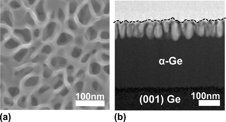
“Nanostructured” germanium (Ge; also known as “voided,” “porous,” “nanoporous,” “cratered,” and “honeycomb” Ge) created via ion beam modification has been studied for many years. This work reviews the progress made in studying and characterizing the nanostructured morphology, particularly via the use of experimental techniques such as scanning electron microscopy, atomic force microscopy, and transmission electron microscopy. Specifically, the empirical observations of the structural evolution of Ge as a function of ion beam modification conditions are discussed with added emphasis placed on quantification of the microstructure. The experimental observations and microstructure quantification are further discussed in terms of the implications for proposed formation mechanisms of the nanostructured morphology. Potential uses of the nanostructured morphology in chemical sensor and energy storage applications and suggested future lines of research to further the fundamental understanding of nanostructuring in Ge using ion beam modification are also presented.

Type
Reviews
Copyright
Copyright © Materials Research Society 2013 

Access options

Get access to the full version of this content by using one of the access options below. (Log in options will check for institutional or personal access. Content may require purchase if you do not have access.)

References

REFERENCES

Gleiter, H.: Nanostructured materials: Basic concepts and microstructure. Acta Mater. 48, 129 (2000).CrossRefGoogle Scholar
Arico, A.S., Bruce, P., Scrosati, B., Tarascon, J.M., and Van Schalkwijk, W.: Nanostructured materials for advanced energy conversion and storage devices. Nat. Mater. 4, 366377 (2005).CrossRefGoogle ScholarPubMed
Kang, B. and Ceder, G.: Battery materials for ultrafast charging and discharging. Nature 458, 190193 (2009).CrossRefGoogle ScholarPubMed
Simon, P. and Gogotsi, Y.: Materials for electrochemical capacitors. Nat. Mater. 7, 845854 (2008).CrossRefGoogle ScholarPubMed
Bruce, P.G., Scrosati, B., and Tarascon, J.M.: Nanomaterials for rechargeable lithium batteries. Angew. Chem. Int. Ed. 47, 29302946 (2008).CrossRefGoogle ScholarPubMed
Dresselhaus, M.S., Chen, G., Tang, M.Y., Yang, R., Lee, H., Wang, D., Ren, Z., Fleurial, J-P., and Gogna, P.: New directions for low-dimensional thermoelectric materials. Adv. Mater. 19, 10431053 (2007).CrossRefGoogle Scholar
Gratzel, M.: Mesoporous oxide junctions and nanostructured solar cells. Curr. Opin. Colloid Interface Sci. 4, 314321 (1999).CrossRefGoogle Scholar
Huang, X-J. and Choi, Y-K.: Chemical sensors based on nanostructured materials. Sens. Actuators, B 122, 659671 (2007).CrossRefGoogle Scholar
Li, W.Y., Xu, L.N., and Chen, J.: Co3O4 nanomaterials in lithium-ion batteries and gas sensors. Adv. Funct. Mater. 15, 851857 (2005).CrossRefGoogle Scholar
Yu, A.M., Liang, Z.J., Cho, J., and Caruso, F.: Nanostructured electrochemical sensor based on dense gold nanoparticle films. Nano Lett. 3, 12031207 (2003).CrossRefGoogle Scholar
Konstantatos, G. and Sargent, E.H.: Nanostructured materials for photon detection. Nat. Nanotech. 5, 391400 (2010).CrossRefGoogle ScholarPubMed
LaVan, D.A., McGuire, T., and Langer, R.: Small-scale systems for in vivo drug delivery. Nat. Biotech. 21, 11841191 (2003).CrossRefGoogle ScholarPubMed
Wang, Y.M., Chen, M.W., Zhou, F.H., and Ma, E.: High tensile ductility in a nanostructured metal. Nature 419, 912915 (2002).CrossRefGoogle Scholar
Choi, J.W., McDonough, J., Jeong, S., Yoo, J.S., Chan, C.K., and Cui, Y.: Stepwise nanopore evolution in one-dimensional nanostructures. Nano Lett. 10, 14091413 (2010).CrossRefGoogle ScholarPubMed
Destefanis, G.L. and Gailliard, J.P.: Very efficient void formation in ion-implanted InSb. Appl. Phys. Lett. 36, 4042 (1980).CrossRefGoogle Scholar
Kleitman, D. and Yearian, H.J.: Radiation-induced expansion of semiconductors. Phys. Rev. 108, 901 (1957).CrossRefGoogle Scholar
Nitta, N., Taniwaki, M., Hayashi, Y., and Yoshiie, T.: Formation of cellular defect structure on GaSb ion-implanted at low temperature. J. Appl. Phys. 92, 17991802 (2002).CrossRefGoogle Scholar
Perez-Bergquist, A., Zhu, S., Sun, K., Xiang, X., Zhang, Y., and Wang, L.M.: Embedded nanofibers induced by high-energy ion irradiation of bulk GaSb. Small 4, 11191124 (2008).CrossRefGoogle ScholarPubMed
Shaanan, M., Kalish, R., and Richter, V.: Changes in InSb as a result of ion implantation. Nucl. Instrum. Methods Phys. Res., Sect. B 78, 443447 (1985).CrossRefGoogle Scholar
Appleton, B.R., Holland, O.W., Narayan, J., Schow, O.E., Williams, J.S., Short, K.T., and Lawson, E.: Characterization of damage in ion implanted Ge. Appl. Phys. Lett. 41, 711712 (1982).CrossRefGoogle Scholar
Wilson, I.H.: The effects of self-ion bombardment (30-500 keV) on the surface topography of single-crystal germanium. J. Appl. Phys. 53, 16981705 (1982).CrossRefGoogle Scholar
Holland, O.W., Appleton, B.R., and Narayan, J.: Ion implantation damage and annealing in germanium. J. Appl. Phys. 54, 22952301 (1983).CrossRefGoogle Scholar
Lawson, E.M., Short, K.T., Williams, J.S., Appleton, B.R., Holland, O.W., and Schow, O.E.: Anomalous near-surface effects in room temperature implanted germanium. Nucl. Instrum. Methods Phys. Res. 209, 303307 (1983).CrossRefGoogle Scholar
Romano, L., Impellizzeri, G., Tomasello, M.V., Giannazzo, F., Spinella, C., and Grimaldi, M.G.: Nanostructuring in Ge by self-ion implantation. J. Appl. Phys. 107, 084314 (2010).CrossRefGoogle Scholar
Darby, B.L., Yates, B.R., Rudawski, N.G., Jones, K.S., Kontos, A., and Elliman, R.G.: Insights for void formation in ion-implanted Ge. Thin Solid Films 519, 59625965 (2011).CrossRefGoogle Scholar
Kaiser, R.J., Koffel, S., Pichler, P., Bauer, A.J., Amon, B., Claverie, A., Benassayag, G., Scheiblin, P., Frey, L., and Ryssel, H.: Honeycomb voids due to ion implantation in germanium. Thin Solid Films 518, 23232325 (2010).CrossRefGoogle Scholar
Stritzker, B., Elliman, R.G., and Zou, J.: Self-ion-induced swelling of germanium. Nucl. Instrum. Methods Phys. Res., Sect. B 175, 193196 (2001).CrossRefGoogle Scholar
Romano, L., Impellizzeri, G., Bosco, L., Ruffino, F., Miritello, M., and Grimaldi, M.G.: Nanoporosity induced by ion implantation in deposited amorphous Ge thin films. J. Appl. Phys. 111, 113515 (2012).CrossRefGoogle Scholar
Glover, C.J., Ridgway, M.C., Byrne, A.P., Yu, K.M., Foran, G.J., Clerc, C., Hansen, J.L., and Larsen, A.N.: Micro- and macro-structure of implantation-induced disorder in Ge. Nucl. Instrum. Methods Phys. Res., Sect. B 161, 10331037 (2000).CrossRefGoogle Scholar
Ridgway, M.C., Glover, C.J., Yu, K.M., Foran, G.J., Clerc, C., Hansen, J.L., and Larsen, A.N.: Ion-dose-dependent microstructure in amorphous Ge. Phys. Rev. B 61, 1258612589 (2000).CrossRefGoogle Scholar
Yates, B.R., Darby, B.L., Elliman, R.G., and Jones, K.S.: Role of nucleation sites on the formation of nanoporous Ge. Appl. Phys. Lett. 101, 131907 (2012).CrossRefGoogle Scholar
Chen, Y.J., Wilson, I.H., Cheung, W.Y., Xu, J.B., and Wong, S.P.: Ion implanted nanostructures on Ge(111) surfaces observed by atomic force microscopy. J. Vac. Sci. Technol., B 15, 809813 (1997).CrossRefGoogle Scholar
Huber, H., Assmann, W., Karamian, S.A., Mucklich, A., Prusseit, W., Gazis, E., Grotzschel, R., Kokkoris, M., Kossionidis, E., Mieskes, H.D., and Vlastou, R.: Void formation in Ge induced by high energy heavy ion irradiation. Nucl. Instrum. Methods Phys. Res., Sect. B 122, 542546 (1997).CrossRefGoogle Scholar
Ottaviano, L., Verna, A., Grossi, V., Parisse, P., Piperno, S., Passacantando, M., Impellizzeri, G., and Priolo, F.: Surface morphology of Mn+ implanted Ge (100): A systematic investigation as a function of the implantation substrate temperature. Surf. Sci. 601, 26232627 (2007).CrossRefGoogle Scholar
Kogler, R., Mucklich, A., Skorupa, W., Peeva, A., Kuznetsov, A.Y., Christensen, J.S., and Svensson, B.G.: Excess vacancies in high energy ion implanted SiGe. J. Appl. Phys. 101, 033508 (2007).CrossRefGoogle Scholar
Bellon, P., Chey, S.J., Vannostrand, J.E., Ghaly, M., Cahill, D.G., and Averback, R.S.: Surface damage produced by 20 keV Ga bombardment of Ge (001). Surf. Sci. 339, 135141 (1995).CrossRefGoogle Scholar
Gaertner, K., Joehrens, J., Steinbach, T., Schnohr, C.S., Ridgway, M.C., and Wesch, W.: Void formation in amorphous germanium due to high electronic energy deposition. Phys. Rev. B 83, 224106 (2011).CrossRefGoogle Scholar
Ghaly, M., Nordlund, K., and Averback, R.S.: Molecular dynamics investigations of surface damage produced by kiloelectronvolt self-bombardment of solids. Philos. Mag. A 79, 795820 (1999).CrossRefGoogle Scholar
Mayr, S.G. and Averback, R.S.: Ion-irradiation-induced stresses and swelling in amorphous Ge thin films. Phys. Rev. B 71, 134102 (2005).CrossRefGoogle Scholar
Claeys, C., Simoen, E., Opsomer, K., Brunco, D.P., and Meuris, M.: Defect engineering aspects of advanced Ge process modules. Mater. Sci. Eng., B 154, 4955 (2008).CrossRefGoogle Scholar
Claverie, A., Koffel, S., Cherkashin, N., Benassayag, G., and Scheiblin, P.: Amorphization, recrystallization and end of range defects in germanium. Thin Solid Films 518, 23072313 (2010).CrossRefGoogle Scholar
Koffel, S., Cherkashin, N., Houdellier, F., Hytch, M.J., Benassayag, G., Scheiblin, P., and Claverie, A.: End of range defects in Ge. J. Appl. Phys. 105, 126110 (2009).CrossRefGoogle Scholar
Koffel, S., Scheiblin, P., Claverie, A., and Benassayag, G.: Amorphization kinetics of germanium during ion implantation. J. Appl. Phys. 105, 013528 (2009).CrossRefGoogle Scholar
Birtcher, R.C.: Energy-dependent amorphization of Ge by Ne, Ar or Kr ion irradiation. Philos. Mag. B 73, 677688 (1996).CrossRefGoogle Scholar
Rudawski, N.G., Yates, B.R., Holzworth, M.R., Jones, K.S., Elliman, R.G., and Volinsky, A.A.: Ion beam-mixed Ge electrodes for high capacity Li rechargeable batteries. J. Power Sources 223, 336340 (2013).CrossRefGoogle Scholar
Rudawski, N.G., Darby, B.L., Yates, B.R., Jones, K.S., Elliman, R.G., and Volinsky, A.A.: Nanostructured ion beam-modified Ge films for high capacity Li ion battery anodes. Appl. Phys. Lett. 100, 083111 (2012).CrossRefGoogle Scholar
Ziegler, J.F.: SRIM-2003. Nucl. Instrum. Methods Phys. Res., Sect. B 219, 10271036 (2004).CrossRefGoogle Scholar
Prins, J.F., Derry, T.E., and Sellschop, J.P.F.: Volume expansion of diamond during ion-implantation. Phys. Rev. B 34, 88708874 (1986).CrossRefGoogle ScholarPubMed
Steinbach, T., Wernecke, J., Kluth, P., Ridgway, M.C., and Wesch, W.: Structural modifications of low-energy heavy-ion irradiated germanium. Phys. Rev. B 84, 104108 (2011).CrossRefGoogle Scholar
Janssens, T., Huyghebaert, C., Vanhaeren, D., Winderickx, G., Satta, A., Meuris, M., and Vandervorst, W.: Heavy ion implantation in Ge: Dramatic radiation induced morphology in Ge. J. Vac. Sci. Technol., B 24, 510514 (2006).CrossRefGoogle Scholar
Kim, J.C., Cahill, D.G., and Averback, R.S.: Formation and annihilation of nanocavities during keV ion irradiation of Ge. Phys. Rev. B 68, 094109 (2003).CrossRefGoogle Scholar
Kim, J.C., Cahill, D.G., and Averback, R.S.: Surface defects created by 20 keV Xe ion irradiation of Ge(111). Surf. Sci. 574, 175180 (2005).CrossRefGoogle Scholar
Peto, G., Horvath, Z.F., Gereben, O., Pusztai, L., Hajdu, F., and Svab, E.: Implantation-induced structural changes in evaporated amorphous Ge. Phys. Rev. B 50, 539542 (1994).CrossRefGoogle ScholarPubMed
Impellizzeri, G., Romano, L., Bosco, L., Spinella, C., and Grimaldi, M.G.: Nanoporosity induced by ion implantation in germanium thin films grown by molecular beam epitaxy. Appl. Phys. Express 5, (2012).CrossRefGoogle Scholar
Steinbach, T., Schnohr, C.S., Kluth, P., Giulian, R., Araujo, L.L., Sprouster, D.J., Ridgway, M.C., and Wesch, W.: Influence of electronic energy deposition on the structural modification of swift heavy-ion-irradiated amorphous germanium layers. Phys. Rev. B 83, (2011).CrossRefGoogle Scholar
Wesch, W., Schnohr, C.S., Kluth, P., Hussain, Z.S., Araujo, L.L., Giulian, R., Sprouster, D.J., Byrne, A.P., and Ridgway, M.C.: Structural modification of swift heavy ion irradiated amorphous Ge layers. J. Phys. D 42, (2009).CrossRefGoogle Scholar
Roorda, S., Sinke, W.C., Poate, J.M., Jacobson, D.C., Dierker, S., Dennis, B.S., Eaglesham, D.J., Spaepen, F., and Fuoss, P.: Structural relaxation and defect annihilation in pure amorphous silicon. Phys. Rev. B 44, 37023725 (1991).CrossRefGoogle ScholarPubMed
Vandenhoven, G.N., Liang, Z.N., Niesen, L., and Custer, J.S.: Evidence for vacancies in amorphous silicon. Phys. Rev. Lett. 68, 37143717 (1992).CrossRefGoogle Scholar
Lim, D.R., Rafferty, C.S., and Klemens, F.P.: The role of the surface in transient enhanced diffusion. Appl. Phys. Lett. 67, 23022304 (1995).CrossRefGoogle Scholar
Impellizzeri, G., Romano, L., Fraboni, B., Scavetta, E., Ruffino, F., Bongiorno, C., Privitera, V., and Grimaldi, M.G.: Nanoporous Ge electrode as a template for nano-sized (<5 nm) Au aggregates. Nanotechnology 23, (2012).CrossRefGoogle ScholarPubMed
Wohltjen, H. and Snow, A.W.: Colloidal metal-insulator-metal ensemble chemiresistor sensor. Anal. Chem. 70, 28562859 (1998).CrossRefGoogle Scholar
Sangster, J. and Pelton, A.: The Ge-Li (germanium-lithium) system. J. Phase Equilib. 18, 289294 (1997).CrossRefGoogle Scholar
Fuller, C.S. and Severiens, J.C.: Mobility of impurity ions in germanium and silicon. Phys. Rev. 96, 2124 (1954).CrossRefGoogle Scholar
Huggins, R. and Nix, W.: Decrepitation model for capacity loss during cycling of alloys in rechargeable electrochemical systems. Ionics 6, 5763 (2000).CrossRefGoogle Scholar
Davidson, S.M. and Booker, G.R.: Damage produced by ion implantation in silicon. Radiat. Effects 6, 3343 (1970).CrossRefGoogle Scholar
Davies, J.A., Denharto, J., Eriksson, L., and Mayer, J.W.: Ion implantation of silicon. I. atom location and lattice disorder by means of 1.0-MeV helium ion scattering. Can. J. Phys. 45, 40534071 (1967).CrossRefGoogle Scholar
Morehead, F.F. and Crowder, B.L.: A model for the formation of amorphous Si by ion bombardment. Radiat. Effects 6, 2732 (1970).CrossRefGoogle Scholar