Hostname: page-component-76fb5796d-25wd4 Total loading time: 0 Render date: 2024-04-25T09:29:22.096Z Has data issue: false hasContentIssue false

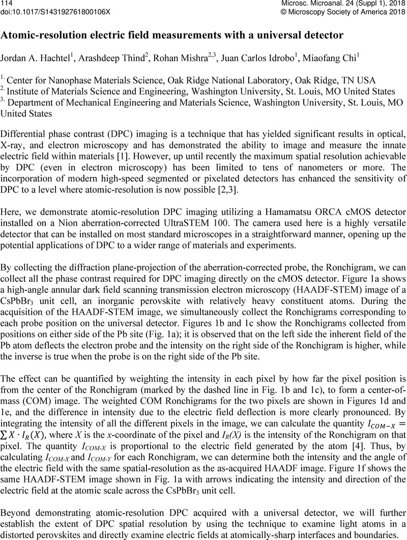
Atomic-resolution electric field measurements with a universal detector

Published online by Cambridge University Press:  01 August 2018

Jordan A. Hachtel
Affiliation:
Center for Nanophase Materials Science, Oak Ridge National Laboratory, Oak Ridge, TN USA
Arashdeep Thind
Affiliation:
Institute of Materials Science and Engineering, Washington University, St. Louis, MO United States
Rohan Mishra
Affiliation:
Institute of Materials Science and Engineering, Washington University, St. Louis, MO United States Department of Mechanical Engineering and Materials Science, Washington University, St. Louis, MO United States
Juan Carlos Idrobo
Affiliation:
Center for Nanophase Materials Science, Oak Ridge National Laboratory, Oak Ridge, TN USA
Miaofang Chi
Affiliation:
Center for Nanophase Materials Science, Oak Ridge National Laboratory, Oak Ridge, TN USA

Abstract

Image of the first page of this content. For PDF version, please use the ‘Save PDF’ preceeding this image.'
Type
Abstract
Copyright
© Microscopy Society of America 2018 

References

[1] Dekkers, N.H. de Lang, H. Optik. 41 1974) p 452.Google Scholar
[2] Shibata, N., et al., Nat. Phys. 8 2012) p 611.Google Scholar
[3] Yang, H., et al., Nat. Comm. 7 2016 ncomms12532.Google Scholar
[4] Close, R., et al., Ultramicroscopy 159 2015) p 124.Google Scholar
[5] Research supported by ORNL's Center for Nanophase Materials Sciences, which is a U.S. Department of Energy Office of Science User Facility.Google Scholar