Introduction
The ability to characterize emission processes at the nanoscale is critically important to the understanding of carrier trapping and recombination processes within nanoscale features such as defects and quantum disks (QDisks) within individual nanowires. Electron energy-loss spectroscopy (EELS) performed in the scanning transmission electron microscope (STEM) can potentially provide high spatial resolution but in most instruments the energy resolution is insufficient to differentiate small energy band differences. Furthermore, EELS probes the excitation rather than the emission process, making a direct comparison with well-established methods such as photoluminescence spectroscopy challenging. Cathodoluminescence (CL) spectroscopy is commonly used in the scanning electron microscope (SEM) for semiconductor studies, but the SEM lacks the spatial resolution to resolve quantum confined structures (Pennycook & Howie, Reference Pennycook and Howie1980; Garayt et al., Reference Garayt, Gérard, Enjalbert, Ferlazzo, Founta, Martinez-Guerrero, Rol, Araujo, Cox, Daudin, Gayral, Si Dang and Mariette2005; Strunk et al., Reference Strunk, Albrecht and Scheel2006; Yamamoto et al., Reference Yamamoto, Bhunia and Watanabe2006). While CL has been performed in the TEM/STEM for a number of years (see e.g., Roberts & Steeds, Reference Roberts and Steeds1982), it has been hampered by poor signal-to-noise ratios (SNRs) in the recorded spectra, which limited the use of the technique. Recent advances in detector technology have improved this situation considerably, opening the intriguing possibility of performing spatially resolved CL in the STEM with high SNR, potentially with simultaneous EELS measurements. STEM-CL should enable site-selective generation of electron-hole pairs at precise locations within engineered nano-heterostructures. As the excited electrons and holes relax, they undergo drift and diffusion processes that directly depend on the details of the local potential landscape. CL spectroscopy information correlated with the high-resolution imaging signal in the STEM could be a very powerful method for probing electron and hole behavior in nano-engineered structures.
An area where such characterization would prove particularly insightful is group-III nitride-based nanowires which have attracted attention for their potential in solid-state light emitter applications (Ponce & Bour, Reference Ponce and Bour1997; Kim et al., Reference Kim, Cho, Lee, Kim, Ryu, Kim, Kang and Chung2004; Qian et al., Reference Qian, Li, Gradečak, Wang, Barrelet and Lieber2004). QDisks within these nanowires represent ideal active regions due to their superior tunability as a result of strain tolerance and lack of extended defects (Miller et al., Reference Miller, Chemla, Damen, Gossard, Wiegmann, Wood and Burrus1984; Cho et al., Reference Cho, Kwon, Barjon, Brault, Daudin, Mariette and Dang2003; Renard et al., Reference Renard, Songmuang, Tourbot, Bougerol, Daudin and Gayral2009), exhibiting internal quantum efficiencies of up to 80% in AlGaN nanowires (Zhao et al., Reference Zhao, Djavid and Mi2015) and up to 62% in InGaN nanowires (Cui et al., Reference Cui, Fathololoumi, Golam Kibria, Botton and Mi2012). Despite their fundamental potential, nanowire light-emitting diode (LEDs) based on these QDisk active regions, with overall efficiencies <0.1%, have yet to compete with established thin film based LEDs with visible wavelength efficiencies >50%. Prior work has shown that most individual nanowires within a nanowire ensemble do not emit electroluminescence (EL), which has lower spectral resolution than CL, but should provide the same spectral features, suggesting that one major contributor to these low efficiencies lies in the difficulty achieving nanowire homogeneity (Kaganer et al., Reference Kaganer, Jenichen, Brandt, Fernández-Garrido, Dogan, Geelhaar and Riechert2012; Zettler et al., Reference Zettler, Corfdir, Geelhaar, Riechert, Brandt and Fernández-Garrido2015). Additionally, it was recently shown that thick AlN nanowire passivation can greatly improve the nanowire ensemble LED efficiency, indicating that nanowire surface recombination tends to play a large role in ultimate device performance (Nguyen et al., Reference Nguyen, Cui, Zhang, Djavid, Korinek, Botton and Mi2012). However, such measurements have mostly been performed on large ensemble nanowire devices, and less is known about the carrier trapping and recombination processes within individual nanowire LEDs.
In this contribution, we explore the use of STEM-CL for nanometer-scale characterization of QDisk and nanowire emission. The aim of this research was to correlate the CL emission spectra with the location of the e-beam excitation in order to investigate the dynamics of nonequilibrium carriers. STEM-CL measurements were performed on individual III-N polarization-graded nanowires. Two different molecular beam epitaxy (MBE) grown nanowire heterostructures were explored: a polarization-graded AlGaN nanowire LED with a GaN QDisk (1×GaN) and a polarization-graded AlGaN nanowire with three different InGaN QDisks (3×InGaN). These structures should allow the observation of carrier trapping and recombination processes as a function of position along the compositionally graded nanowire heterostructure. However, the absence of emission from many wells and nanowires, either due to nanowire compositional inconsistencies or detector limitations, made reproducibility of the experiments challenging. Results in this contribution were made from the few nanowires which did emit.
Materials And Methods
The STEM-CL measurements were performed using an aberration (probe) corrected FEI Titan 80-300 (S)TEM at an accelerating voltage of 80 kV, a probe size of 0.09 nm, a current of 250 pA, and a convergence angle of 10.2 mrad. A Gatan Vulcan CL detector designed for the FEI Titan was used to collect the CL data. The Vulcan is equipped with parabolic mirrors above and below the sample to collect emitted photons which are focused to optical fibers connected to the CL spectrometer. The mirrors have central apertures in them to allow the electron beam to pass through the specimen to the imaging detectors. While the sample rod allows specimens that are 3 mm in diameter to be used, the actual field of view (FOV) is much smaller, ~0.5-mm diameter, due to the aperture size in the parabolic mirrors. Furthermore, the mirrors have a focal point from where collection is most efficient, which further restricts the FOV to 0.2 mm. However, it is important to note that emission from anywhere in the FOV on the sample may contribute to the signal detected, so it is not possible to know exactly which areas are contributing to a specific signal (Kociak & Zagonel, Reference Kociak and Zagonel2017). The Vulcan is equipped with a cryogenic cooling (liquid nitrogen) to help improve the SNR in the CL spectra. However, the thermal drift associated with the liquid nitrogen cooling can make measurements more challenging. The most significant limitation of this CL detector lies in lack of specimen translation and tilt. In effect, the user is restricted to specimen region that happens to fall within the 0.2 mm FOV as the specimen cannot be translated relative to the aperture in the mirrors. Even if the user does find some particles of interest in the FOV, CL experiments require a relatively high current density and electron beam damage can be significant. The lack of independent translation means that the user can utilize less than 1% of the area of a 3 mm diameter specimen. Furthermore, the lack of specimen tilt makes it almost impossible to explore the effect of crystal orientation on the CL signal. This is highly limiting when using specimens prepared by focused ion beam methods or if the user is interested in exploring multilayer specimens where the role of interfaces could have an important influence on the experiment. Subject to these constraints, we explore in this work the use of STEM-CL for nanometer-scale characterization of semiconductor QDisks and nanowires.
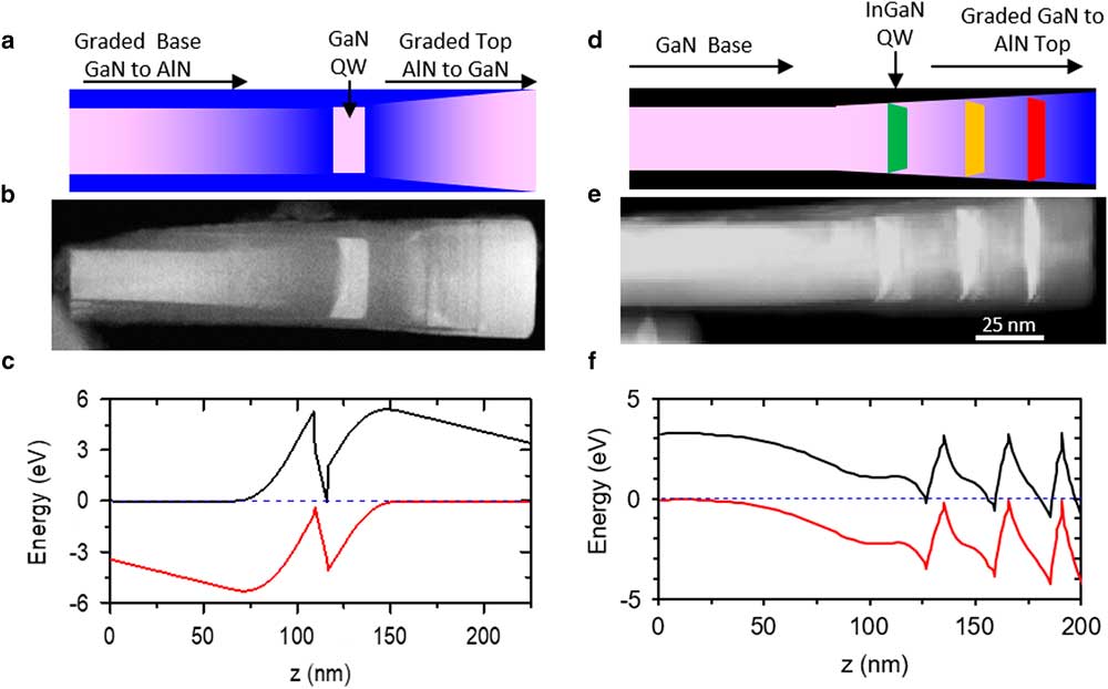
The two nanowire heterostructures, schematics for which are provided in Figure 1, were grown using self-assembled, catalyst-free nanowires by plasma-enhanced MBE (Veeco GEN930, Plainview, NY, USA). Details of the nanowire growth can be found elsewhere (Carnevale et al., Reference Carnevale, Kent, Phillips, Sarwar, Selcu, Klie and Myers2013; Sarwar et al., Reference Sarwar, Carnevale, Yang, Kent, Jamison, McComb and Myers2015). Both epitaxial structures were grown on (111)-oriented Si wafers. Initial pure GaN nanowire nucleation was performed at 720°C for 5 min. For the simple single GaN QDisk sample (hereafter “1×GaN”), following initial nucleation the nanowire growth proceeded via a 100-nm thick linear compositional grade from GaN to AlN, followed by the deposition of 10 nm GaN, and reverse 100-nm thick AlN-to-GaN compositional grading, all at 790°C. The epitaxial structure of the 1×GaN nanowires, a representative high-angle annular dark-field (HAADF) STEM image, and calculated energy band diagram (via BandEng, 2007) are presented in Figures 1a to 1c, respectively. For the triple InGaN QDisk sample (hereafter “3×InGaN”), 150 nm of pure GaN nanowire growth at 790°C proceeded the nucleation step, followed by 120-nm thick GaN-to-AlN compositional grading. Within the 120 nm graded region, three equally spaced (nominally 20 nm) InGaN QDisks were inserted with a cap layer of AlN on the nanowire as a whole. To produce different InGaN compositions (and thus band gaps) for each QDisk, the InGaN growths were performed at three different substrate temperatures: 650°C, 600°C, and 550°C, from bottom to top, respectively. The epitaxial structure of the 3×InGaN nanowires, a representative STEM-HAADF image, and calculated energy band diagram are presented in Figures 1d to 1f, respectively. Due to the N-face polarity of both nanowire structures, GaN-to-AlN grading induces an effective n-type conductivity, whereas AlN-to-GaN yields p-type behavior; in the case of the 1×GaN structure, a p-n junction results, with the QDisk at the junction, yielding a so-called polarization-doped LED. More details of the nanowire growth method can be found Carnevale et al. (Reference Carnevale, Kent, Phillips, Sarwar, Selcu, Klie and Myers2013) and Sarwar et al. (Reference Sarwar, Carnevale, Yang, Kent, Jamison, McComb and Myers2015).

Figure 1 a: Schematic representation of polarization-induced nanowire light-emitting diode (PINLED) heterostructure (GaN×1). b: High-angle annular dark-field (HAADF)-scanning transmission electron microscope (STEM) image of a single PINLED with Z contrast revealing Ga-rich (lighter) and Al-rich (darker) AlGaN regions. c: Calculated energy band diagram along the length of the nanowire. d: Schematic representation InGaN quantum well (QW) heterostructure (InGaN×3). e: HAADF-STEM image InGaN QDisk structure with Z contrast revealing brighter regions (In). f: Calculated energy band diagram along the length of the nanowire.
Results
Figure 2 presents HAADF-STEM and CL data taken from single nanowires representative of each structure type. It is important to note that most of the nanowires did not emit, or had emission processes below the detection limit of the CL detector. For the sufficiently bright nanowires shown in Figure 2, CL spectra were acquired at multiple points along the wire lengths as indicated by the red lines in the HAADF images (Figs. 2a, 2e). The CL spectra obtained were fitted with Gaussian functions to enable extraction of characteristic metrics, including peak intensity and peak center energy (Fig. 2). For the 1×GaN sample, it should be noted that the as-collected HAADF and CL data were found to be slightly misaligned due to specimen drift resulting from the cryogenic sample temperature (from vibrations caused by the liquid nitrogen boiling) and fast acquisition times. Based upon device modeling, the region within the structure with the largest probability of electron-hole recombination, and thus light emission, is at the right-hand edge (in Fig. 2a) of the QDisk. Therefore, this was used as the point of alignment.
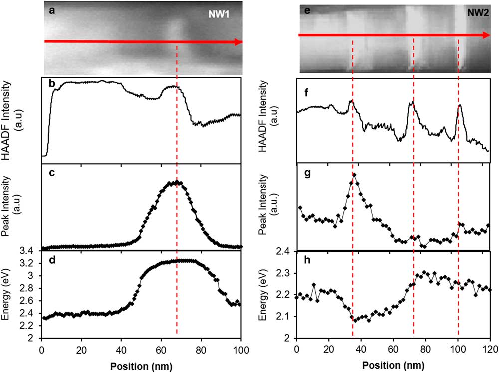
Figure 2 a: High-angle annular dark-field (HAADF)-scanning transmission electron microscope (STEM) image of nanowire 1 with arrow marking region of CL scan. b: HAADF intensity, (c) peak intensity, (d) center emission energy, and (e) HAADF-STEM image of nanowire 2 with arrow marking region of cathodoluminescence scan. f: HAADF intensity, (g) peak intensity, and (i) center wavelength.
Discussion
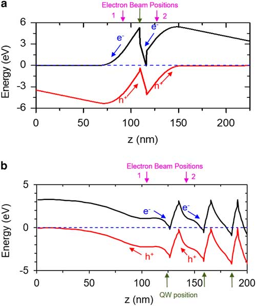
For the 1×GaN structure, the change in peak intensity emission across the QDisk/nanowire interface is more rapid on the right side than the left, as shown in Figure 2c. Linear fits on either side of the QDisk confirm this, as shown in Supplementary Appendix 3. We believe that the asymmetry can be explained by the large electric fields near the QD active regions due to polarization charge, Figure 3a. When the e-beam is incident at location 1 (n-type region), excited holes will drift under influence of the polarization-induced band bending and decay into the QDisk, while the associated beam-generated electrons will drift away from the QDisk. In the case of position 2 (Fig. 3), the opposite behavior is expected, with electrons drifting into the QDisk and holes drifting away. Therefore, when the e-beam is providing carrier generation outside the QDisk itself, CL emission from the QDisk will be limited by the probability of the majority carriers to overcome the sizable (~2 eV) energy barriers at the QDisk/nanowire interfaces. That diffusion probability is limited by the minority electron diffusivity, which is determined by the minority carrier lifetime and mobility. As the diffusivity and mobility of electrons are two to three times larger than that of holes, higher injection efficiency, increased overall radiative efficiency, and therefore brighter CL is expected at position 1 compared with position 2. This diffusive asymmetry of the majority carriers explains why CL intensity decreases at a faster rate on the right side of the quantum well than it increased on the left. The asymmetry seen in peak intensity for this AlN/GaN heterostructures is consistent with a previous report of intensity across a well (Tizei et al., Reference Tizei, Meuret, March, Hestroffer, Auzelle, Daudin and Kociak2014) and a scanning electron microscope-based CL experiment with an InGaN well in a GaN nanorad (Zhuang et al., Reference Zhuang, Bruckbauer, Shields, Edwards, Martin and Allsopp2014). This has also been observed in InGaN quantum dots within GaN using a STEM-CL setup, although without a clear physical explanation of the observed asymmetry (Tourbot et al., Reference Tourbot, Bougerol, Glas, Zagonel, Mahfoud, Meuret, Gilet, Kociak, Gayral and Daudin2012).

Figure 3 a: Energy band diagram along the length of the GaN×1 nanowire and (b) InGaN×3 nanowire.
The trend in emission energy for the 1×GaN sample is consistent with the trend seen with CL intensity (Fig. 2d). This is consistent with an asymmetry in the carrier injection efficiency of the nanowire LED heterostructures. At injection position 1, shown in Figure 3a, the e-beam excitation leads to a larger nonequilibrium carrier density within the QDisks than at position 2 (i.e., larger parasitic recombination at position 2). Therefore, at position 1, there is an increased screening of the polarization field within the QDisk, and a corresponding increase in emission energy, the same effect [elimination of the quantum-confined Stark effect (QCSE)] which is observed under current injection in almost all polar III nitride LEDs. As indicated, the CL intensity decreases with a decrease in emission energy. The emission energy shift is nonlinear with intensity. The emission energy shift with intensity, shown in Figure 4a, is in good agreement with previous work which also indicated about a 1 eV shift with current (Carnevale et al., Reference Carnevale, Kent, Phillips, Sarwar, Selcu, Klie and Myers2013). In other work, it has been shown that blue shifts are also observed for thicker GaN/AlN Qdisks (>4 nm), consistent with what is shown here, and that for thinner Qdisks (<3 nm), the blue shift is near absent, interpreted as being due to negligible QCSE at such length scales (Zagonel et al., Reference Zagonel, Tizei, Vitiello, Jacopin, Rigutti, Tchernycheva, Julien, Songmuang, Ostasevicius, de la Peña, Ducati, Midgley and Kociak2016).
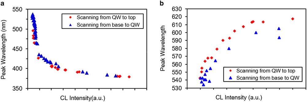
Figure 4 a: Comparing peak wavelength of cathodoluminescence (CL) emission as a function of CL intensity when scanning regions of the nanowire above and below the GaN quantum well (QW) for GaN×1. b: Comparing peak wavelength of CL emission as a function of CL intensity when scanning regions of the nanowire above and below the “green” InGaN QW for InGaN×3.
Given the epitaxial structure and associated band structure of the 3×InGaN sample, the CL emission behavior around the QDisks was expected to be asymmetric. As shown in Figure 2g, this was found to be the case (see Supplementary Appendix 3 for analysis). However, it was also discovered that CL emission originated from only one of the three InGaN QDisks. This corresponded to the QDisk with the lowest In content (i.e., highest growth temperature) and thus the widest band gap; this QDisk also happened to be the deepest within the nanowire. This was true for all nanowires examined that provided sufficiently strong emission—in this case, six other nanowires. One possible explanation for the lack of emission in the other two QDisks is their relative proximity to the nanowire surface, resulting in very efficient surface recombination even when directly exciting within the QDisks. However, this explanation is unlikely, as the emission observed is based on transmission through the sample, so surface recombination factors should play a smaller role.
For the QDisk that did emit, there is also an observed asymmetry in peak intensity, as indicated in Figure 2g. For this structure, the peak intensity increases rapidly from the bottom of the QDisk toward its center, while it declines more slowly toward the nanowire top, the opposite to the asymmetry seen in the 1×GaN nanowire sample. This reversal is fully consistent with the expected band diagram as the polarization field within InGaN/(Al)GaN QDisks is opposite that of the AlN/GaN QDisks. For nanowire ensemble sample 2, as shown in Figure 3b, if the electron beam is below the QDisk, the holes must diffuse uphill to be injected into the QDisk. If the electron beam is placed above the QDisk, the generated holes drift into the QDisk. Thus, at a given distance from the QDisk, brighter CL occurs when the e-beam is above rather than below the QDisk.
The opposite CL energy-intensity relationship is observed for the 3×InGaN nanowire sample compared with that of 1×GaN sample. Although we expect a blue shift trend for this QDisk with increasing carrier density, which is demonstrated here by CL intensity, instead a red shift is observed, as shown in Figures 2h 4b. Taken at face value, this observation implies that although there are more carriers present for screening, the polarization distortion increases with increased carrier injection, which cannot be explained by the simple one-dimensional (1D) band edge diagram. It is also worth noting that red shifting was not observed in the work by Zagonel et al., regardless of size of the Qdisk (Zagonel et al., Reference Zagonel, Tizei, Vitiello, Jacopin, Rigutti, Tchernycheva, Julien, Songmuang, Ostasevicius, de la Peña, Ducati, Midgley and Kociak2016). Although polarization effects are only expected along the z-direction (c-axis), the three-dimensional (3D) nature of the heterostructures can also generate radial polarization effects, even along intrinsically nonpolar directions within the basal plane of wurtzite. A full 3D band structure must be considered, where the radial strain profile is known to generate additional piezoelectric polarization dipoles that lead to radial electric fields that separate injected electrons and holes within the QDisks (Sarwar et al., Reference Sarwar, May, Chisholm, Duscher and Myers2016). In those studies, the gradual nanowire taper results in a strain distribution that varies along the nanowire axis, which leads to a variation in the radial piezoelectric polarization between QDisks inserted at different positions along the nanowire. In that case, each QDisk exhibits different QCSE. This variation might explain the lack of emission from the other two QDisks. Also, the fact that injected carriers are separated in both axial and radial directions implies that the screening effect expected in 1D may not hold in the 3D case. Additional nano-CL mapping along the radial direction within the QDisks might be used to explore such effects.
It is important to consider the limitations of STEM-CL for anomalous results like these. The work by Zagonel et al. to explore carrier recombination within individual GaN/AlN QDisk superlattices demonstrated that STEM-CL can be used in part to understand the emission spectra from ensembles of QDisks (Zagonel et al., Reference Zagonel, Mazzucco, Tencé, March, Bernard, Laslier, Jacopin, Tchernycheva, Rigutti, Julien, Songmuang and Kociak2011). Still, the observed superlattice inhomogeneity, which is consistent with other reports, demonstrates the limitations of STEM-CL studies, while partially explaining the low efficiency of III-N nanowire LEDs. Some QDisks emit individually, while others emit collectively, and some nanowires do not emit at all. There is no current explanation for this outside of potential compositional nonuniformities as explained by EL studies showing not all wires emitting (Kaganer et al., Reference Kaganer, Jenichen, Brandt, Fernández-Garrido, Dogan, Geelhaar and Riechert2012; Zettler et al., Reference Zettler, Corfdir, Geelhaar, Riechert, Brandt and Fernández-Garrido2015). It is possible the electron beam damage causes some nanowires to not emit, but because nanowires in this experiment were all exposed to the same minimal beam exposure before data collection, it seems unlikely that electron beam damage causes this entire discrepancy. A correlation between emission and compositional/structural features has not been made, and this information will be vitally important towards the advancement of nanowire-based applications.
Summary
In conclusion, STEM-CL spectra from electron and hole recombination within individual QDisk active regions of nanowire LED heterostructures were studied. Most of the nanowires in this study did not emit above the detection limit of the CL detector, which indicates that the detection limit on the CL detector is not high enough for these nanowires or that compositional nonuniformities, such as defects or interfaces, in these nanowires lead to inconsistent emission results, as previously found with EL studies. If the latter is true, this also further explains, in part, the low efficiency of such nanowire-based devices. For the nanowires that did emit, we observe a spatial asymmetry in the carrier trapping process, as indicated by the asymmetric intensity changes and spectral shifting for carriers injected at the same distance from the QDisk active region. The results are consistent with the polarization-induced electric fields in the barrier regions of the nano-LEDs, and reflects the imbalance in hole versus electron diffusivity in AlGaN. Furthermore, in AlN/GaN QDisk active regions, the spectral shifting is identical to what is observed in the EL of such active regions, demonstrating that the nano-CL can also be used to probe carrier injection induced screening and other nonlinear phenomena within QDisk active regions. In InGaN/AlGaN QDisks, the same carrier trapping asymmetry is observed as indicated by the variation in CL intensity, however the spectral shifting in these active regions cannot be explained by a simple 1D picture. In addition, the fact that two QDisks did not emit in the 3×InGaN sample is not currently explainable by the current understanding of nanowire device physics. In addition, studies in the past have found similar results with either combined emission from multiple wells, or some well inexplicably having nonemission in a nanowire that otherwise emits. We suspect that further nano-CL studies on such active regions might be able to map out the radial variations within the nanowire LED active regions to help identify the 3D details of the band diagram. Such details are essential in identifying parasitic nonradiative recombination pathways and developing optimal nanowire photonic devices, but improvements in CL detection in the STEM will go a long way in understanding these roles. This is especially important in the nascent field of nanoplasmonics coupled to semiconductor optoelectronics, where nm-scale carrier trapping and recombination must be precisely engineered to achieve coupling to the plasmonic modes within metal coatings or particles.
Supplementary Material
To view supplementary material for this article, please visit https://doi.org/10.1017/S143192761800017X
Acknowledgments
D.W.M. acknowledges support from the Ohio Third Frontier and The Ohio State University, as well as a Facilities Grant from the Institute for Materials Research (IMR) at The Ohio State University. The authors would first like to acknowledge Dr. David Stowe and Gatan UK for the provision of the Vulcan system to CEMAS under an evaluation agreement to make these measurements possible. This work was partially supported by the Army Research Office (W911NF-13-1-0329) and by the National Science Foundation CAREER Award no. DMR-1055164. S.D.C. acknowledges support from the National Science Foundation Graduate Research Fellowship Program (2011101708).