Hostname: page-component-76fb5796d-22dnz Total loading time: 0 Render date: 2024-04-25T07:37:37.112Z Has data issue: false hasContentIssue false

Need for Large-Area EDS Detectors for Imaging Nanoparticles in a SEM Operating in Transmission Mode

Published online by Cambridge University Press:  27 August 2014

Steffi Rades
Affiliation:
BAM Federal Institute for Materials Research and Testing, Division 6.8 Surface Analysis and Interfacial Chemistry, Berlin, Germany.
Tobias Salge
Affiliation:
Bruker Nano GmbH, Berlin, Germany.
Roland Schmidt
Affiliation:
Hitachi High-Technologies Europe GmbH, Krefeld, Germany.
Vasile-Dan Hodoroaba
Affiliation:
BAM Federal Institute for Materials Research and Testing, Division 6.8 Surface Analysis and Interfacial Chemistry, Berlin, Germany.

Abstract

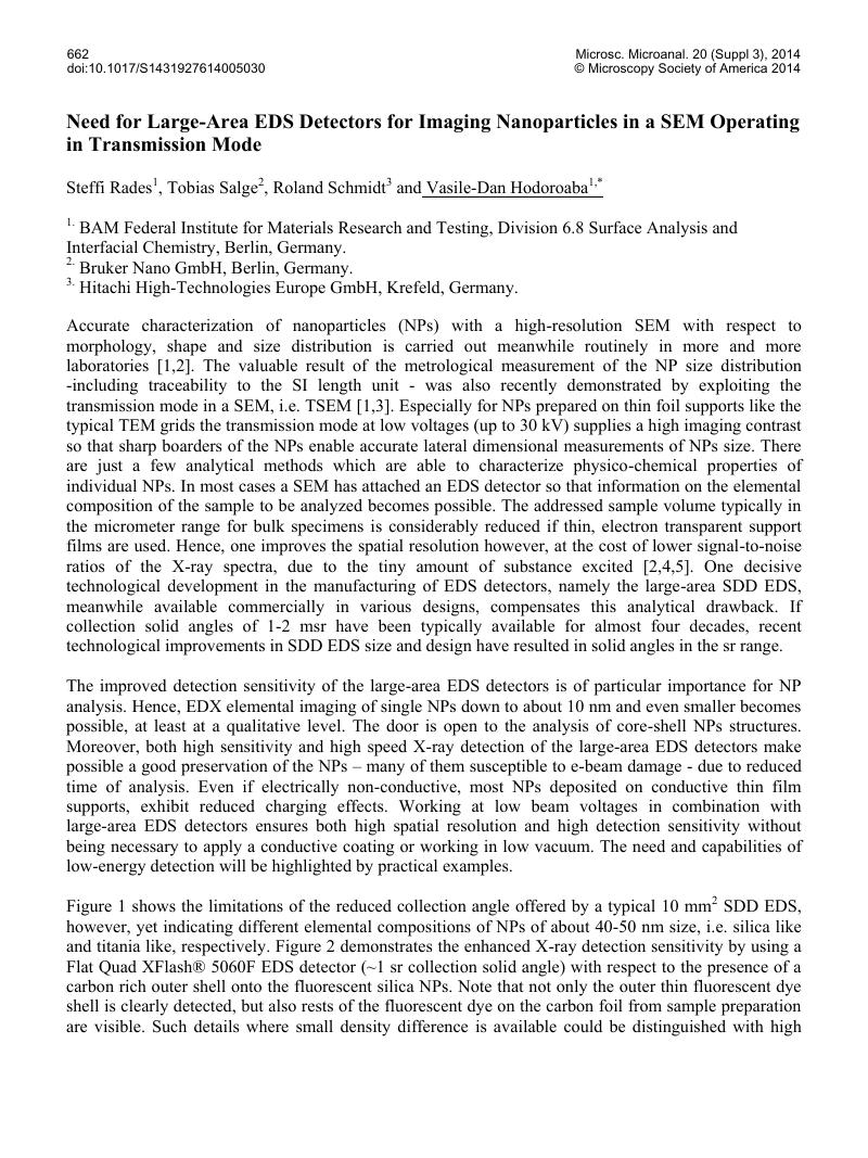
Image of the first page of this content. For PDF version, please use the ‘Save PDF’ preceeding this image.'
Type
Abstract
Copyright
Copyright © Microscopy Society of America 2014 

References

[1] Buhr, E, Senftleben, N, et al., Meas. Sci. Technol. 20 (2009), p. 413.Google Scholar
[2] Hodoroaba, V-D, Benemann, S, et al., Microsc. Microanal. 18 (Suppl 2) (2012), p. 1750.Google Scholar
[3] Motzkus, C, Macé, T, et al., J. Nanopart. Res. 152013), p. 1919.Google Scholar
[4] Hodoroaba, V-D, Akcakayiran, D, et al., Analyst (2014), in press.Google Scholar
[5] Hodoroaba, V-D, Rades, S, et al., Surf. Interf. Anal (2014), in press.Google Scholar
[6] The research leading to these results has received funding from the European Union’s Seventh Framework Programme (FP7/2007-2013) under grant agreement n° 263147 (NanoValid - Development of reference methods for hazard identification, risk assessment and LCA of engineered nanomaterials).Google Scholar