


Introduction
Due to their unique optical and electrical properties, 2D materials recently gained increasing attention. Many of these properties can be linked to the topography and local strain of mono- and few-layer crystals. Tuning the band gap of semiconducting 2D materials can be achieved by tension and compression (Manzeli et al., Reference Manzeli, Allain, Ghadimi and Kis2015; Island et al., Reference Island, Kuc, Diependaal, Bratschitsch, van der Zant, Heine and Castellanos-Gomez2016; Gant et al., Reference Gant, Huang, de Lara, Guo, Frisenda and Castellanos-Gomez2019). Light absorption properties are influenced by ripple formation (Miró et al., Reference Miró, Ghorbani-Asl and Heine2013; Zhu & Johnson, Reference Zhu and Johnson2018). Single-photon emitters in some transition metal dichalcogenides (TMDC) are likely to be related to local strain (Tonndorf et al., Reference Tonndorf, Schmidt, Schneider, Kern, Buscema, Steele, Castellanos-Gomez, van der Zant, de Vasconcellos and Bratschitsch2015; Kern et al., Reference Kern, Niehues, Tonndorf, Schmidt, Wigger, Schneider, Stiehm, Michaelis de Vasconcellos, Reiter, Kuhn and Bratschitsch2016; Zheng et al., Reference Zheng, Chen, Huang, Gogoi, Li, Li, Trevisanutto, Wang, Pennycook, Wee and Quek2019). Even electric conductance (Miró et al., Reference Miró, Ghorbani-Asl and Heine2013) and band-piezoelectric effects (Dai et al., Reference Dai, Zheng, Zhang, Wang, Lin, Li, Hu, Sun, Zhang, Qiu, Fu, Cao and Hu2019) can be tailored by applying strain.
Transmission electron microscopy (TEM) allows to measure strain on various scales and with different accuracies (Cooper et al., Reference Cooper, Denneulin, Bernier, Béché and Rouvière2016). In particular, diffraction-based methods are known for their high precision, since they are not limited by spherical and chromatic aberrations. All these methods, with the exception of precession electron diffraction, have one thing in common: The interpretation of strain is based on a single projection of the structure along the direction of the incident beam. Few or monolayers, on the other hand, have no periodicity in the third dimension. In the case of graphene or monolayer boron nitride, the thickness reduces to the size of a single atom. Additionally, these 2D materials exhibit a wavy topography when prepared on top of a substrate (Deng & Berry, Reference Deng and Berry2016; Han et al., Reference Han, Nguyen, Cao, Cueva, Xie, Tate, Purohit, Gruner, Park and Muller2018) or freely suspended (Meyer et al., Reference Meyer, Geim, Katsnelson, Novoselov, Booth and Roth2007). This can falsify the strain measurement, when using for instance nano beam electron diffraction (NBED)-mapping or geometric phase analysis of high-resolution TEM images. If the sample is tilted in one direction with respect to the incident electron beam, the projected lattice will appear compressed in the direction perpendicular to the tilting axis.
A statistical approach can be used to evaluate tilted electron beam diffraction patterns of larger regions. Due to the many different surface orientations, the reciprocal lattice will resemble a cone-shaped structure (Meyer et al., Reference Meyer, Geim, Katsnelson, Novoselov, Booth and Roth2007). Measuring the positions, intensity distribution, and ellipticity of the resulting tilted diffraction pattern spots, the mean strain and the mean topographical appearance of the sample can be described (Ludacka et al., Reference Ludacka, Monazam, Rentenberger, Friedrich, Stefanelli, Meyer and Kotakoski2018). Scanning approaches to this method have also been used (Uesugi, Reference Uesugi2013; Sickel et al., Reference Sickel, Asbach, Schneider, Bratschitsch and Kohl2019).
Another method to measure local strain in monolayers is convergent beam electron holography (Latychevskaia et al., Reference Latychevskaia, Hsu, Chang, Lin and Hwang2017, Reference Latychevskaia, Woods, Wang, Holwill, Prestat, Haigh and Novoselov2019). Local variations of the atomic positions lead to intensity variations inside the diffraction discs of the defocused convergent beam electron diffraction (CBED) pattern. In general, a reconstruction of the atomic positions of monolayers using CBED is not possible due to the lack of quantitative phase informations. Furthermore, the distinction of in- and out-of-plane variations can sometimes be challenging (Latychevskaia et al., Reference Latychevskaia, Woods, Wang, Holwill, Prestat, Haigh and Novoselov2018).
Han et al. (Reference Han, Nguyen, Cao, Cueva, Xie, Tate, Purohit, Gruner, Park and Muller2018) used NBED-mapping to measure strain and topography in a 2D material. They took only one NBED-map and calculated the strain from the spot positions without taking the influence of the topography into account. The shapes of the diffraction spots were used to gather relative information about the local topography which afterwards were calibrated by an atomic force microscopy measurement, which determined the maximum slope of the sample. This method required a combination of different techniques to be quantitative and the probe size needed to be large enough to detect topographical changes within the diffraction spots.
We present an electron diffraction technique, which is capable of disentangling local strain and topography in 2D materials quantitatively. After introducing the theoretical concept, simulations of a MoS2 monolayer demonstrate the capabilities of the method. For the chosen simulation parameters, the entire information about the lattice strain and topography is recovered. Furthermore, we provide an experimental proof of concept at a fold of a freely suspended WSe2 monolayer together with a discussion of the accuracy of the method.
Method and Simulations
Theoretical Concept
The absence of a periodic continuation in the third dimension of an atomically thin (2D) material results in a large extension of the structure factor in that direction, so that the shape of the reciprocal lattice spots becomes rod-like (Reimer, Reference Reimer1984; Meyer et al., Reference Meyer, Geim, Katsnelson, Novoselov, Booth and Roth2007). In contrast to bulk (3D) samples, where the Ewald sphere only intersects a few reciprocal lattice spots in the plane perpendicular to the direction of the incident beam, the Ewald sphere of a 2D sample always intersects all rods inside the sphere within a large tilting range. In real space, this implies a projection. Thus, lattice directions in the plane are visible, even if they are not perpendicular to the direction of the incident beam. If the sample is tilted by an angle β, the projection of a lattice period a is given by a · cos β. Thus, the lattice appears to be compressed (see Fig. 1a). The diffraction spots of the corresponding measurement are farther apart, because the lattice rods are no longer perpendicular to the Ewald sphere (see Fig. 1b). Hence, for a correct strain measurement, it is necessary to know the local slope of the 2D sample with respect to the incident beam direction.
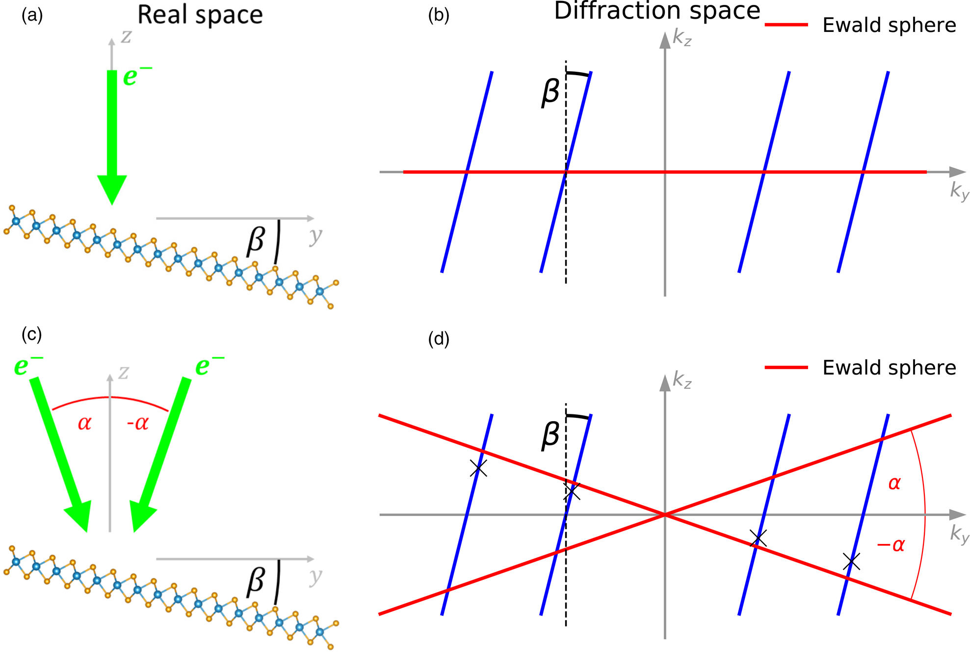
Fig. 1. (a) Electron beam and tilted sample in real space and (b) Ewald construction of the 2D crystal in diffraction space. The local orientation differs from the mean lattice by the angle β. (c,d) The same sample with an incident electron beam tilted by angle the ± α. The ×-marked positions on the rods indicate the shortest distances to the coordinate origin and thus the positions for the strain determination. Since the wavelength of an electron beam in a TEM is typically more than one order of magnitude smaller than the lattice constant, the Ewald sphere can be approximated locally by a plane.
The method introduced here solves this problem by performing two diffraction measurements with different specimen tilts (+α and −α in Figs. 1c and 1d), to obtain full information about the locations of the diffraction rods. Calculating the rod positions provides the strain and calculating the orientation of the rods the local slope of the sample. Figures 1c and 1d show the measuring concept in real and diffraction space. For the sake of clarity, the incident beam in Figure 1 was tilted with respect to the sample.
The topography and strain calculations are demonstrated by two NBED-maps tilted around the x-axis at angles α = α p and −α = α m. The p and m stand for plus and minus in this example. In principle, one is not bound to certain tilting directions or angles.
First, the positions P′ = (p x′, p y′) and M′ = (m x′, m y′) of the spots on the diffraction pattern are determined. The position of the intersection between the Ewald sphere and the diffraction rods in reciprocal space can then be calculated as shown in Figure 1d.
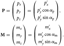 $$\eqalign{{\bf P} & = \left(\matrix{\,p_x \cr p_y \cr p_z }\right) = \left(\matrix{\,p_x' \cr p_y' \cos \alpha_{\rm p} \cr p_y' \sin \alpha_{\rm p} }\right),\cr {\bf M} & = \left(\matrix{m_x \cr m_y \cr m_z }\right) = \left(\matrix{m_x' \cr m_y' \cos \alpha_{\rm m} \cr m_y' \sin \alpha_{\rm m} }\right).}$$
The slope of the rod is now given by R = P − M. With that the tilt of the rod with respect to the unity vector N in k x and k y direction can be calculated
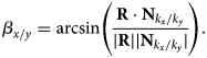 $$\beta_{x/y} = \arcsin \left({ {\bf R} \cdot {\bf N}_{k_x/k_y}\over \vert {\bf R} \vert \vert {\bf N}_{k_x/k_y} \vert} \right).$$
The height information is reconstructed from the slopes by an algorithm from Frankot and Chellappa (Frankot & Chellappa, Reference Frankot and Chellappa1988; Quéau et al., Reference Quéau, Durou and Aujol2018).
The base points of the rods with the coordinate origin, which are indicated by ×-marks in Figure 1d, is given by
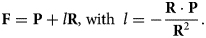 $${\bf F} = {\bf P} + l{\bf R},\; \hbox{with}\ \, l = -{{\bf R}\cdot {\bf P}\over {\bf R}^{2}}.$$
Using F, the strain can be calculated without the influence of the topography. The lattice strain between two opposite diffraction rods is given by
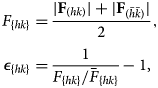 $$\eqalign{F_{\{ hk\} }& = {\vert {\bf F}_{( hk) } \vert + \vert {\bf F}_{( \bar{h}\bar{k}) } \vert\over 2},\cr \epsilon_{\{ hk\} }& = {1\over F_{\{ hk\} }/ \bar{F}_{\{ hk\} } } -1, }$$
where  $\bar {F}_{{ hk} }$ is the mean value of a reference area. The projected angle between two lattice directions ${\it F}_{\angle ( { h_1k_1} , { h_2k_2} ) }$ is given by the angle between two base point pairs
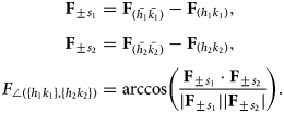 $$\eqalign{{\bf F}_{\pm s_1} & = {\bf F}_{( \bar{h_1}\bar{k_1}) }-{\bf F}_{( h_1 k_1) }, \cr {\bf F}_{\pm s_2} & = {\bf F}_{( \bar{h_2}\bar{k_2}) }-{\bf F}_{( h_2 k_2) },\cr F_{\angle( \{ h_1k_1\} , \{ h_2k_2\} ) }& = \arccos \left({{\bf F}_{\pm s_1}\cdot {\bf F}_{\pm s_2}\over \vert {\bf F}_{\pm s_1} \vert \vert {\bf F}_{\pm s_2}\vert } \right).}$$
The relative angular changes, with respect to the mean value of a reference region  $\bar {F}_{\angle ( { h_1k_1} , { h_2k_2} ) }$, are given by
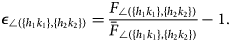 $$\epsilon_{\angle( { h_1k_1} , { h_2k_2} ) } = {F_{\angle( { h_1k_1} , { h_2k_2} ) }\over \bar{F}_{\angle( { h_1k_1} , { h_2k_2} ) }} -1.$$
The strain can then be transformed into a Cartesian coordinate system with tensile strain in the x- and y-direction εxx, εxy, shear strain εxy and lattice rotation Θ (Zuo & Spence, Reference Zuo and Spence2017).
 $$\mathfrak{T} = \left(\matrix{1 + \epsilon_{xx} & {1\over 2}( \epsilon_{xy}-\Theta) \cr {1\over 2}( \epsilon_{yx} + \Theta) & 1 + \epsilon_{yy} \cr }\right)$$
In the following simulations and measurements, the sample is tilted. This yields equivalent results, since only the angle of the incident electron beam relative to the surface normal of the sample is relevant.
Extracting Topography and Strain Information from Simulated 2D Samples
We first demonstrate the concept for simulated TMDC monolayers. As an example, we choose 1H-MoS2, since suitable force field data are available to simulate freely suspended MoS2 monolayers (Ostadhossein et al., Reference Ostadhossein, Rahnamoun, Wang, Zhao, Zhang, Crespi and Van Duin2017). The different test structures are created in two steps. Starting with a flat monolayer, the z-coordinates of the atom positions are modulated by the values of the desired topography. In a second step, the atoms are shifted in the x-, y-, and z-directions to minimize the total potential energy. For this purpose, we use the molecular dynamics (MD) simulation program LAMMPS (Plimpton, Reference Plimpton1993) with the reactive force field specially designed for MoS2 monolayers (Ostadhossein et al., Reference Ostadhossein, Rahnamoun, Wang, Zhao, Zhang, Crespi and Van Duin2017). To prevent the relaxation into a nonwavy configuration, the size of the simulation box is chosen slightly smaller than the corresponding flat structure.
The NBED patterns are simulated using a multi-slice code from Kirkland (Reference Kirkland1998). The simulations are carried out in three steps. First, a probe wave function is simulated, then the propagation of the wave through the test structures and finally the resulting image is calculated. The size of the diffraction patterns is set to 2,048 × 2,048 pix, the acceleration voltage to 60 kV, C30 to 1.2 mm, C50 to 0 mm, and the 2-fold astigmatism to 0 Å. The defocus, the objective aperture semiangle, and the C23 values are set according to the different simulation parts. The slice thickness is set to 1 Å and thermal vibrations are included with 300 K and an average over 10 runs. Note that the test structures are not tilted with the crystal tilt option within the Kirkland code. The input file contains the already tilted atom positions. The position of the diffraction spots is determined by cross-correlation with a template (Ozdol et al., Reference Ozdol, Gammer, Jin, Ercius, Ophus, Ciston and Minor2015).
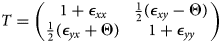
As a first step, two test structures consisting of a MoS2 monolayer with a Gaussian-shaped wrinkle of different dimensions are created, as sketched in Figure 2a. Wrinkle 1 has an amplitude of A = 1 nm and a width of σ = 6 nm, which results in a maximum slope of approx. 6°. Wrinkle 2 has an amplitude of A = 1.5 nm and a width of σ = 2 nm, which results in a maximum slope of approx. 20°. In order to evaluate the influence of the electron probe size (see Fig. 11e for details), the slopes of the two wrinkles are calculated by two simulated NBED line scans at tilts of α = ±10° for different objective aperture sizes, as shown in Figures 2b and 2c. Figure 2d shows the mean absolute error to the slope obtained by the Mo atom positions (black line in Figs. 2b and 2c). For the flatter Gaussian wrinkle 1, the influence of the probe size is negligible for aperture sizes larger than 3 mrad. For the steeper Gaussian wrinkle 2, the deviation is larger than 1.2° for all probe sizes and the highest values are at the smallest and largest probe sizes. At larger probe sizes, the irradiated area includes a larger range of different slopes. For a probe diameter of 1 nm, the slope range within the two test structures can amount up to 1.5° for the flatter Gaussian wrinkle and over 10° for the steeper Gaussian wrinkle. Hence, the resulting diffraction spots are blurred according to the surface normal variations of the local structure, as will be discussed in detail in the section “Influence of the beam limiting aperture and aberrations”. For large objective apertures, the convergence angle becomes larger than the Bragg angle. Here, objective apertures larger than 8 mrad at 60 kV lead to an overlap of the diffraction discs. At larger tilts of the surface normal with respect to the incident beam, this can already happen at slightly smaller apertures, which can significantly hamper the spot position detection.
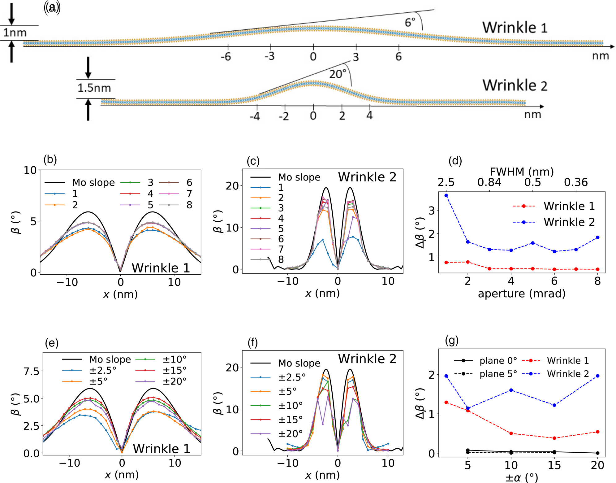
Fig. 2. (a) Simulated MoS2 monolayers with a Gaussian-shaped wrinkle in the zigzag direction. Wrinkle 1 has an amplitude of A = 1 nm and a width of σ = 6 nm and wrinkle 2 has an amplitude of A = 1.5 nm and a width of σ = 2 nm. Slope of wrinkle 1 and wrinkle 2, calculated by the Mo atom positions (black line) and from NBED-maps with objective apertures from 1 to 8 mrad, for a sample tilt of α = ±10° (b,c) and with sample tilts from ± 2.5° to ± 20°, for an objective aperture of 5 mrad (e,f). Mean absolute error between the slopes calculated from the known Mo positions and the simulated NBED maps for different objective apertures with α = ±10° are shown in (d) and for different tilting angles with an objective aperture of 5 mrad are shown in (g). The probe diameters resulting from the different convergence angles are displayed on the second scale on top of (d). As a reference in (g), a flat monolayer with an angle of β = 0° and β = 5° is simulated as well (black lines).
In Figures 2e–2g, the tilt angles used to calculate the slopes of the diffraction rods are compared at a fixed objective aperture size of 5 mrad. As a reference, two flat test structures (without a wrinkle) which are inclined by 0° and 5° are analyzed as well. Their maximum mean absolute error value is below 0.1°. The flatter Gaussian wrinkle tends to settle around Δβ = 0.5° for tilting angles above ±10°. The values of the steeper Gaussian wrinkle varies around a value of Δβ = 1.5°. This indicates that the accuracy for high slopes is not primarily limited by the choice of tilting angles.
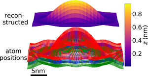
Next, the topography of a Gaussian type test structure will be recovered in both the x- and y-directions. Figure 3a gives an overview of the atom positions of the test structure and the reconstructed height map in comparison. Since the atomic positions of the original 2D Gaussian structure are slightly altered due to the energy minimization within the MD simulation program, small wrinkles near the edges of the structure form, and the threefold symmetry of the lattice causes small deviations from the rotational symmetry. In Figure 3b, the corresponding slope map is shown, which is calculated from two NBED-maps tilted by α p/m = ±10° around the x-axis. Figures 3c–3e provide cross-sections of reconstructions with tilting angles ranging from ±5° to ±20° in comparison to the height values from the Mo atom positions. The shape of the test structure is evident in every simulation, with better agreements at higher tilting angles, as can also be observed by the mean deviation from the slope and height values from the Mo positions, shown in Figures 3f and 3g.
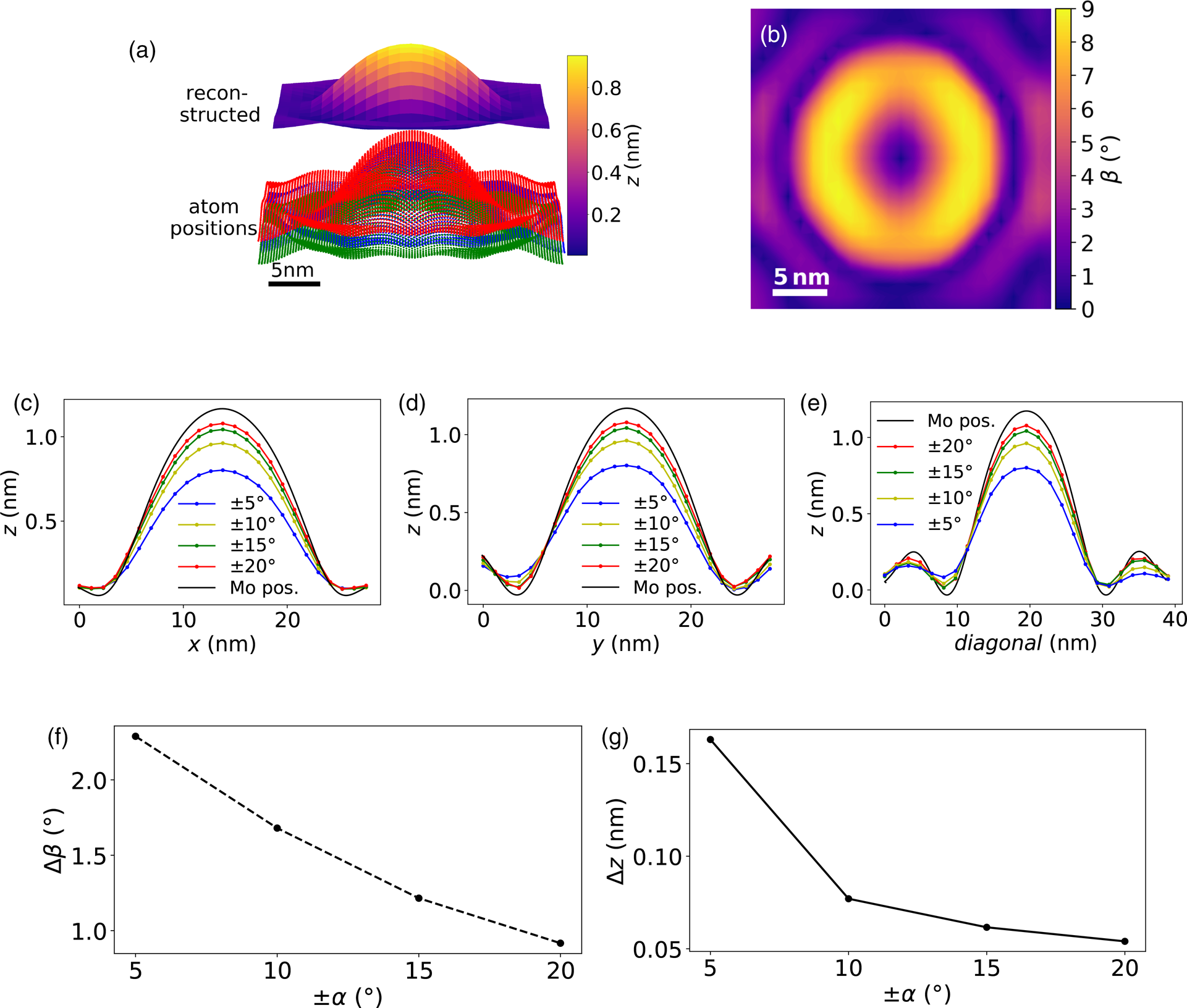
Fig. 3. Reconstructed topography of a Gaussian-shaped MoS2 monolayer. (a) Atomic positions of the Mo atoms (blue) and the upper and lower S atoms (red and green) and above the reconstructed topography. (b) Calculated absolute slope map from two NBED-maps tilted around α p/m = ±10°. (c–e) Cross-sections of the reconstructed height information for α p/m from ± 5° to ± 20° and the z values of the Mo atoms (black lines). Mean absolute errors of the slope Δβ (f) and the height Δz (g) differences between the ones calculated from the Mo positions and the NBED-maps at different tilting angles. The small deviations from the Gaussian shape of the test structure are due to the energy minimization of the MD simulation.
The ground truth strain maps were determined by measuring the unit-cell dimensions centered on the Mo sites. The strain between lattice planes in armchair direction, therefore, corresponds to the distance variations of the adjacent Mo atoms in the perpendicular direction (shown in Fig. 5a). The strain variations between lattice planes in zigzag direction corresponds to distance variations, as sketched in Figure 4a for the {01} direction. The corresponding strain maps are shown in Figures 4c and 5c for the  ${ 2\bar {1}}$ direction. The strain ranges between ${\pm } 0.45\percnt$, which corresponds to lattice spacing variations of ±0.013 Å for a lattice constant of 2.75 Å in zigzag direction and ±0.015 Å for a lattice constant of 3.18 Å in armchair direction. In Figures 4b and 5b, the z-component of the Mo positions were neglected, which is the case for a projection along the z-axis. The range of values is almost twice the size of 4c and 5c, respectively. The largest differences are at the regions with the steepest slopes in strain direction.
Fig. 4. Strain between the lattice planes in the {01} direction. (a) Schematic drawing of the MoS2 lattice (Mo in blue, S in yellow) with the distance between two (10) lattice planes marked in red-black. Strain calculated using only the x- and y-components (b) and using x-, y-, and z-components (c) of the Mo positions. (d) Overview of the diffraction spots with the red-black line marking the distance used for calculating the strain of the NBED-map with α = 0° (e) and the NBED-maps with α p/m = ±10° (f). (g) Diffraction pattern overview with arrows marking the direction of the spot variations used to calculate (h) and (i) from the respective α = 0° and α p/m = ±10° NBED-maps. The tilting axis in (a), (d), and (g) is indicated by a dashed line. The white boxes in (b) and (c) mark the area for the strain reference values of the strain maps, as this area has little strain.
Fig. 5. Strain between the lattice planes in the  ${ 2\bar {1}}$ direction. (a) Schematic overview of the MoS2 lattice (Mo in blue, S in yellow) with the distance between two $( 2\bar {1})$ lattice planes marked in red-black. Strain calculated using only the x- and y-components (b) and using x-, y-, and z-components (c) of the Mo positions. (d) Overview of the diffraction spots with the red-black line marking the distance used for calculating the strain of the NBED-map with α = 0° (e) and the NBED-maps with α = ±10° (f). (g) Diffraction pattern overview with arrows mark the direction of the spot variations used to calculate (h) and (i) from the respective α = 0° and α = ±10° NBED-maps. The tilting axis in (a), (d), and (g) is indicated by a dashed line. The white boxes in (b) and (c) mark the area for the strain reference values of the strain maps, as this area has little strain.
Regarding only the relative distances between two opposite diffraction spots, many similarities can be seen, as shown in Figures 4d–4f for the  $( 01) - ( 0\bar {1})$ distance variations. The strain map obtained from a single NBED map with α = 0° qualitatively matches the appearance of Figure 4b. The strain from the two α p/m = ±10° NBED-maps on the other hand shows smaller values on the upper right and lower left part of the map. The main reason for this is the lattice rotation and shear strain, which are not included when regarding the relative distances of two diffraction spots without taking their azimuthal position variations into account.
A more direct comparison to Figures 4a–4c can be achieved by calculating the tensile strain εxx of the corresponding direction. In contrast to (d–f), εxx is based on the relative position variations of all diffraction spots considered in the selected lattice direction. Here, the strain determined from the α p/m = ±10° NBED-maps resembles the strain in (c) more closely. The maxima of the absolute differences to the real strain values of all three zigzag directions are less then 0.2%. The projected values are two to three times smaller than the strain values from the projected Mo positions in Figure 4b. The reason for this is most likely the finite probe size, which is partly larger than the projected strain variation. This results in an averaging over many diffraction rod positions and orientations (see Section “Accuracy of the technique” for details). In the same way, the angular variations between lattice planes of different directions can be calculated. For example, the angle variations between the {10} and  ${ 1\bar {1}}$ planes in Figures 6a–6c again show the expected angular strain for a projected (b) and for a measurement taking the wrinkled structure into account (c). The angular strain of (c) is within a range of approx. 0.37%, which corresponds to (120.0 ± 0.5)°. In the center of the monolayer, the angular strain is canceled out from every direction. From this position in the direction of the bisector ( ${ 2\bar {1}}$-direction), the angle becomes smaller, which is expected considering the tensile strain in the ${ 2\bar {1}}$-direction is highest in this region, as shown in Figure 5. The projected angles in Figure 6b have mostly opposite strain values compared to (c) in regions where the slope of the simulated sample is steep. If the angle is tilted around the angle bisector (tilt direction is indicated in (a) with i), the projected angle becomes smaller (dark regions in (b) marked with i) and at tilting directions perpendicular to the bisector the projected angle becomes larger (indicated in (a) and (b) with ii).
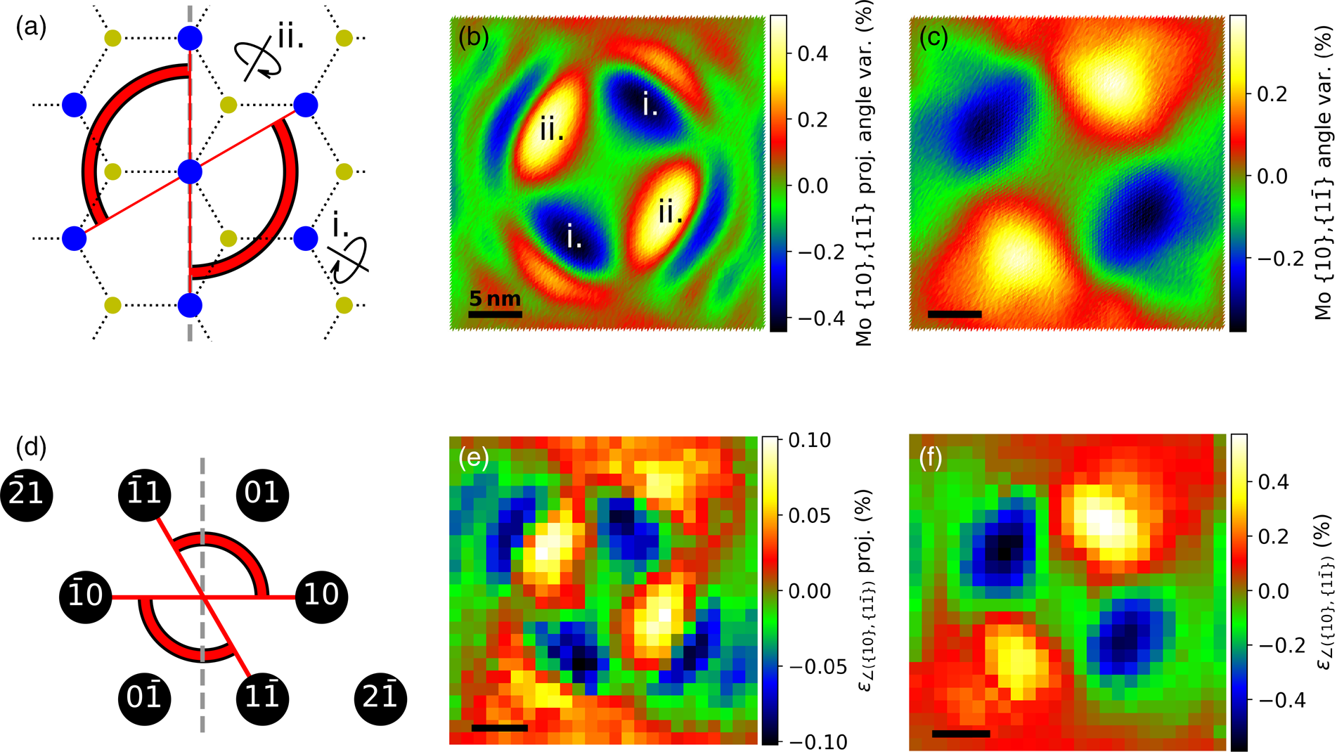
Fig. 6. Bond angle deviation between the {10} and  ${ 1\bar {1}}$ lattice planes. (a) Schematic overview of the MoS2 real space lattice with the position of the measured angle marked red-black. Angular strain calculated using only the x- and y-components (b) and using x-, y-, and z-components (c) of the Mo positions. (d) Overview of the diffraction spots with the red-black lines marking the angles used for calculating the strain of the NBED-map with α = 0° (e) and the NBED-maps with α p/m = ±10° (f). The tilting axis in (a) and (d) is indicated by a dashed line. The indicated lattice rotation directions i and ii in (a) correspond to the dark i and bright ii regions in (b).
The angular variations calculated from the NBED-maps show a similar behavior, as can be seen in Figures 6d–6f. The values of (e) are much smaller than (b). The main reason for this is most likely the same as in the strain value differences of Figures 4b, 4e, and 4h. The values from the α p/m = ±10° maps differ approx. by 0.2°. For this simulation, an angular difference of 0.2° at a first-order diffraction spot corresponds to less than 0.4 pixel. To increase the accuracy, the positions of the diffraction spots of a higher order could be used, at the cost of a lower signal-to-noise ratio.
Sample Preparation and Experimental Setup
A bulk WSe2 crystal (Tonndorf et al., Reference Tonndorf, Schmidt, Böttger, Zhang, Börner, Liebig, Albrecht, Kloc, Gordan, Zahn, De Vasconcellos and Bratschitsch2013) is mechanically exfoliated down to a single layer onto a PDMS gel pack (WF film a Gel-Film© from the company Gel-Pak). The transparent gel pack is mounted on a stamping setup (Castellanos-Gomez et al., Reference Castellanos-Gomez, Buscema, Molenaar, Singh, Janssen, Van Der Zant and Steele2014), which allows for the transfer of a WSe2 monolayer onto a holey silicon nitride grid. To check whether the prepared sample is a monolayer, a photoluminescence (PL) measurement was carried out. Since WSe2 becomes a direct band gap semiconductor during the transition from bi- to monolayer, a strong increase in the PL signal and a spectral shift due to the changed band gap can be measured. Later, the spot intensities of the electron diffraction patterns additionally confirm that it is a monolayer (Wu et al., Reference Wu, Odlyzko and Mkhoyan2014). The mechanical stamping from the flexible gel pack onto the holey, 200 nm thick Si3N4-membrane (Plano GmbH) results in some cracks and folds in the monolayer, as shown in Figure 7. In the following, we use a tip of such a fold to test our technique.
Fig. 7. STEM overview images using HAADF in micro-probe mode of the WSe2 monolayer sample. (a) The area marked in green contains a fold in the WSe2 monolayer shown in (b) in more detail.
The suspended WSe2 monolayers also contain patches of PDMS residuals, that can also contribute to local strain (Jain et al., Reference Jain, Bharadwaj, Heeg, Parzefall, Taniguchi, Watanabe and Novotny2018). To reduce contamination from surface residuals, the sample is plasma cleaned (plasma cleaner Fischione Instruments model 1020) for 5 s at 10–15 eV in an 88 vol.% argon and 12 vol.% oxygen environment. To further reduce the buildup of an amorphous background during measurements, the sample is irradiated extensively with a low current electron beam (approx. 0.1 nA/μm2) for 5–10 min between every map.
Using an electron probe with an low convergence angle, formed by an additional condenser lens (the mini lens) above the objective lens, diffraction patterns are collected for every probe position. We scan a region of 88 × 82 pix, which results in 4D data cubes. The NBED-maps are recorded using an FEI Titan Themis G3 equipped with a Gatan UltraScan 1000XP camera and operated at 60 kV. The camera length in micro-probe mode is set to 60 mm, to ensure that at least the first- and second-order diffraction spots are visible on the CCD camera. To avoid camera damage, a central beam stop is used. Ideally, one should use a direct electron detector as it has a higher dynamic range and allows for shorter dwell times for low probe currents (MacLaren et al., Reference MacLaren, Frutos-Myro, McGrouther, McFadzean, Weiss, Cosart, Portillo, Robins, Nicolopoulos, Del Busto and Skogeby2020). The diffraction patterns are collected at a probe convergence semiangle of 0.6 mrad, an integration time of 50 ms plus readout time of 66 ms, a beam current of approx. 15 pA and a camera resolution of 512 pix2. Due to the probe diameter of 2.7 nm, the scanning resolution is chosen to be 3 nm/pix. NBED-maps with tilts of α p = 8°, α n = 0°, and α m = −2° are recorded. In the following, the direction of the tilting axis is labeled as x in real space or k x in diffraction space.
The spot positions are measured by cross-correlation with a template. A template is constructed by using a central spot acquired in vacuum and thresholding to set the disk interior 1 and the disk exterior to 0. The template is cross-correlated with each diffracted spot. To find the maximum in the correlation image with sub-pixel accuracy, the parabolic estimator is used. All the processing is carried out using custom code in Digital Micrograph (Gatan Inc.).
Extracting Topography and Strain of Folds in a WSe2 Monolayer in the Experiment
Figure 8 shows the topography of the fold in the WSe2 monolayer along with an overview of the used diffraction spots. Two offshoots from the tip of the fold are visible. Offshoot 1 having a maximum slope of approx. 25° tending more toward the right and a smaller offshoot 2 which is approx. 12° and with a much steeper slope in y- than in the x-direction (as can be seen in (c)) turning left. Compared to the HAADF overview in Figure 7, where only the larger offshoot 1 is barely noticeable, both offshoots are easily identified in Figure 8. The calculated slope and height values tend to be slightly underestimated as it was the case for the simulated reconstruction at a tilting angle of α p/m = ±5°. The fold has a hillock-shaped geometry. Offshoot 1 consists of a maximum and two minima shaped like a W near the tip of the fold and evolves to a hillock-shaped profile with a varying degree of falling edges. The height of this offshoot is about 1.1 nm. The appearance of offshoot 2 rather resembles a hillside with the higher part on the left and the lower part on the right. The height difference from the summit to the valley amounts roughly to 0.6 nm.
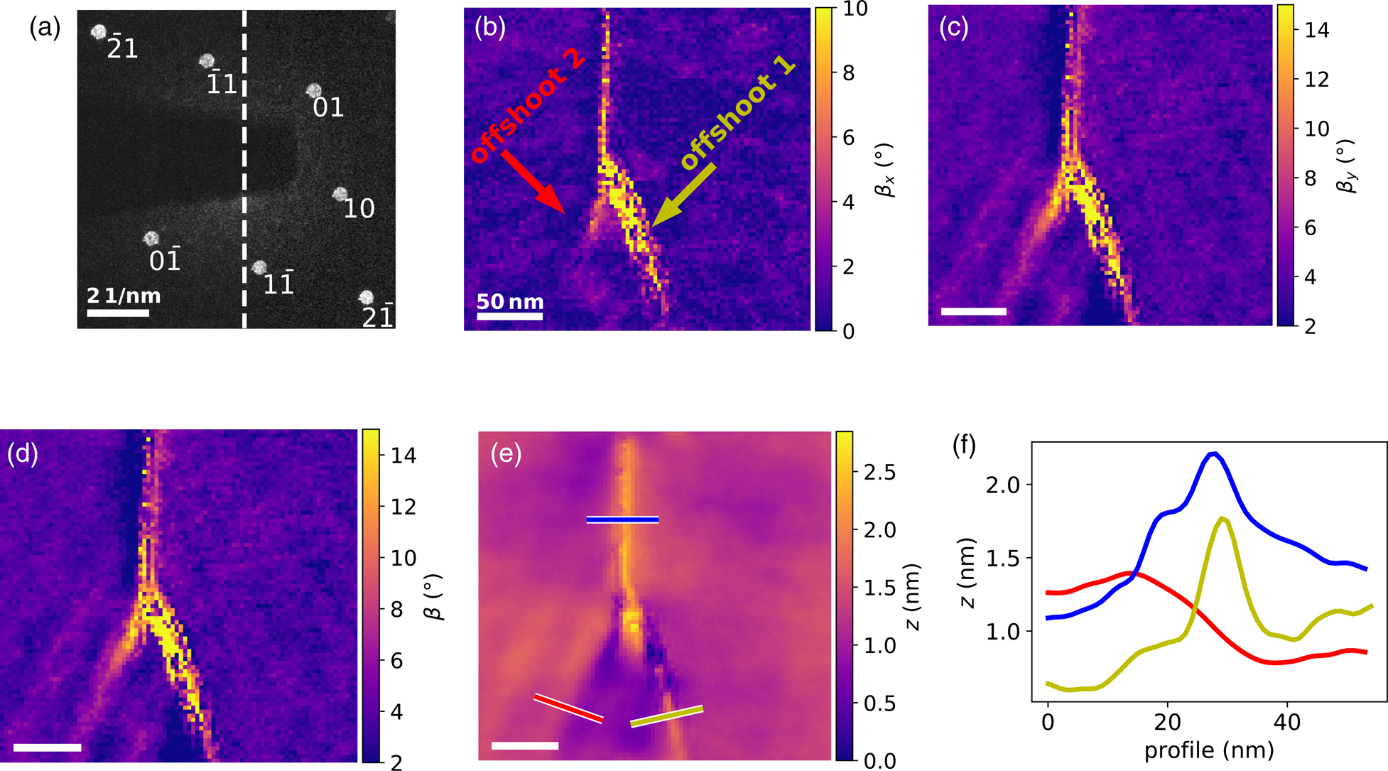
Fig. 8. Topography of the WSe2 monolayer, calculated by two NBED maps with α m = −2° and α p = 8° tilt. (a) NBED pattern including the diffraction spots used for the calculations. The dashed line indicates the tilting direction in diffraction space. The  $\bar {1}0$-spot is not visible here, because it is blocked by the beam stop. Absolute slope maps in the x- (b) and y-direction (c) and the total slope (d) in the region of the fold tip. The yellow and red arrows indicate the positions of the offshoot 1 and 2. (e) 2D representation of the height reconstruction of the slope maps. (f) Profiles of the fold (blue line) and the two offshoots along the lines marked in (e).
The influence of the topography is clearly visible when comparing the relative diffraction spot distances of the projected measurement (see Figs. 9d–9f) and the measurement accounting for the topography in Figures 9g–9i. The variations of lattice plane spacings in the three directions (a–c) indicate the biggest compression in the regions of the two offshoots in the case of the projection measurement. The slope in these regions, as shown in Figure 8, is comparatively high. The same region in (g–i) contains much higher values. The strain calculated from α m = −2° and α p = 8° suggests that the lowest values are between the offshoots. This would mean that the differences in lattice orientations between both sides of the fold are mostly compensated in the regions of the offshoots.
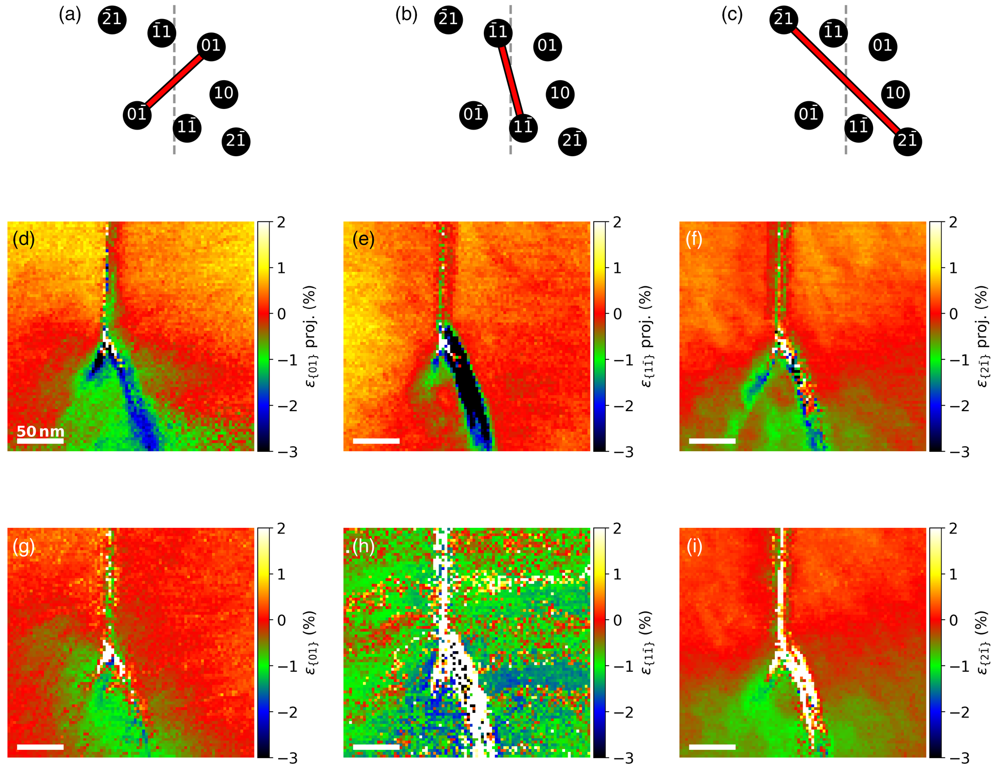
Fig. 9. Strain maps calculated using the relative distance of the diffraction spot pairs in (a–c). (d–f) Projected strain maps based on the NBED-map with α n = 0°. (g–i) Strain values adjusted for topographical effects based on the NBED-maps with α m = −2° and α p = 8° tilt. Since the  $1\bar {1}$- and $\bar {1}1$-spots are near the tilt axis, the noise level of (h) is relatively high.
The comparison of the angular lattice direction variations between the projection (shown in Figs. 10d–10f) and the topography corrected measurements, shown in Figures 10g–10i, reveal major discrepancies in the regions of the offshoots. This again indicates a significant influence of the topography at the projected measurements. Judging from the wide angular range of more than  ${\pm }5\percnt$ (~±7.5° (d), ~±4.4° (e), ~±6° (f)) it is likely that a large amount of the lattice rotation compensation between both sides of the fold is achieved by shear strain.
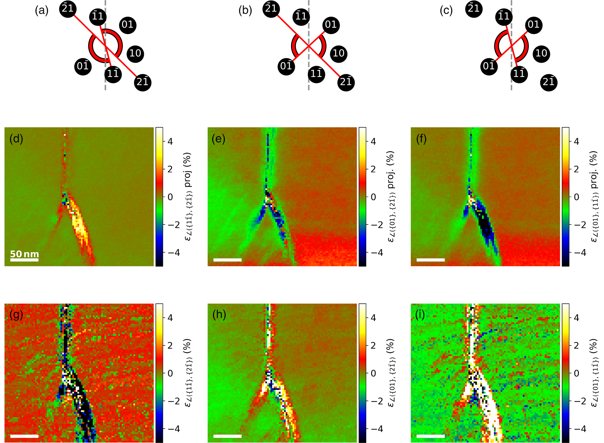
Fig. 10. Angular strain between the different lattice directions indicated with red-black lines in (a–c). (d–f) Projected angle variation maps based on the NBED-map with α n = 0°. (g–i) Angle variation calculated from NBED-maps tilted around α p = 8° and α m = −2°. Since the  $1\bar {1}$- and $\bar {1}1$-spots are near the tilting axis, the noise level of (g) and (i) is relatively high.
As expected, the largest discrepancies between the projected and the topography corrected measurements are in regions with large slopes.
Accuracy of the Technique
In the following, the main factors determining the accuracy of the method are discussed.
Influence of the Beam Limiting Aperture and Aberrations
For NBED, the electron probe typically has a diameter in the nm regime. If there is a structural transition in the 2D sample, due to strain or changes in the projected lattice spacings, halos around the corresponding diffraction spot are formed when the electron probe is at a position that lies between regions with different projected lattice spacings. This halo is caused by the beam limiting aperture, which is typically called the C2 aperture. The wave function at the back focal plane of the objective lens results from the diffraction pattern given by the propagation through the sample. Since the wave function at the C2 and the back focal plane are both in diffraction space, the shape of the diffraction discs corresponds to the shape of the C2 aperture. At the sample plane, the electron beam is ideally given by an Airy function. If for example part of the Airy disc is in a region of a compressed lattice, these electrons will be diffracted to higher frequencies in diffraction space. Higher frequencies can be found at the edges of the C2-aperture function, which leads to a diffraction disc with shifted edges. This phenomenon has already been analyzed for bulk crystals by Mahr et al. (Reference Mahr, Müller-Caspary, Grieb, Schowalter, Mehrtens, Krause, Zillmann and Rosenauer2015) at the interface of a GaAs–InGaAs heterostructure. A similar effect occurs in the intensity distribution of the direct beam when measured at space charge regions of p–n junctions (Clark et al., Reference Clark, Brown, Paganin, Morgan, Matsumoto, Shibata, Petersen and Findlay2018).
To emphasize how the C2 aperture influences the diffraction disc positions, a MoS2 monolayer with a Gaussian-shaped wrinkle along the  ${ 1\bar {1}}$-armchair direction was simulated, as shown in Figure 11e. At the transition between the flat and inclined region of the test structure, the halos can be seen particularly well at the (11)- and $( \bar {1}\bar {1})$-spots. The maxima of the cross correlation, which are used to determine the spot positions, are shifted, which is illustrated in Figures 11a,b and 11c,d. As a consequence, the variation of the spot position is often smaller than the actual projected strain. Figure 11f shows a comparison between the real strain and the strain measured from various diffraction spots during a scan across the test structure in {11}-direction. At the two positions −2.4 and 2.4 nm where the slope is the steepest, the absolute difference between εxx and the spot variations is largest. The strain values of the (11)-spot differs about 0.69 and 1.83%, the $( \bar {1}\bar {1})$-spot differs about 1.84 and 0.63% and the εxx strain in {11}-direction differs about 1.22 and 1.21% from the values of the projected strain.
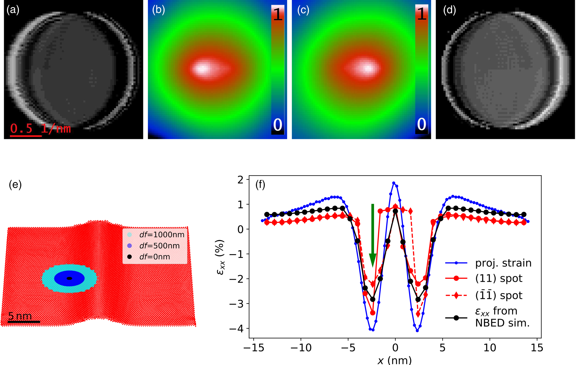
Fig. 11. Influence of the C2 aperture on the diffraction spot position using wrinkle 2 from Figure 2 as an example. The simulation settings for the NBED pattern are the same as the simulations before. (a,d) The (11)- and  $( \bar {1}\bar {1})$-diffraction spots at the position indicated by a black spot at the monolayer overview in (e). (b,c) The cross correlations of (a) and (d) with a template created from the central diffraction disc. The differently colored discs in (e) indicate the irradiated regions at different defocus settings, where the beam intensity is larger than 10% of the maximal beam intensity. (f) The strain across the wrinkle profile. The blue line is the relative position variations of the Mo atoms without the z-coordinate. The red and black curves are the relative diffraction spot variations of the (11)- and $( \bar {1}\bar {1})$-spots and the εxx- strain in {11}-direction using 16 diffraction spots from the 1, 2, and 3 order. The green arrow indicates the position of the diffraction spots shown in (a) and (d).
The same problem applies for the calculations of the slope maps and the height reconstruction as well.
Several different approaches have been proposed to determine the diffracted disk positions with high accuracy (Béché et al., Reference Béché, Rouvière, Clément and Hartmann2009; Müller et al., Reference Müller, Rosenauer, Schowalter, Zweck, Fritz and Volz2012; Mahr et al., Reference Mahr, Müller-Caspary, Grieb, Schowalter, Mehrtens, Krause, Zillmann and Rosenauer2015; Ozdol et al., Reference Ozdol, Gammer, Jin, Ercius, Ophus, Ciston and Minor2015; Pekin et al., Reference Pekin, Gammer, Ciston, Minor and Ophus2017; MacLaren et al., Reference MacLaren, Devine, Gergov, Paterson, Harikrishnan, Savitzky, Ophus, Yuan, Zuo, Forster, Kobe, Koppany, McClymont, Narendran and Riley2021). Therefore, we compared the applicability of the different techniques based on the simulated dataset. The standard registration technique, which was also employed in our work, involves cross-correlation with a template. Here, the intensity distribution in the correlation image directly relates to the intensity distribution of the diffracted spot making the result interpretable and robust against errors. However, cross-correlation tends to underestimate strain in case of a changing strain amplitude, because the peak in the correlation image broadens as it includes the signal of differently strained neighboring regions. In contrast to this approach, there is the possibility to employ edge-sensitive techniques, such as a combination of bandpass filtering with disk detection, gradient maximation or cross-correlation combined with Sobel filtering. These techniques resulted in noisy data and were not able to reproduce the expected features in the strain profile. This can be explained by multiple overlapping edges observable in the current dataset, leading to the detection of the different edge positions at random. Similarly, replacing cross-correlation by phase correlation resulted in highly scattered data, as this is again an edge-sensitive technique.
Therefore, it must be ensured that the probe size is smaller than the spatial extension of topographic variations. If this is not the case the diffraction space will contain many rods that are all oriented differently (Meyer et al., Reference Meyer, Geim, Katsnelson, Novoselov, Booth and Roth2007). For this reason, it is worth looking at the influence of aberrations which can be present at the scanning electron probe. Figures 12a and 12b show the influence of defocus (df) and threefold astigmatism (C23) on the probe size.Footnote 1 Using the test structure in Figure 11e, the tensile strain across the Gaussian wrinkle is simulated for different df- and C23-values (Figs. 12c and 12d). For df > 0.4 μm, the maximum at the center changes into an minimum. The flat parts of the test structure seem to dominate more with rising defocus values. In the case of higher C23-values, the course of the measured strain values become more asymmetric and shifts toward the right. This is caused by the orientation of the probe, which is no longer rotationally symmetric. Additionally, this aberration can lead to variations inside the diffraction discs intensities (Latychevskaia et al., Reference Latychevskaia, Woods, Wang, Holwill, Prestat, Haigh and Novoselov2019), which can also lead to shifts during cross-correlations.
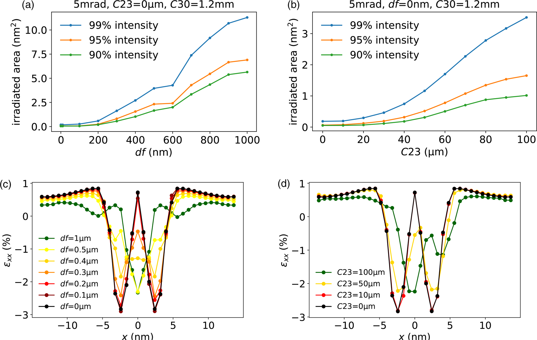
Fig. 12. Influence of the defocus and the threefold astigmatism on the electron probe size (a,b) and on the measured tensile strain (c,d). For better comparability, the simulation settings are the same as in the simulations before. The test structure used for calculating the strain is shown in Figure 11e.
Differences in the reconstruction in Figure 3 can be partly explained by the effects of the finite probe size, as well as the range differences between the theoretical strain values and the ones calculated from simulated NBED pattern in Figures 4–6.
It should be pointed out that despite the presence of double edges, due to the homogeneous inner contrast, the peak position is correctly measured by cross-correlation. Therefore, the strain variation is only affected by the probe size. Only if the probe size is larger than the spatial extension, the measurement starts to deviate.
Influence of the Tilt Angle
One of the main parameters when planning an experiment is the amount and direction of the tilt angles in order to be able to measure the topographical variations of interest. The tilt angle and direction must be chosen such that a large enough diffraction spot shift can be measured to calculate β. In Figure 13, the minimal tilt around the x-axis is shown, which makes the calculation of the slope of a diffraction rod in k x and k y-direction still possible. In this example, the first- and second-order lattice rod of a WSe2 monolayer is perpendicular to the tilting axis. If the rod position would lie close to the tilting axis, the minimum α x would be high, since otherwise the position of the intersection of the rod and the Ewald sphere would not change significantly. This is the reason for the high noise in Figures 9h, 10g, and 10i, where the  $( 1\bar {1})$- and $( \bar {1}1)$-diffraction spots are close to the tilting axis. The curves in Figure 13 are chosen to match the settings of the experimental data, with a first-order inverse lattice constant of 1/d {100} corresponding to (226.3 ± 0.6) pix.
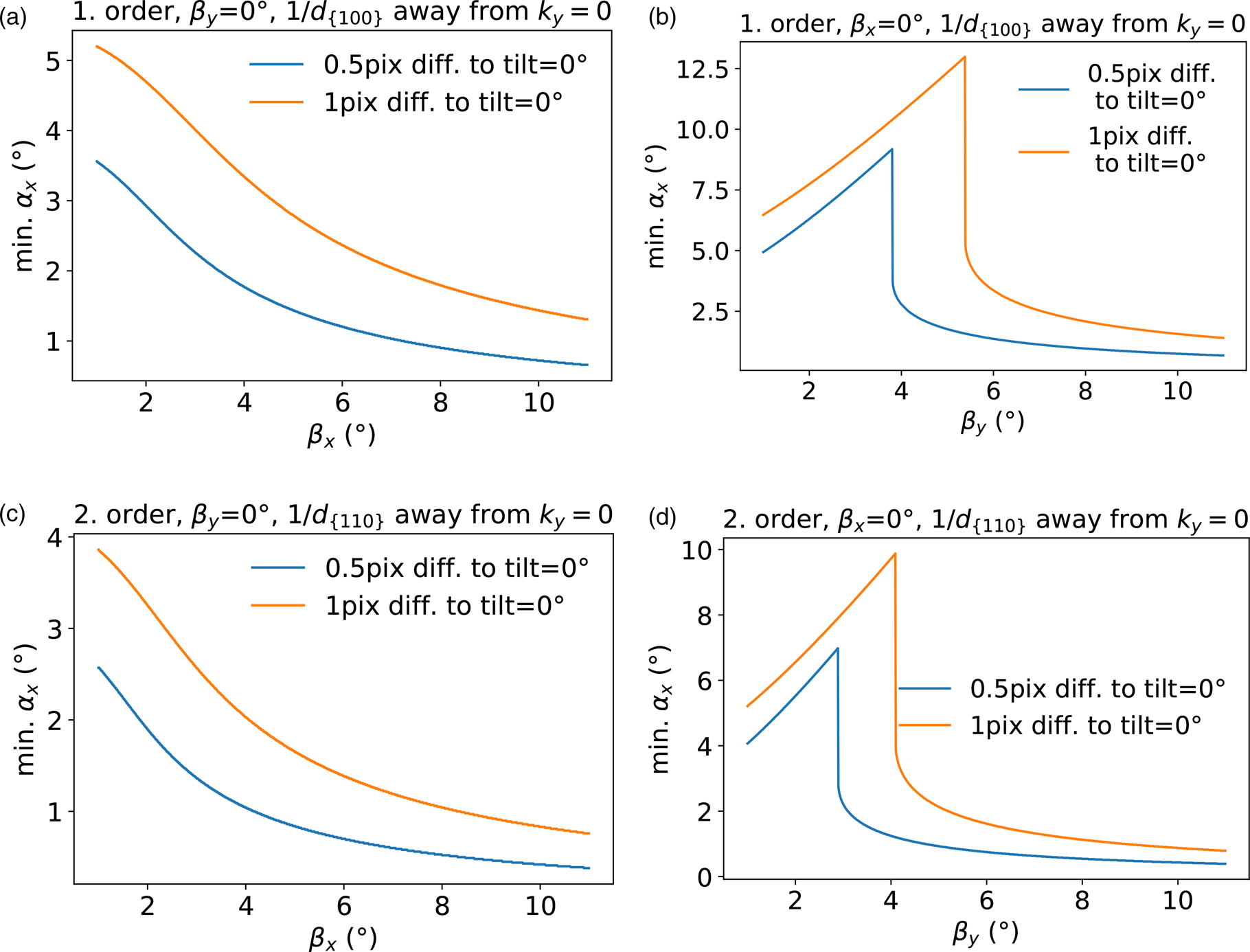
Fig. 13. Minimal tilt around the x-axis required in order to detect a certain slope of a first (a,b) and second (c,d) order reciprocal lattice rod in (a) and (c) k x or (b) and (d) k y direction, with an accuracy of 0.5 and 1 pixel. The curves are calculated using the settings of the experimental data.
Comparing a rod with a slope in the same direction as the tilting axis (see Figs. 13a and 13c) and perpendicular to the tilting axis (see Figs. 13b and 13d) for smaller slopes the detection accuracy will differ strongly. The impact can be observed in the underestimation of the slope of the Gaussian test structure introduced in the section “Extracting topography and strain information from simulated 2D samples” when only using the  $( \bar {1}1)$ diffraction spot and a tilt of α p/m = ±5° (see Fig. 14).
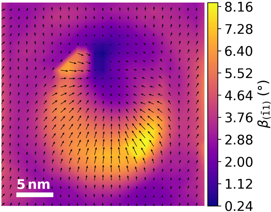
Fig. 14. Slope map of a Gaussian-shaped MoS2 monolayer calculated from two NBED-maps tilted around α = ±5°. The slope map was calculated only with the ( $\bar {1}1$) diffraction spot. The black arrows indicate the direction of the maximum slope at each pixel.
Taking into account the minimum required tilt angles, the significance of the topography measurement in Figure 8 can be further specified. Assuming a measurable difference of 0.5 pix (1 pix) the slopes detectable would be β x(0.5 pix) > 3° (β x(1 pix) > 4°) and β y(0.5 pix) > 3.8° (β y(1 pix) > 5.5°). The experimental data provided here should be understood as a first proof of principle. Further improvements can be made by choosing larger tilting angles.
To further improve the accuracy, additional maps with tilts in other directions could be recorded. The calculation of β x and β y would be overdetermined and residual errors would be smaller. The only disadvantages could be the increased radiation damage and more complicated location matching of all NBED-maps, as described in the following section.
Note also that the position mapping strongly depends on the intensity of the diffraction spots. The structure factor in k z-direction is modulated, depending on the material and the number of layers (Sung et al., Reference Sung, Schnitzer, Brown, Park and Hovden2019). Together with the influence of the Debye-Waller factor, this must be taken into account when designing an experiment. One could cool the sample to minimize thermal vibrations or to calculate the intensity distribution of the structure factor in advance to choose the tilt angles where the diffraction intensity is high.
Location Matching of Two NBED-Maps with Different Tilts
Changing the tilt of the sample can change the position of the sample slightly, even if the eucentric height is adjusted. For the calculations, both NBED maps need to be aligned. This is done by cross correlating the virtual bright-field images of both NBED maps and align them accordingly in real space. This leads to a correspondence of about 1 pix. With a pixel size of 3 nm, topographical changes in regions smaller than 6 nm are, therefore, hardly visible.
It is also advisable to tilt around the same amount in both directions, otherwise the projected pixel size will differ in the direction of tilt (|α p| = |α m|). In the experiment shown in this work, the effect amounts to 3 nm/pix · (cos( − 2°) − cos(8°)) = 0.01 nm/pix which was negligible.
Conclusion
We have demonstrated a procedure to distinguish between the local sample orientation and in-plane lattice strain of a 2D material. Taking advantage of the rod-like nature of the reciprocal lattice, the topography can be reconstructed from two NBED maps with different tilts. The theoretical concept of this technique was introduced, as well as a simulation and an experimental proof of principle. The topography of a simulated MoS2 monolayer could be reconstructed for a range of different probe sizes and tilting angles. Also, the tensile and the angular strain were calculated with deviations of less than 0.2% and 0.2° compared to the strain calculated from the atomic positions of the simulated test structure. Slope and height information of the WSe2 monolayer sample could be recovered. The mean height difference between the ground truth height and the recovered height information from the simulated NBED maps at tilt angles of α ± =20° is well below 0.06 nm.
Our method allows quantitative and independent measurements of strain and topography from the nm up to the μm-scale. Since only the rod-like nature of the reciprocal lattice is required, this method should be applicable for all 2D structures with weakly modulated structure factors. Contrary to other methods (Segawa et al., Reference Segawa, Yamazaki, Yamasaki and Gohara2021; Xie & Oshima, Reference Xie and Oshima2021), our procedure does not require any detailed knowledge of the specimen structure. For this reason, we like to point out that the proposed method could, in principle, also be used for more complex structures such as multilayer samples (Sung et al., Reference Sung, Schnitzer, Brown, Park and Hovden2019), heterostructures consisting of different monolayers (Han et al., Reference Han, Nguyen, Cao, Cueva, Xie, Tate, Purohit, Gruner, Park and Muller2018; Latychevskaia et al., Reference Latychevskaia, Woods, Wang, Holwill, Prestat, Haigh and Novoselov2018), or monolayers sandwiched between or on top of a thicker substrate (Thomsen et al., Reference Thomsen, Gunst, Gregersen, Gammelgaard, Jessen, Mackenzie, Watanabe, Taniguchi, Bøggild and Booth2017), as long as the diffraction spots of the layers in question can be isolated from diffraction spots of the other components of the sample.
Acknowledgments
We thank Martin Peterlechner and Sven Hilke for fruitful discussions and help with the experimental setup, Robert Schneider and Iris Niehues for help with sample preparation, and Christian Schwermann for an introduction into molecular dynamics simulations.
We acknowledge support from the Open Access Publication Fund of the University of Muenster.


 Open access