


Introduction
The silicon-based energy-dispersive spectrometer (EDS), which can produce an entire X-ray spectrum without moving parts, has been serving microanalysis for over 50 years. But in 1984, based on the work of Gatti and Rehak [Reference Gatti and Rehak1], development of a new type of EDS detector that could collect X-ray photons 100 times faster than previous semiconductor devices began. In fact, over the last decade, the silicon drift detector (SDD) has completely superseded the previous EDS technology in every important performance parameter.
A semiconductor-based EDS was first applied to X-ray microanalysis in 1968 by attaching a 3 mm-thick Si(Li) detecting crystal to the column of an electron probe microanalyzer (EPMA) [Reference Fitzgerald2]. At that time, the reigning method for measuring X-rays in electron-beam instruments was the crystal spectrometer that produced peaks about 10 eV wide compared to 600 eV wide for early Si(Li) detectors. Even so, the EDS became popular because most elements (Z = 11 to 92) could be detected in 5 minutes, compared to scanning four separate crystals for 30 minutes to detect the elements present in the specimen. Also, since there was considerable freedom in locating the EDS detector within the specimen chamber, the Si(Li) device was quickly adapted to the scanning electron microscope (SEM).
The mechanism for detecting X-rays in a Si-based detector is straightforward in principle. An X-ray entering the active or sensitive region of the detector creates a number of electron-hole pairs proportional to the energy of the incoming photon. In the case of the SDDs the electrons are collected at the readout node while the holes are absorbed in the rectifying p+ contact. The pair creation energy w in silicon is about 3.68 eV at room temperature. This means an X-ray photon of 1 keV produces on average 272 signal electrons. By measuring this small amount of charge, the detector determines the energy of each individual photon as it contributes to the X-ray spectrum. The initial mating of the old Si(Li) detector with the SEM and the transmission electron microscope (TEM) was a successful marriage for over three decades. In that time the energy resolution (peak width) of this device improved from 600 eV to 130 eV, but there were significant drawbacks. X-ray photon counting was rather slow at good energy resolutions, typically only 3000 counts per second (cps), which forced long collection times to obtain a precise quantitative analysis and hours-long acquisition times for quality compositional images (X-ray element maps). There was also the inconvenience of cooling the Si(Li) crystal and its field effect transistor (FET) amplifier to near liquid nitrogen temperatures to reduce noise in the signal.
About two decades ago an EDS detector system containing a new sensor based on the novel SDD technology became available [3]. These SDD sensors were fabricated by a team in Munich [Reference Lechner4], which was dedicated to development of detectors for space research. They adopted the lithographic techniques and planar technology of the microelectronics industry for detector fabrication. However, to realize the concept of sideward depletion, an important modification was introduced: the double-sided processing of silicon wafers. The SDD overcame the difficulties present with Si(Li) detectors. Recent SDDs with thermoelectric cooling to -20°C collect X-rays at least two orders of magnitude faster, at slightly better energy resolution, and without the need for liquid nitrogen cooling.
Today all high-resolution commercial X-ray spectrometers employ some variation of the SDD. SDDs are used in more than 300,000 instruments for science and industry to detect particles, X-rays, and scintillation light. Some of the many applications of SDDs are as tracking detectors in high-energy physics experiments, as electron spectrometers in neutrino experiments, as X-ray spectrometers for astronomy, as light detectors coupled to scintillators, as high-speed X-ray spectrometers in X-ray fluorescence units, and in microanalysis systems for electron microscopy [Reference Guazzoni5]. This overview will concentrate on the development of SDD spectrometers for X-ray microanalysis in electron microscopes, including the latest achievements in terms of energy resolution and count rate capability.
The Physical Concept of SDDs
Early work and the concept of sideward depletion
Since their invention in 1983 [Reference Gatti and Rehak1], SDDs have left deep traces in the field of radiation detection. Emilio Gatti (1926–2016), a frequent visitor at Brookhaven National Laboratory (BNL), and Pavel Rehak (1945–2009), a scientist at BNL, discussed the topic of how to move the signal electrons generated in a fully depleted silicon crystal to a point-like, low-capacitance readout node.
In 1969, Boyle and Smith invented the charge coupled device (CCD) [Reference Boyle and Smith6] for imaging and signal processing purposes. The transfer of signal charges in a CCD was performed by rapidly changing voltages of isolated shift electrodes on the surface of the CCD to create time-variant potential wells inside the semiconductor. In contrast to this approach, Rehak and Gatti were exploring a constant drift field such that the detector could be operated in DC mode without changing voltages. Therefore, Rehak called the SDD a phase-less CCD or a pnCCD, a discretely transferring SDD, to highlight the similarities and differences of the two devices.
A double-sided polished high-resistivity n-type silicon wafer can be entirely depleted of mobile charge carriers if both wafer surfaces are covered with rectifying p+ junctions (Figure 1a). Only a very small ohmic n+ contact is needed to apply reverse bias voltages and drain off all mobile charge carriers. With proper bias voltages the depletion occurs from both wafer surfaces until the detector volume is completely sensitive. The small ohmic n+ node is then the most positive point in the detector structure where all the signal electrons will be collected (Figure 1b). As this node can be made geometrically very small, its capacitance with respect to all other contact becomes small as well. The collected signal electrons generate a voltage swing ΔV at the collecting node that is proportional to the number of collected electrons according to ΔV = ΔQ/C (ΔV is the voltage swing, ΔQ the amount of charge, and C the total node capacitance). For example, a 40 fF node capacitance yields a voltage change of 4 μV for every collected electron.
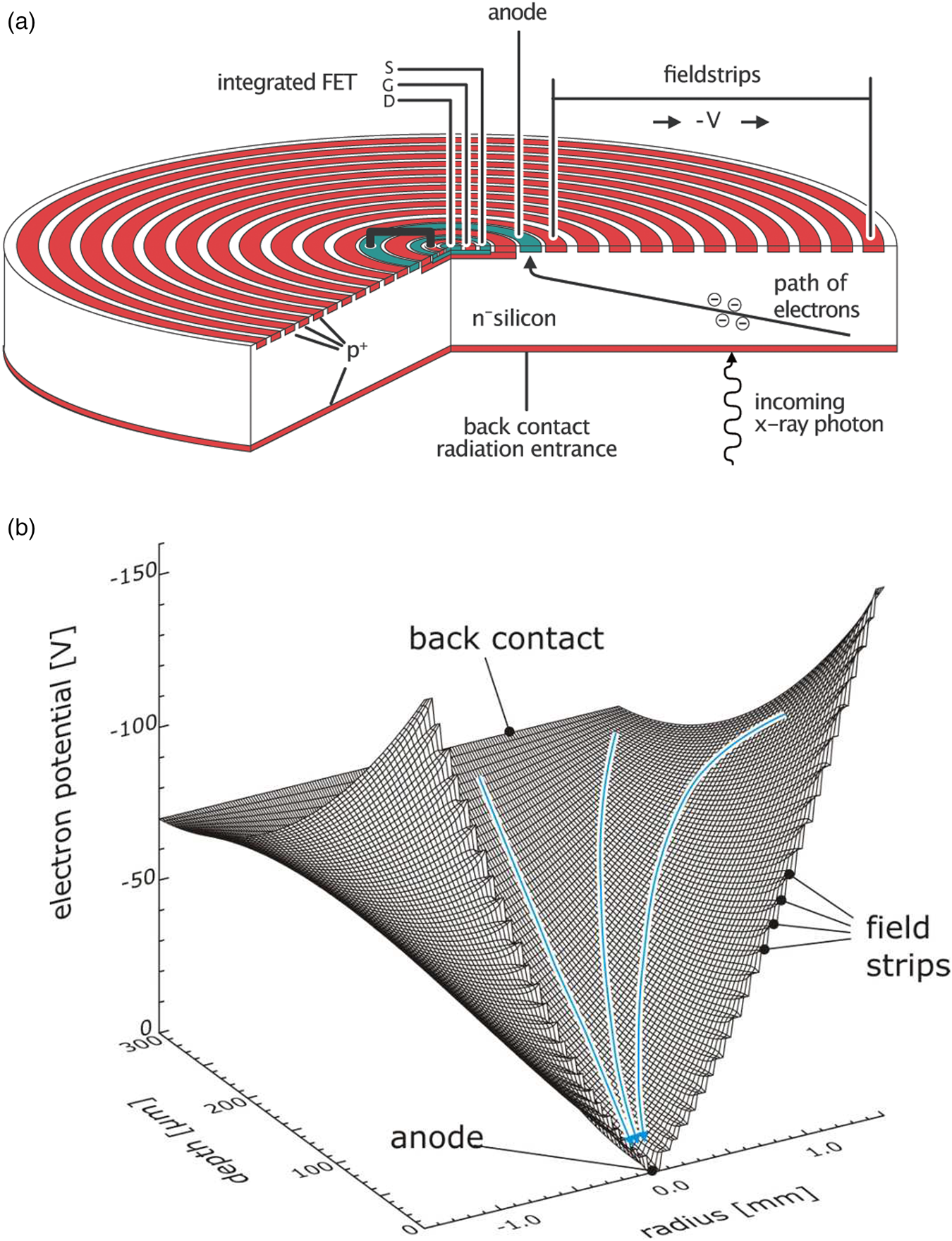
Figure 1: (a) Cross section of a cylindrical SDD with an integrated single-sided n-channel JFET. The green ring in the center represents the signal-electron collecting anode, and the red rings are the p+ drift rings (field strips), producing a graded electric field that forces the signal-electrons to the read node. The homogeneous radiation entrance window is at the back of the device where the p+ back contact can be seen. (b) The electron potential is shown with the field strips, the equipotential on the back contact, and the collecting node at the radial position 0.0. Once electrons are generated in the SDD volume, they experience at every point an electrical field component that drifts them toward the anode.
As can be seen from equation (1) the noise, or more accurately the equivalent noise charge ENC, expresses the influence of various physical noise sources on the total noise of a detector readout as a function of detector and transistor parameters. It can be understood as the number of fluctuating electrons that must be injected into the input of the amplifier to generate the measured total noise at the output.
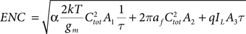 $$\;ENC\;\; = \;\sqrt {\alpha \displaystyle{{2kT} \over {g_m}}C_{tot}^2 A_1\displaystyle{1 \over \tau} \; + \;2\pi a_fC_{tot}^2 A_2\; + \;qI_LA_3\tau} \;$$
 In equation (1) k is the Boltzmann constant; T is the temperature; α is a parameter describing the input noise source; gm is the transconductance of the first transistor; A 1, A 2, and A 3 are constants describing the frequency-depending filtering; af parameterizes the so-called “low frequency noise”; q is the elementary charge; and IL is a DC electron current, for example, the thermally generated leakage current or dark current. The first term under the square root is called the series noise and scales with  $C_{tot}^2 $ and $\displaystyle{1 \over \tau} $. That means if the total input capacitance is large, the series noise increases. For a given capacitance C, the noise contribution can be reduced only by extending the signal processing time τ, with the consequence of reading out the signals at a low rate, or by increasing gm of the first transistor. The second term is independent of the signal processing time τ, but again this is proportional to the total input capacitance $C_{tot}^2 $. This contribution is called low frequency noise. Both components, the series noise and the low frequency noise, heavily profit from a low input capacitance. The last term is independent of the total input capacitance but proportional to the signal processing time τ. This depends on the thermally generated leakage current or dark current and can be controlled by an appropriate operating temperature and an optimized sensor fabrication technology. To summarize: if you want to readout fast at a low noise, the total input capacitance must be minimized. To obtain the system energy resolution, the noise contribution from equation (1) has to be quadratically added to the Fano noise (equation 2) caused by statistical fluctuations of the ionizing process:
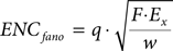 $$ENC_{fano} = q\; \cdot \sqrt {\displaystyle{{F\cdot E_x} \over w}} \;$$
where F is the Fano factor in silicon (F = 0.115), Ex is the X-ray energy, and w is the pair creation energy. The Fano contribution to the full width at half maximum (FWHM) describes the theoretically achievable lower limit of the energy resolution. More details about the physics of SDDs can be found in [Reference Lechner4,Reference Lutz7].
First commercial SDDs
The very first mention of SDDs as new and compact Peltier-cooled X-ray spectrometers was in 1995 [Reference Strüder and Soltau8]. The SDD chips were developed and fabricated at the semiconductor laboratory of the Max Planck Institute for Extraterrestrial Physics in Munich. The first commercially available SDD detector systems were offered by Röntec, now Bruker Nano, in 1997 for element mapping applications [Reference Fiorini9,Reference Strüder10] with SDD chips delivered from the Munich team. The XFLASH system from Röntec produced count rates that were 10×–100× higher than Si(Li) systems, and the thermoelectric cooler kept the detector at -30°C without liquid nitrogen [3,Reference Lechner4]. This allowed detailed element distribution maps to be acquired in a few minutes versus several hours. But at this time, for serious X-ray spectrometry requiring good energy resolution, excellent low-energy X-ray detection, good peak-to-background (P/B) performance, and reliable background measurements, a Si(Li) detector was still needed in addition to the SDD employed for X-ray mapping. Several years of continuous improvements in device fabrication and pulse-handling electronics followed, resulting in the production of an SDD system that counts remarkably fast, while at the same time providing excellent energy resolution on peaks. This allowed overlapping lines to be separated better than previously possible with the Si(Li) detector. The following sections tell the story of these improvements.
Performance Improvements of SDDs
Figures of merit
Typical figures of merit for the qualification of SDDs are the same as for Si(Li) detectors: (a) energy resolution at the 5.898 keV manganese Kα line from an 55Fe radioactive source, (b) the P/B ratio at Mn Kα, (c) energy resolution at the 277 eV carbon Kα line, (d) count rate capability and energy resolution at various processing times, and (e) stability and reproducibility. These parameters are important for electron beam microanalysis (in SEMs and TEMs) and for X-ray fluorescence analysis [Reference Newbury and Ritchie11]. For these analytical techniques, beyond a high count rate capability, an X-ray spectrometer should produce narrow peaks (good energy resolution) to separate peaks from different elements and a high P/B to detect small amounts of elements. For use in electron microscopy the solid angle value, low X-ray background, and cost are also important issues.
Detector shape with FET integration
Figure 1 shows what came to be the SDD configuration commonly employed in microanalysis for detecting X-rays with energies from 30 eV up to 30 keV. The traditional SDD for microanalysis has a cylindrical shape with an integrated n-channel junction field-effect transistor (JFET) in the center to minimize read node capacitance. Field strips (drift rings) produce a graded electric field that forces signal electrons to drift toward the anode. Once the staircase of collected signal charges at the charge-sensitive amplifier output reaches its limit, a reset mechanism allows the process to repeat. Integration of the transistor in the SDD reduced the total input capacitance dramatically, thus reducing the electronic noise and increasing the speed of signal processing. This configuration eliminates microphonic effects and delivers an on-chip-at-low-impedance signal to the next amplification stage. The cylindrical shape of this type of SDD allows for an optimal signal charge collection speed.
SDD sizes and arrays
The low capacitance of these detectors allowed large sensitive areas, as well as detector arrays where X-ray detection can be combined from several individual channels, to further increase the count-rate capability by increasing the field of view. A large number of SDD variations have been derived from this basic concept (Figure 2): large-area oval-shaped detectors with sensitive areas from 5 mm2 up to 200 mm2, hexagonally shaped arrays of SDDs, a droplet-shaped configuration for capacitance minimization [Reference Soltau12], and SDDs with integrated FETs and external FETs. A design particularly useful for the SEM is a circular array of four SDDs around a central hole, which brings the detectors as close as possible to the specimen, providing the maximum solid angle for X-ray collection (Figure 3).
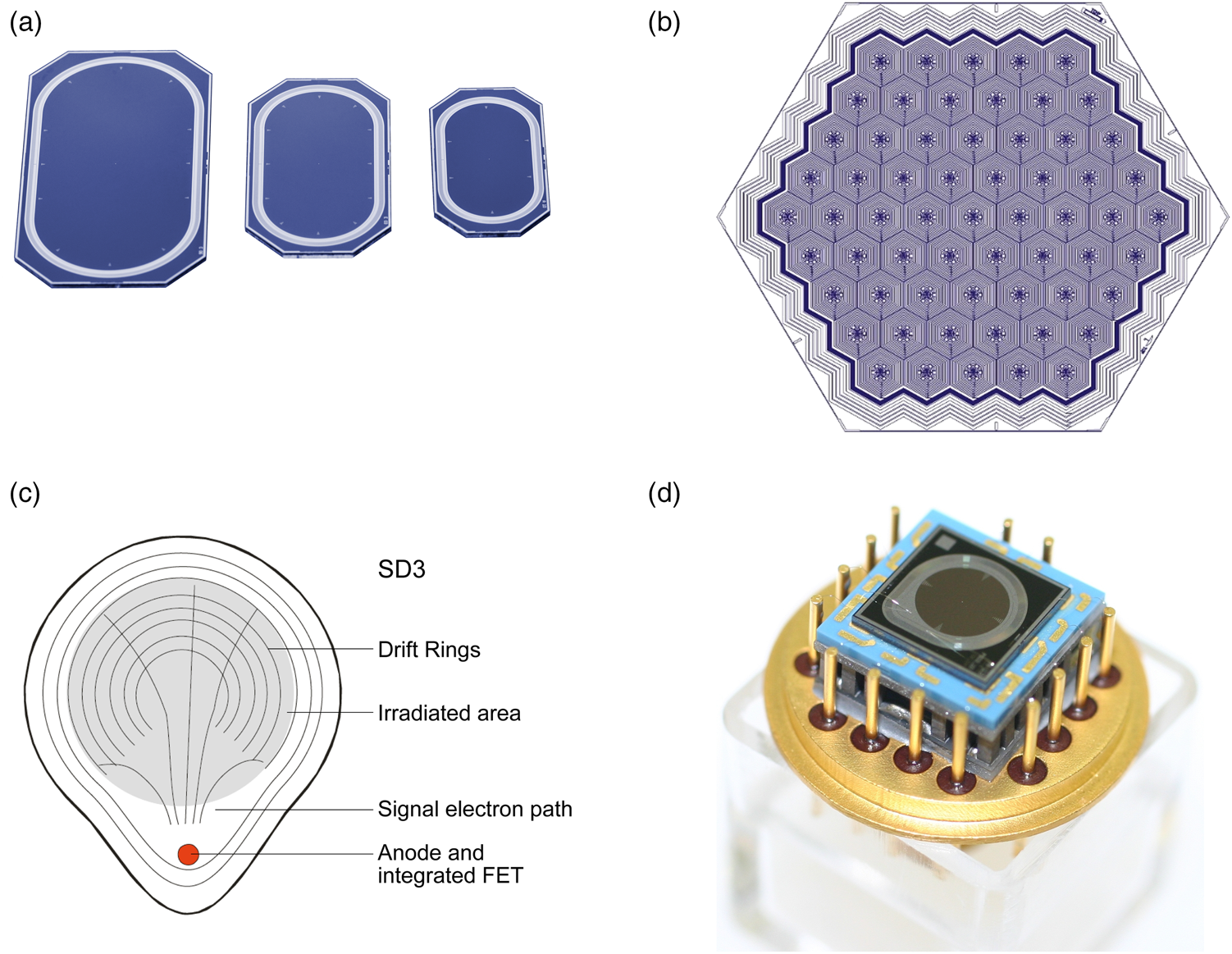
Figure 2: Examples of SDD geometries. Beyond the classical round or square-shaped SDDs, oval and droplet shapes have been realized, as well as a variety of arrays built to increase the effective sensitive area and the field of view. (a) Large-area large area oval-shaped detectors with sensitive areas from 5 mm2 up to 200 mm2, (b) hexagonal array comprised of a 61-channel SDD with a total area of more than 3 cm2, (c) the tear-drop detector shaped array designed to reduce capacitance has an internal FET located outside the irradiated area, (d) tear-drop detector mounted on a ceramic substrate, which is coupled to a Peltier cooler underneath. The 16 metal pins surrounding the ceramic and Peltier element serve as electrical connections to the outside of the TO-8 housing, the bottom part of which is shown in gold color.. The cover with the external entrance window is not shown.
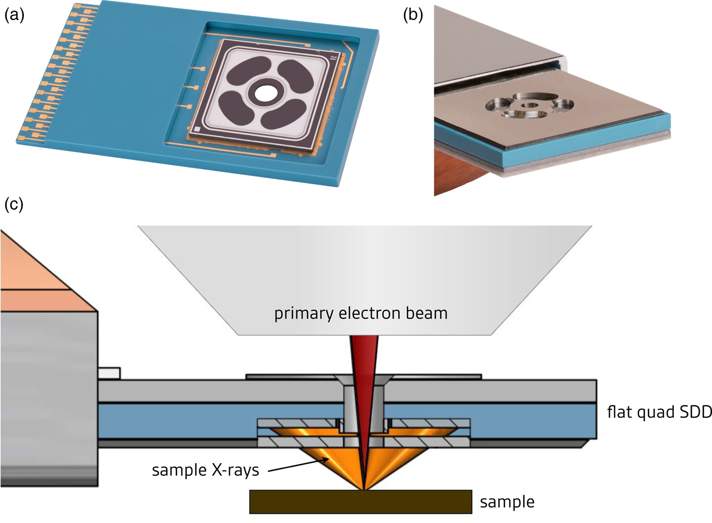
Figure 3: A flat four-channel detector for an SEM. (a) Plan-view of four kidney-shaped sensors around a center hole, (b) perspective view, (c) four-channel detector mounted between the SEM final lens and the sample. This configuration provides a high solid angle (up to 1.5 sr) for a detector with a total count rate capability of 6 × 10⁶ counts per second.
Energy resolution and P/B
Energy resolution is defined as the FWHM intensity of the 5.898 keV Mn Kα line measured at a low counting rate of 1000 to 3000 cps. This specification is a leftover from the old Si(Li) times where good energy resolution was only achieved at long signal shaping times τ and consequently low count rates. For SDDs this limitation in count rate is no longer required. For example, the energy resolution of an early cylindrical SDD in 1996 of 3.5 mm2 active area, measured at room temperature with a shaping time of 500 ns, was 225 eV (FWHM) at 5000 cps. When the same SDD was cooled with a thermoelectric cooler (TEC) to approximately -20°C and measured with a processing time of 2 μs, it had an energy resolution of 152 eV (FWHM) at 5000 cps [Reference Boyle and Smith6].
The P/B ratio for the present work is defined as the maximum number of counts in the signal peak of the 5898 eV Mn Kα line divided by the mean value of counts in the energy range from 900 eV to 1100 eV. For early SDDs described above at -20°C, the P/B was 3000:1. While not fully satisfactory, this experimental detector was a good starting point. Today the P/B is typically between 15000:1 and 20000:1. It mainly depends on the total noise and the quality of the internal radiation entrance window.
The energy resolution of the above mentioned early SDDs that were in use around 1996 was not fully satisfactory in comparison with the conventional Si(Li). In a first development step the electronic noise was lowered from approximately 10 electrons (rms) [Reference Lechner4] achieving an energy resolution of 152 eV at Mn Kα, with a 3.5 mm2 small SDD operated at -20°C, to less than 5 electrons (rms) in 2008 at 100,000 counts per second for a 10 mm2 active area. The C Kα peak could not yet be properly detected in the late 90s.
In 2008 [Reference Soltau13] the FWHM of the Mn Kα line was already reduced to 124 eV for a 10 mm2 large detector with a P/B above 15000:1 [Reference Soltau13]. The best guaranteed values today are 121 eV at shaping times τ around 1 μs allowing for very high count rates and a P/B beyond 15000:1. The latter values are already very close to the theoretically achievable energy resolution given by the Fano ionization statistics, which is 119 eV at 5.9 keV. The total electronic noise is 2 electrons (rms) due to the reduction of input capacitance to less than 50 fF—the key to obtaining excellent spectral performance and count rate capability [Reference Niculae14].
Low-energy X-ray detection
Starting in 2007 the proper detection of B (at 180 eV) became achievable [Reference Newbury and Ritchie11]. At this time C Kα could be measured with a resolution of 42 eV (FWHM). A precondition to enter that energy domain was the very low noise of the detector system, but that was not sufficient by far. The X-ray attenuation length is about 100 nm at 300 eV. As there are typically several tens of nm of layers covering the rectifying p+ implant for passivation reasons, a fraction of the incoming radiation is absorbed in these layers before entering the highly doped reverse-biased p+ diode. This highly doped region has undergone radiation damage during the implantation process. The subsequent annealing repairs and activates the disturbed silicon lattice as much as possible. The interaction of the low-energy X-rays in these layers results in partial signal collection leading to a decreased energy resolution.
At carbon K (277 eV) the theoretical limit of Fano noise originating from ionization statistics is 26 eV (FWHM). The measured width is the result of the Fano and electronic noise on one side, but a certain fraction is also due to partial signal electron loss in the internal radiation entrance window. Thus, the problem of not reaching the Fano-limited energy resolution at X-ray energies below 500 eV is related to the quality of the radiation entrance window. Because the physics and the technology of the X-ray entrance window became better understood and then implemented in the fabrication process, the energy resolution at the 277 eV carbon K peak improved from 85 eV at the beginning of development in 2004 to 35 eV by 2019 [Reference Niculae14], while at the same time the P/B ratio at the Mn Kα line went up from 3000:1 to more than 15000:1 (Figure 4). At that point, X-ray lines for light elements down to Li (54 eV) could be clearly detected (Figure 5).
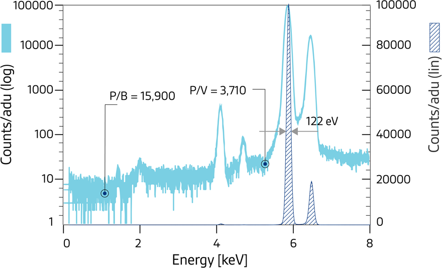
Figure 4: Energy spectrum of emissions from a 55Fe source. The measured energy resolution is 122 eV (FWHM) at the Mn Kα line (5898 eV), and the P/B ratio is 15900:1. The silicon escape peaks from the Kα and Kβ lines at 4.15 keV and 4.75 keV are clearly visible. The other features at 1.49 keV and 2.0 keV are fluorescence lines from Al-K and Zr-L lines, materials used in the experimental setup. The Y-axis shows the number of counts per analog-to-digital units (adu), that is, the number of counts per ADC bin on a logarithmic (left) and a linear scale (right).
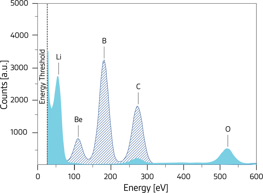
Figure 5: Composite low-energy spectra measured with a droplet SDD. The fully blue spectrum was taken from a pure Li sample partially oxidized; the shaded spectrum is from a commercially available radiation entrance window made of beryllium and coated with boron hydrate. The carbon peak in both spectra originates from the glue and carbon contamination in the SEM. The 4σ event threshold was set to 25 eV, corresponding to a system noise of less than 1.8 electrons (rms). The Li-K line at 54 eV (14 electron hole pairs created) is clearly separated from the noise. The measured FWHM of B-K at 183 eV is 32 eV, and the width of C-K is 36 eV.
Long-term stability and reproducibility
Under heavy irradiation of X-rays and electrons, the energy resolution can deteriorate. Two major contributions are well known: (1) degradation of the internal radiation entrance window and (2) the increase of dark current. One sensitive way of quantifying these effects is the onset of increased FWHM in the Mn K line at 5.9 keV. By irradiating the SDD with photons from a Mo X-ray tube with its prominent 17.35 keV Kα line and strong bremsstrahlung continuum or from a radioactive 55Fe source, degradation effects can be studied. Typically, 1014 X-rays can impinge on the detector before the widening of the Mn Kα line is detected. This corresponds to a continuous operation for 10 years with 350,000 cps. By studying the spectra as a function of the signal processing time, the P/B ratio, and the response to low-energy X-rays, the damaging mechanisms can be analyzed.
Count rate capability
The next performance parameter that improved in the past 10 years was the readout speed—the number of X-ray photons per second the readout node can process and convert into digital units (X-ray photon counts as a function of energy). From the interaction point of the incoming X-ray with the silicon lattice, the generated signal charges (electrons) must be forced to drift to the collecting read node. During the drift phase they experience diffusion and electrostatic repulsion in the drift direction at the bottom of the potential parabola (Figure 1b).
The upper limit of the count rate is governed by two factors: the speed of the signal electrons along the drift direction and the speed of the processing electronics. The former is mainly determined by the effective electric field, the saturation velocity, the drift distance, and the temperature; while the latter depends on the total input capacitance, the transconductance of the first FET, and the device temperature.
With drift fields of the order of 500 V/cm, drift velocities of 10 μm/ns are attainable at -20°C. This translates in a time distribution spread of signal charge arrival at the collecting node of approximately 30 ns (rms) after a drift length of 3 mm. This leads to a rise time of the first amplifier of approximately 50 ns, taking into account the capacitance of the read node and the properties of the first amplifying FET.
If the signal processing time of the amplifier is shorter than the spread of the arrival times of the signal charges, not all electrons reach the read node during the shaping time τ of the amplifying system. In this case a ballistic deficit occurs. As a consequence, the amplitude measurement is degraded, and the energy resolution deteriorates. Therefore, special attention is dedicated to fabricating the p+ drift rings that generate the electric field such that the drift of the signal charges gets as close as possible to the electron saturation velocity in silicon. In addition, the ballistic deficit problem can be partially mitigated by using modern digital pulse processors.
Both a short collection time of the signal electrons and a low total capacitance of the input node lead to further improvements of the energy resolution at very short signal processing times. Figure 6 shows that even at an analog shaping time of 125 ns, the energy resolution for the most recent generation of SDDs was below 127 eV with a signal rise time shorter than 50 ns. The count rate capability of current SDDs recorded with a standard digital pulse processor (DPP) can be nearly 600,000 output counts per second for an incoming count rate of 1.45 × 10⁶ counts/second (Figure 7). More sophisticated DPPs may increase the above count rate by another factor of two, still maintaining an energy resolution of 145 eV (FWHM). To achieve good energy resolution at even higher count rates, the detector active area can be increased by combining the signals from several medium-sized multichannel SDDs (Figure 2) to reduce the ballistic deficit effect described above.
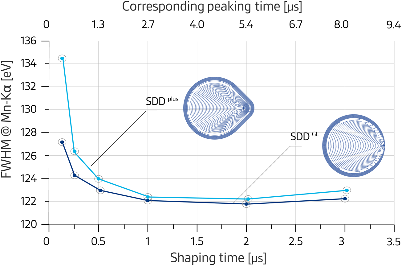
Figure 6: Energy resolution as a function of the signal shaping time (τ, see text above) and peaking time (time when the pulse reaches the maximum: here: 2.7 × τ) for two different detector designs. The data were taken with an analog shaper. It shows that a 127 eV energy resolution (FWHM) can be obtained with a signal shaping time of 125 ns at – 20°C. Both measurements were performed at 15000 cps. The short shaping time allows for room-temperature operation with an energy resolution of 135 eV (FWHM).
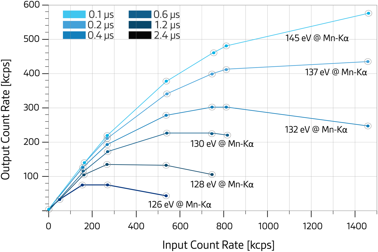
Figure 7: Output count rate versus input count rate as a function of the processing time for each entering X-ray photon recorded with a standard DPP. As the processing time decreases, the energy resolution on the Mn-Kα peak decreases as well. Thus, 1.5 × 10⁶ incoming X-rays per second can be detected with an energy resolution of 145 eV, leading to an output count rate into the spectrum of almost 6 × 10⁵ counts/second per SDD channel. At the other extreme, for an energy resolution of 126 eV the output count rate can be 70000 cps.
Quantum efficiency
A high quantum efficiency (QE) over the full energy range from 50 eV to 30 keV is required to satisfy the need for a high number of recorded X-ray photons in a short measurement time. In the case of energies below 2 keV, operation in vacuum is mandatory. In this case “windowless” SDDs are usually used. The internal radiation entrance window of the sensor is often a combination of a highly doped rectifying p+n junction, thin dielectric films, and possibly a visible-light-absorbing aluminum layer. The low-energy side of the QE curve in Figure 8 is dominated by signal losses at the internal radiation entrance window of the SDD sensor. In the case of a non-controlled environment, SDDs are encapsulated in a TO-8 housing, and an additional external radiation entrance window is implemented, strong enough to withstand atmospheric pressure and to ensure a local vacuum around the SDD. Recent external windows are constructed from thin Si3N4 and SiO2 layers supported by a Si grid, which blocks only about 25% of the entering X-rays at 800 eV. As in the case of the internal radiation entrance window of the sensor, a thin layer of aluminum is often deposited on the outer surface of the external radiation entrance window to minimize detection of visible light (from cathodoluminescence) and infra-red (from chamber components). In the case of the internal radiation entrance window without the light-blocking aluminum, the black curve in Figure 8 had a quantum efficiency that was always above 85% (0.85) for X-ray energies between 500 eV and 11 keV for a 450 μm thick detector. The drop in efficiency above 10 keV is due to the rapid decline in the cross section for the photoelectric processes in silicon, allowing many incoming high-energy X-rays to pass through the detector without being absorbed. The blue and red curves show the QE with 50 nm and 150 nm Al on top of the internal radiation entrance window to block the visible light. Even for incoming X-rays of 25 keV, the QE is still 20% (0.2). To increase the sensitivity for X-ray energies up to several hundred keV, a scintillator can be combined with an SDD as a photo detector to measure the scintillation light of the converted gamma rays with energies up to more than 1000 keV [Reference Fiorini15].
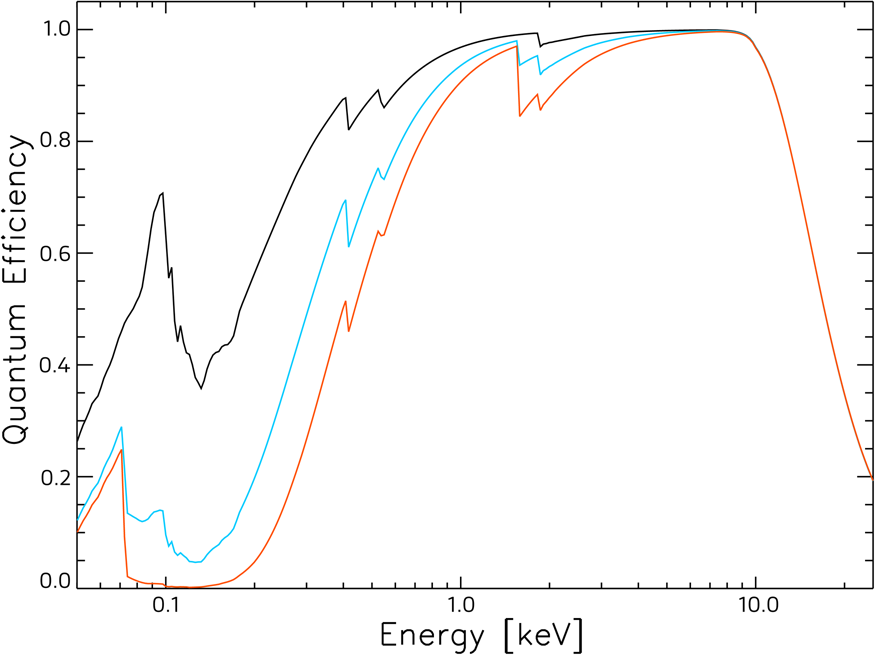
Figure 8: Quantum efficiency of a 450 μm thick silicon detector as a function of X-ray energy from 50 eV to 25 keV. In this special case, the quantum efficiency of the internal X-ray entrance window composed of dielectric layers is shown along with two thicknesses of aluminum as a visible light absorber. The black curve shows the QE without aluminum. The blue curve is for an Al layer of 50 nm, which attenuates visible light by a factor of 103. The red curve shows the effect of 150 nm of Al to block the visible light by more than a factor of 106. Note that for the red curve the detector can collect some Li photons at 54 eV, but no Be (109 eV) or B (183 eV) photons.
The efficiency shown in Figure 8 is sufficient for most microanalysis tasks because all elements heavier than helium emit K-, L-, or M-shell photons in the range 50 eV to 10 keV. The figure also shows that a 50 nm Al layer (blue line) allows the detection of Li X-rays at 54 eV, Be at 109 eV, B at 183 eV, and C at 277 eV. A 150 nm (red line) Al layer absorbs nearly all X-rays from Be and B.
Practical Considerations
Thermoelectric cooling
The detector operational temperature range is typically from -70°C (for microanalysis requiring the best energy resolution) up to +40°C (for handheld X-ray fluorescence tools). The lower temperatures are required to reduce the thermally generated dark current in the sensitive volume, which deteriorates the energy resolution. In current state-of-the-art SDD instruments, dark currents of less than 50 pA per cm2 at room temperature are routinely achieved on a 500 μm thick, fully depleted silicon detector. In this case the cooling temperature to achieve Fano-limited energy resolution is approximately –30°C for 60 mm2 sensors at a signal shaping time of 500 ns [Reference Niculae16]. The required operation temperatures for SDDs can all be accomplished with thermoelectric coolers.
Quantitative microanalysis with SDDs
Quantitative analysis is more precise when more counts are collected in element peaks and more accurate when the X-ray take-off angle from the horizontal surface of the specimen is well defined. A single detector in a tube, within the SEM specimen chamber, views a horizontal specimen at a well-defined take-off angle but does not provide the greatest count rate because of its limited solid angle of photon collection. The highest count rate is typically obtained with multiple detectors located close to the specimen. Figure 3a shows four separate 15 mm2 kidney-shaped SDDs arranged around a central hole for the electron beam. Kidney-shaped detectors allow the take-off angle to be better defined than detectors of round or tear-drop shape. Signals from the four separate channels can be grouped together to create an effective sensitive area of 60 mm2. This configuration also has the advantage that the detectors can be placed quite close to the specimen (Figure 3c). Reliable qualitative and quantitative analysis also demands a flat, well-polished specimen oriented perpendicular to the electron beam. When these conditions are met, the SDD can deliver quantitative analyses that rival those from crystal spectrometers on an EPMA [Reference Newbury and Ritchie11].
Compositional imaging
High count rates from the SDD can produce high-quality element distribution maps in surprisingly short times (5–10 minutes) compared to the Si(Li) detector (hours). As mentioned above, this was the first use of commercial SDDs. Moreover, modern commercial X-ray spectrometer systems employ spectrum-imaging software that can collect an entire spectrum at each image pixel, producing a data cube (2D image with 1D spectrum at each pixel). Distribution maps of individual elements and phases within the specimen can be extracted from this data cube after acquisition is complete.
Easily interpreted elemental distribution maps are best acquired from flat-polished specimens. In some cases, a flat-polished specimen is not available, but there is still a need to obtain meaningful X-ray maps showing the location of specific elements within a particular field of view. Figure 9 shows four compositional images obtained with a 4-channel detector like that shown in Figure 3. Each of the four SDDs collected X-rays from a different angle. Note the strong shadowing in the individual X-ray maps, particularly for low-energy carbon X-rays (red), which are strongly absorbed along certain directions. However, by combining the signals from the four detectors, these shadowing effects can be minimized; the combined X-ray map gives the impression that all the X-rays were collected from directly above the specimen (not shown).
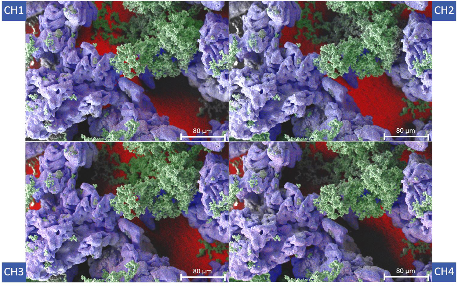
Figure 9: X-ray maps of a rough surface composed of iron and kaolinite on a carbon substrate acquired in an SEM with four SDDs arranged around a center hole for the electron beam (as shown in Figure 3a). On a rough surface each detector has a different view of the specimen, and some X-rays will be blocked from reaching the detector (the shadow effect). When the signals from the four channels are combined, the shadow effect would be largely mitigated (not shown). In these maps the blue, green, and red regions correspond to Fe, Al, and C, respectively. The maps (1024 × 768 pixels) were acquired in 5 minutes at 10 kV and 0.38 nA. Image width (field of view) = 368 μm.
A particularly difficult compositional imaging task is to acquire X-ray maps from microstructures with Li-rich phases. Figure 10a shows an X-ray spectrum of a lithium battery material. The Li-K peak at 54 eV is clearly separated from the noise at the far left, and the oxygen peak is at 525 eV. Figure 10b shows a composite of two X-ray maps revealing the locations of a lithium-rich phase (magenta) and an oxygen-rich phase (green).
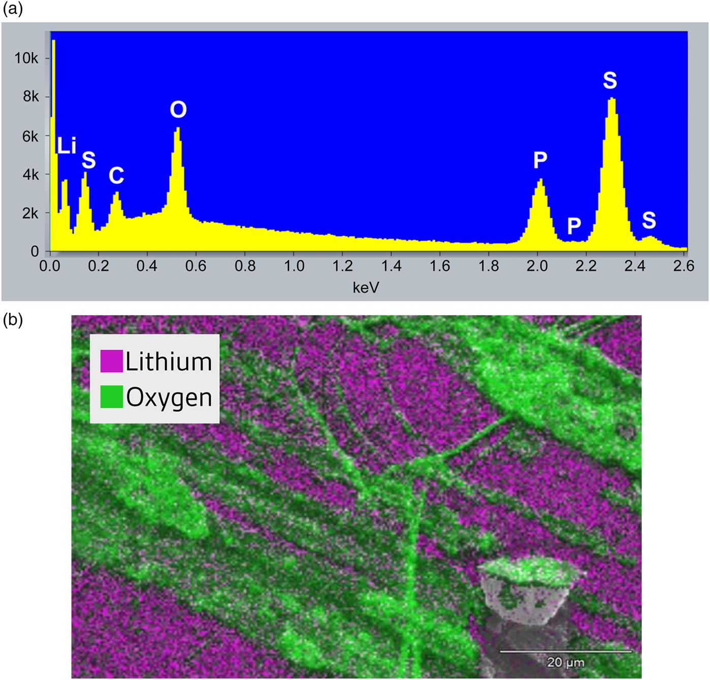
Figure 10: Lithium mapping in battery research. (a) X-ray spectrum acquired at 5 kV showing the Li-K line at 54 eV, the first peak separated from the noise at the left. Carbon and oxygen K lines are at 277 eV and 525 eV, respectively. The spectrum also shows phosphorus and sulfur K and L lines. The total noise of the system was below 2 electrons (rms). (b) Composite of lithium (magenta) and oxygen (green) X-ray maps. Image width = 88 μm. Courtesy of Thermo Fisher Scientific.
Commercial systems
Several companies fabricate SDD chips and modules for use in X-ray microanalysis systems: PNDetector, Amptek, and Ketek [17] are currently the three major players in the field of high-quality SDDs. These original equipment manufacturers (OEMs) supply SDD chips to several producers of complete X-ray spectrometer systems that combine the SDD with user-friendly spectrum-imaging software for microanalysis in the SEM and TEM. Some research laboratories have employed specialized SDDs in large instruments such as particle accelerators and synchrotrons.
Conclusion and Outlook
In the years since the 1984 introduction of sideward depletion by Gatti and Rehak, what is now known as the silicon drift detector (SDD) has had an important influence on the detection of ionizing radiation in a number of scientific instruments. This is particularly true for X-ray spectrometer systems for electron microscopes. These systems are compact, robust, do not require liquid nitrogen, and are capable of high count rates while maintaining exceptional energy resolution. The future of SDD technology is bright: multi-channel pixelized SDDs that increase the count rate capability are currently under development. In addition, new integrated amplifying schemes are being developed to get even closer to the Fano limit at very low X-ray energies.
Acknowledgement
The authors appreciate the constructive comments and discussions with Charles Lyman, Lehigh University.


