


Introduction
Ernst Ruska built the first transmission electron microscope (TEM) during his doctoral studies, and it celebrates its eightieth anniversary this year [Reference Knoll and Ruska1–Reference Freundlich3]. Interestingly, this system was built and was operational less than a decade after experimental results from Davisson and Germer proved de Broglie's hypothesis about the dual wave-particle nature of electrons [Reference Davisson and Germer4,Reference de Broglie5]. Optical microscopes inspired the first TEM, and since then several new imaging modalities have been implemented, such as electron holography [Reference Gabor6,Reference Cowley7], Lorentz electron microscopy [Reference Hale8], and scanning TEM (STEM) [Reference Crewe9]. Even with the introduction of new imaging modalities, the electron microscope developed by Knoll is remarkably like machines in use today. However, in these past eight decades, TEMs have continued to gain capabilities such as energy dispersive X-ray spectroscopy (EDX) [Reference Castaing11], electron energy loss spectroscopy (EELS), annular dark field (ADF) detectors, and aberration-corrected optics both in the TEM and STEM modes.
These advancements have allowed the S/TEM to play a crucial role in analyzing nanometer-scale structural phenomena in physical and life sciences. It has helped tie together the structure-property relationships in materials systems as diverse as interfaces [Reference Stone12], superlattices [Reference Yadav13], domain walls [Reference Nelson14,Reference Mukherjee15], grain boundaries [Reference Gibb16], nanoparticles [Reference Yang17], and catalyst surfaces [Reference Ciston18]. This has led to the discovery of novel applications such as phonon modes at polar vortices and two-dimensional electrical liquids at oxide interfaces [Reference Hoglund19–Reference MacLaren and Ramasse21]. In the physical sciences, these applications have been in fields as diverse as lithium-ion batteries, catalyst systems, and alloy designs to integrate electronic circuits [Reference Zachman22–Reference Korgel26]. Hardware advancements in electron microscopy, such as specialized holders for cryogenic, heating, biasing, or liquid-cell work have also enabled nanoscale studies of dynamic systems such as materials under mechanical strain, thermal gradients, switching behavior in oxide ferroelectrics, and reaction phase systems such as catalysts. So extensive have been the advancements that microscopists have rightly pointed out that the modern TEM with its capabilities for electron imaging, electron diffraction, spectroscopy, and operando studies is “A Synchrotron in a Microscope” [Reference Brown and Rodenburg27,Reference Ramasse28].
Along with the advancements in physical sciences, TEMs have been an absolute game changer for observing biological tissue. Biological TEM followed the development of the original electron microscope closely, with Ernst Ruska's brother Helmut using the TEM for imaging bacteria and viruses as early as 1939 [Reference Ruska29]. The development of cryogenic sample processing and microscopy, combined with ultra-fast high-sensitivity direct electron detectors, have opened the entire world of biological systems such as viruses and individual proteins. As the global coronavirus pandemic continues its onslaught worldwide, some of the most widely circulated electron microscopy images have been cryo-EM images of the SARS-CoV-2 virus.
The Transition to Computer-Enabled Electron Microscopy
However, as Kirkland observed, advances in microscopy and computers happened almost independently of each other for the first few decades of electron microscopy, with computation most used for simulating electron microscopy images [Reference Kirkland30]. This situation persists to a certain extent, and a significant portion of electron microscopy as practiced today is often anecdotal and susceptible to operator bias. Electron transparent samples require significant manual input for their preparation, and the regions of interest (ROI) that are imaged are decided by the microscopist. This region is often chosen based on the visual intuition of a trained microscope operator and the data collected from the ROI only. While automated sample preparation and interfacing with electron microscopes are outside the purview of the current perspective, this current situation is a direct consequence of the fact that microscopy and its associated analysis have continuously operated in a storage and computation-constrained world. Thus, it fell upon a trained microscopist to choose which areas to image and which images to analyze.
Several changes have made microscopy and computation much more closely coupled. First, several individual lens parameters, such as aberration and astigmatism, have been abstracted away due to the computer-controlled operation of individual microscope components. This was necessary due to the advent of aberration-corrected electron optics, which iteratively minimized lens aberrations through a combination of multiple quadrupole, hexapole, and octupole lenses. Second, electron microscopy has almost entirely moved away from using film as the data acquisition media in favor of CCD- and CMOS-based detectors.
As a result, S/TEM alignment, operation, and data collection have become significantly automated. Thus, the volume of data that can be generated in a single day of microscopy is often several terabytes, while current-generation fast direct electron detectors can generate tens of gigabytes of data in a minute. Similarly, in situ experiments with modern detectors, which often have 4k pixels along a dimension, are often run for several hours and generate hundreds of gigabytes of data per hour. Currently, very few microscopy facilities have on-site computational capabilities to compress, process, and archive such data streams from microscopes in real-time, let alone use that data for decision-making to drive automated experiments. Several recent publications, notably a recent perspective by Spurgeon et al. [Reference Spurgeon31], have raised the issue of the volume of data generated by modern electron microscopes and the communities’ scattered responses in dealing with the issue.
Thus, there is a need for integrating on-site microscope facilities with computing and storage systems, at the local or remote edge, to form seamless ecosystems wherein significant measurement collection and instrument steering operations can be automated and remotely orchestrated. In the coming sections, we will give a brief overview of the data deluge in electron microscopy, briefly discuss current computational efforts in the field, and elucidate the path forward for edge computing infrastructure for electron microscopy in the materials community.
Multidimensional Electron Microscopy Enabled by Detector Advances
Electronic detectors have been used for TEM image acquisition since the early nineties. For a long time, such detectors were charge-coupled devices (CCD). However, these detectors were indirect, as the CCDs did not record the electrons themselves. Instead, the electrons would interact with scintillators. The scintillators would convert electrons to photons, which were transferred to the detector through fiber optics that coupled the detectors with the scintillators. However, such a setup degrades the detector quantum efficiency (DQE) and blurs the detector point spread function (PSF) for electron detection. Issues with scintillators are also present for X-ray photon detection and, thus, over the last two decades semiconductor-based direct detectors have been designed, initially for synchrotrons to detect X-ray photons and subsequently for electron detection. Direct electron detectors record individual electron impingement events without intermediate conversion to photons and thus mitigate the DQE and PSF issues with scintillator coupled detectors. A side effect of direct electron detectors is that, along with DQE, the PSF also improves. This impetus for direct electron detectors was from the biological cryo-EM community, where the samples are often highly susceptible to electron dose rates with the maximum allowable dose often below 10e–/Å2.
Along with improvement in detection capabilities, the speed of detection devices has also improved. Again, this was partly driven by cryo-EM as samples degrade rapidly when exposed to electrons. Modern direct electron detectors employed for 4D-STEM experiments can capture over 10,000 frames per second, with the camera developed at the Lawrence Berkeley National Laboratory (LBNL) capable of 87,000 frames per second [Reference Ercius32].
After speed and sensitivity, the third focus area of electron detector research is “dynamic range.” Dynamic range refers to the ratio between the highest and lowest electron flux that can be detected simultaneously. While a detailed discussion about detector geometries is beyond the scope of this perspective, dynamic range issues can often be solved by using hybrid-pixel array detectors [Reference Plotkin-Swing33]. The first such detector used for electron microscopy was the Medipix detector developed at the Diamond Light Source Synchrotron facility in the United Kingdom [Reference van Gastel34]. The second such effort, also a result of synchrotron detector work, is the Electron Microscope Pixel Array Detector (EMPAD) developed at Cornell University [Reference Tate35,Reference Philipp36]. The EMPAD family of detectors is specifically optimized for high dynamic range (HDR), with EMPAD2 reaching a 100,000:1 range for detection. HDR detectors have advantages in both EELS and 4D-STEM experiments since, in both cases, the ratio between scattered and un-scattered electrons may be very high.
4D-STEM datasets obtained from EMPAD detectors broke the TEM resolution limits of 0.4Å in 2018 [Reference Jiang37] and 0.25Å in 2021 [Reference Chen38] by using electron ptychography. Elastically scattered electron diffraction patterns (the 4D-STEM dataset) were used to solve for the microscope lens parameters and the transfer function of the sample being imaged. The second result reached the resolution limit before thermal vibrations from atom columns overtook lens aberrations as the primary source of blurring [Reference Chen38]. Ptychography results have demonstrated that given enough redundancy in 4D-STEM data it is possible to completely deconvolve the electron lens transfer functions, probe decoherence, and positioning errors from the dataset to generate the pure material transfer function. As a result, the final image quality is significantly better than what can be obtained through classical aberration-corrected STEM imaging, with the added advantage of requiring lower electron dose rates [Reference Chen39].
Because of these advantages, many electron microscopes have been retrofitted with faster direct electron detectors for imaging, EELS, and 4D-STEM experiments. These advancements have made the modern STEM truly multidimensional and multimodal, combining imaging, diffraction, and spectroscopy in a single instrument. Some of the most significant advancements in electron microscopy have been possible due to the advent of high-speed direct electron detectors with DQE values approaching unity when combined with single-electron detection sensitivity [Reference Faruqi and McMullan40,Reference Faruqi and McMullan41].
Quantitative Analysis from Electron Microscopy Datasets
Advancements in microscopy hardware have made the extraction of quantitative information from electron micrographs possible. Several recent open-source software packages have been developed to enable this. Some examples include STEMTool [Reference Mukherjee and Unocic42,Reference Mukherjee43], py4DSTEM [Reference Savitzky44], Pycroscopy [Reference Somnath45], PyXem [Reference Cautaerts46], pixSTEM [Reference Nord47,Reference Paterson48], and LiberTEM [Reference Clausen49]. Each package focuses on a specific area of TEM analysis, such as Pycroscopy's focus on image processing or py4DSTEM's focus on 4D-STEM data analysis. The most common area of software development appears to be 4D-STEM, with pixSTEM, LiberTEM, and STEMTool all focusing on it. This focus on 4D-STEM is driven by the fact that such datasets are very complex and thus computational analysis is essential. However, since modern STEM is effectively a multimodal equipment, many other large multi-gigabyte datasets are also routinely generated, such as spectral maps from EELS or EDX and long-duration in situ TEM experiments.
In single-particle cryo-STEM, large datasets of more than several hundred gigabytes are routinely captured before alignment and particle picking. A brief search of the Electron Microscopy Public Image Archive (EMPIAR) [Reference Iudin50] locates hundreds of datasets larger than several terabytes. The cryo-EM community has converged on a few open-source solutions such as Relion [Reference Zivanov51] or commercial software such as cryoSPARC [Reference Punjani52] for particle reconstruction from images, while the materials science community is more diverse in its software choices.
Along with software development, advances in computational capabilities, including accessible CPU/GPUs, implementation of algorithms, and physical models, have led to significant developments in computational simulations spanning a range of time and length scales. Therefore, using either experimental or simulated data to construct artificial intelligence (AI)- and machine learning (ML)-based frameworks for analyzing microscopy datasets is common.
While many studies involve utilization of already developed classification or regression algorithms, frameworks to appropriately find features of interest (such as atoms or defects) from images, capturing dynamic behavior of the systems, and finally porting them to a simulation environment for a comprehensive understanding of the material are still in their infancy. Even though the primary software used for analysis codes, such as PyTorch [Reference Paszke and Wallach53], TensorFlow [Reference Abadi54], Scikit-Learn [Reference Pedregosa55], and JAX [Reference Bradbury56], are all open-access, materials- or problem-specific workflows are often not made public. However, the learning curve required for adapting to existing workflows can be challenging and time-consuming. This is applicable even for simulation packages, most of which are developed in C++, FORTRAN, and Java programming languages, that may not be straightforward. Alternative ways of using these programs rely on open-source post-processing codes. A list of available and widely used tools includes p4vasp, vasptools, OVITO [Reference Stukowski57], Atomsk [Reference Hirel58], Packmol [Reference Martínez59], Avogadro [Reference Hanwell60], ASE [Reference Larsen61], LIGGGHTS, ParaView, PyMol, VMD, and Vesta. The challenge of making these flexible and extensible to process various outputs generated in different formats with varying accuracies, along with integrating them with an experimental setup, remains to be addressed.
Toward Edge Computing in Electron Microscopy
Because of the multiple modalities of data generated with an electron microscope, there is often diversity in terms of size, shape, and generation rates. Thus, there is no single computational solution for analyzing and automating microscopy experiments. Microscope simulations and training can occur on HPC systems, while initial analysis and trained models should be run on connected edge-computational systems, which have low latency between the microscope detectors to the computer memory. HPC refers to systems that are composed of multiple, often thousands of, CPUs and GPUs. These are often monolithic systems with megawatts of power consumption. HPC systems are very rarely used all at once by a single program and are often used by multiple groups running multiple programs simultaneously. Compared to HPC, edge computing is a more recent term and refers to systems intermediate in capability between HPC and desktop systems. HPC systems often have multiple GPUs, with a power draw of several kilowatts. The system currently deployed at ORNL has Nvidia DGX boxes as the edge system, while the HPC system is Summit, which is currently the fourth fastest computer globally with a peak of 200 petaflops. ORNL will transition to Frontier in the coming months, which is the fastest system globally and the only exascale computer currently available.
Ongoing Edge-Computing-Enabled Automated Electron Microscopy Experiments in the Physical Sciences
A typical experimental STEM workflow proceeds as follows. First, a 2-dimensional high-angle annular darkfield (HAADF) image is obtained over a relatively large area. Then, a human operator selects a ROI for more in-depth exploration based on prior knowledge and specific phenomena they are interested in (for example, properties around dopants and defects) or, in some cases, a simple “educated guess.” Here, the “in-depth” exploration refers to acquiring a 1D or 2D spectroscopic signal in designated pixels of the 2D image that measures a function (property) of interest (Figure 1a–1c). Alternatively, one can measure a spectroscopic signal in every pixel of the original image. However, the behaviors of interest are typically localized in relatively small regions of the sample. The entire grid scan is time-consuming, usually imparts a very high electron dose to the specimen, and is only reasonable without prior knowledge about the system.

Figure 1: Deep kernel learning from microscopy data. (a) HAADF-STEM atomic-resolution image used as the starting point for patch identification. Multiple varieties of image patches exist, from pure MoS2, to MoS2 with dopants. (b) Multimodal datasets accompany the atomic resolution HAADF-STEM image, such as simultaneously collected EELS or 4D-STEM datasets. (c) The multimodal datasets are scalarized to develop relationships with the imaging data. This scalarization can be of the peak maxima for EELS spectra or center of mass for 4D-STEM diffractograms. (d) An active learning module can be built to reside on a connected edge computing system that takes in the features from the HAADF-STEM images and relates them to the scalar features in the correlated multimodal datasets (EELS or 4D-STEM). Adapted with changes from [Reference Roccapriore67].
Such a setup can be used for automated analysis of multidimensional datasets. Ophus et al. have demonstrated that the py4DSTEM package can be integrated with microscope data acquisition for automated crystallographic orientation mapping [Reference Ophus62]. In another example, it was demonstrated that the obtained 4D-STEM datasets can be used to perform single sideband (SSB) ptychography [Reference Pennycook63] in real time by using GPU-based solvers on a connected edge system [Reference Pelz64,Reference Pelz65].
Recently at ORNL, a probabilistic machine learning workflow for intelligent sampling of measurement points toward physics discovery was demonstrated. The approach is based on deep kernel active learning (DKAL) that combines a deep neural network with a Gaussian process and allows learning relationships between local structure and functionality encoded in spectra on-the-fly. Each measurement informs the subsequent measurement by increasing the model's knowledge base for the structure-property relationship of interest. It was first demonstrated for the bulk and edge plasmon discovery in STEM-EELS experiments and later applied to rapid studies of symmetry-breaking distortions and internal electric and magnetic fields in 4D STEM experiments on graphene (Figure 1) and MnPS3.
A DKAL experiment starts with featurizing a 2D HAADF image by splitting it into patches at each pixel coordinate. The patch size can be determined by the characteristic length scale of the structure of interest, or it can be chosen ad hoc (Figure 1a). The next step is to determine a scalarizer function, that is, a function that converts a spectral signal (Figure 1b) to the physical structure of interest. The scalarizer can, for example, be a peak energy or maximum intensity of selected mode(s) in EELS, or the center of the mass shift in 4D-STEM (Figure 1c). It can also be based on more advanced analyses, such as those involving physics-based inversion of the 4D-STEM data toward the scattering potential with a subsequent selection of the associated features of interest. After featurizing the structural image and defining the scalarizer, several measurements in randomly selected pixel coordinates are obtained and corresponding image patches and scalarized spectra used to train a DKL model. The trained model is then used to predict the next measurement point. After performing a measurement at the suggested location, the training set is updated and the model training and prediction steps repeated. The process is iterated until the experimental budget is exhausted, the uncertainty in predictions falls to a required level, or the required predictability is achieved (Figure 1d).
Based on this scheme, automated experiments in both STEM-EELS and 4D-STEM using DKL were performed in real time [Reference Roccapriore66,Reference Roccapriore67]. NION microscopes were used where the NION Swift control software allows flexible Python-based control of the microscope hardware elements needed to conduct automated experiments [Reference Meyer68,Reference Meyer69]. An example [Reference Roccapriore66] highlights the use of automated experiments where a previously unknown plasmon edge mode in 2D MnPS3 was discovered using the DKL approach. By scalarizing the EEL signal in such a way as to maximize a ratio of low-energy to high-energy spectral peaks, the correlation between material edges and this EEL peak ratio was actively learned during the experiment. For beam-sensitive specimens like MnPS3, automated experiments are even further justified. In the context of 4D-STEM, diffraction patterns can be scalarized according to center of mass shifting and correlated to structural features in graphene where the exploration of the sample can be performed by learning where the maximum center of mass shifts are most likely to occur.
From the Edge Computer to High-Performance Compute Clusters
Comprehensive studies utilizing an open-access, overall framework capable of directly mapping between experimental observations and computational studies using deep learning approaches are still in their developmental stages. The primary roadblocks are the difference in time, length scales between two regimes, and associated latencies to model and understand a physical behavior. At ORNL, a deep learning-based framework to address such challenges has been developed by employing deep convolutional neural networks to identify atomic features (type and position) in a material. Specifically, features within the AtomAI utility functions were used to construct a bulk conventional unit cell, supercell, or surface, based on the type of simulations performed and material properties of interest [Reference Ziatdinov70,Reference Ghosh71]. Post-AtomAI analysis, initialization of numerical simulations to find the optimized geometry and temperature-dependent dynamics of system evolutions are used. The outputs, along with associated uncertainties in predictions at various levels, are obtained using this framework. These may subsequently be used to evaluate and modify experimental conditions and ROIs to drive an automated experiment and to build a platform that can “learn” material properties on-the-fly during an experiment. This entire framework can be performed such that observational data are directly transferred from a microscope to an edge computer, such as the Jetson AGX Xavier. This GPU-based platform is then used to analyze, train, or tune pre-trained DL models, followed by simulations using CPU-based HPC resources. Altogether, the feedback from measurements, simulations, and DL models are then introduced back to the workflow to guide experiments while learning from theoretical models [Reference Ghosh72].
Seamless Connectivity Between Microscopes, Edge Systems, and HPC Clusters
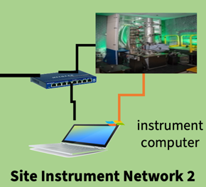
The schematic of the system at ORNL is demonstrated in Figure 2. The scheme connects two separate electron microscopes. Each microscope has a connection between the microscope and the control computer, while the control computer is connected to a gateway workstation and network-assisted storage (NAS) through a site gateway switch. Through this gateway switch, the gateway workstation can be connected to lab-area HPC resources and remote HPC resources (such as NERSC at the LBNL) through wide-area networks. Recently, our team successfully used this setup to deploy a prototype system at ORNL; its connectivity diagram is demonstrated in Figure 3 [Reference Mukherjee73,Reference Al-Najjar74]. The workflow is executed as follows: the operator starts a Jupyter session on the data center and enters the desired microscope operation, with the notebook session itself operable from any system on the network with verified credentials, as visualized through Process 1. This operation script is transmitted through the Pyro client to a server running on NION Swift on the microscope control computer, as shown by Process 2. NION Swift running on the control computer executes this script through Processes 3 and 4. The output data from the microscope detectors are streamed to the NAS (Process 5), with the state of the data collection communicated to NION Swift (Process 6). Since the NAS is also samba-mounted on the cluster, these data are available immediately, as shown through Process 7. As the data are collected on the NAS, the cluster starts processing it with the results being available to the operator as outputs in the Jupyter session.

Figure 2: Schematic of connection between the microscope and high-performance computing through network-assisted storage gateways. The schematic shown here demonstrates a setup for connecting two separate electron microscopes to a common internal network gateway, along with access to remote HPC systems through wide-area connections.

Figure 3: Current setup at ORNL for remote access and on-demand microscopy data transfer between remote workstations and NION microscopes. The communication between the microscopes, control computers, and network-assisted storage has eight separate components. The components themselves can be classified into data transfer (blue), management (green), and control (red) processes.
Data Management Through Compression and Open-Source File Formats
A challenge in coupling microscopes and compute clusters is that they are often geographically separated; thus, the bottleneck is often network connections that slow data transfer. Many of these issues can be mitigated by developing physics-informed compression techniques, with the compression routines residing on the edge computer and transferring only compressed data to HPC clusters on the network. Both lossless and lossy compression are avenues that should be explored. Many current techniques, such as 4D-STEM strain mapping or EELS mapping, which focus on small data sections, would benefit tremendously from lossy data compression techniques.
Additionally, large datasets are often composed of multiple individual frames, which can be CBED patterns in 4D-STEM, or individual frames in cryo-STEM or in situ TEM. In each of these cases, individual frames are often really similar to neighboring frames in a single dataset and are thus low-entropy datasets. Arithmetic coding-based lossless compression approaches can be potent in many instances, leading to data compression by several factors. Compressed data should be stored in open-source data formats, and codes on HPCs should be built to work directly on compressed data without decompressing the data on the cluster.
In the last several years, a few groups in the materials community have tackled the issue of data storage formats. This has led to development of open-source microscope data containers capable of performing provenance tracking, such that compressed data and analysis can live together in a single dataset. Work in this area has led to the development of the EMD data format [Reference Ophus75], which is based on the open-source HDF5 specification. Other recent work at ORNL has been the Universal Spectroscopic and Imaging Data (USID) [Reference Somnath76,Reference Somnath77], which has been accompanied by the open-source pyUSID package to read and write USID datasets [Reference Somnath78].
Future microscopy systems should directly stream data from detectors to GPUs on a connected edge system, where online compression can be performed on the data being streamed. Alongside this, compressed data should be streamed to HPC systems, where the data are processed and stored in open-source data containers, and the processed results, which are often significantly sparser, streamed back to the microscope operator. The processed data can also be fed into decision-making algorithms, which can be used to drive the microscope for results-guided automated experimentation. This setup will, however, lead to networking challenges, as data, decisions, and output will be streamed simultaneously. This will require the development of reliable switching and networking protocols to couple the microscopy and computation.
Continuous Provenance Tracking Through Digital Twins on Connected Edge and HPC Systems
As mentioned previously, a goal for the development of data containers is storage of metadata in machine-readable formats and provenance tracking. While microscope data files are often multidimensional arrays, making sense of them requires access to metadata. Based on the authors’ experience, current vendor-generated metadata is frequently incorrect and needs significant manual intervention to correct the data. Secondly, over the course of an experimental session, microscope parameters often “drift” and the stored metadata may reflect the initial starting conditions, while later experiments may be significantly different.
Modern microscopes have sensors that generate information about individual lens and holder parameters, often in real time. One way to use these data is to build virtual infrastructure twins, where a simulation of the microscope runs on a cluster, which is updated in real time based on individual lens values. Such a system can then save the digital twin of a microscope and provide detailed provenance tracking at every time point of an experiment with errors in metadata noted if the observed sensor outputs don't match. Notably, a setup like this would eliminate the need for a skilled operator to verify the accuracy of the metadata and generate the state of the microscope while analyzing the data, allowing for significantly more complex autonomous experiments where the microscope's parameters change during an experiment.
Additionally, continuous state monitoring opens the door for Bayesian predictive experiments. Whether it is for inverse problems such as ptychography, or for in situ experiments, provenance tracking provides completely automated, predictive science. These data are already available, but are rarely collected in a single location in a machine parsable format. In situ holders for heating, biasing, or chemical reactions track the states continuously, while most modern microscopes track individual lens currents and settings. However, as far as the authors know, these datasets have not been used to build a digital microscope twin yet. Building a highly accurate digital twin also removes the need for conducting multiple experiments. Future systems will thus be able to run completely virtual experiments and collect experimental data from a real-world microscope only when needed.
Conclusions
The challenges and opportunities we demonstrated in the roadmap above demonstrate that this is an exciting time for electron microscopy. Two fields, data science and microscopy, are coming together. Future microscopes will not be standalone systems, but multi-purpose scientific tools tightly coupled to local edge and remote HPC computational facilities. The current divisions in physical sciences between materials synthesis, characterization, and theory are not the future. All three aspects can and should be present in a single setup that can autonomously “learn the physics” directly from the experiment. Literally, a “Lab on a Beam” [Reference Kalinin79].
Acknowledgements
This research was sponsored by the INTERSECT Initiative as part of the Laboratory Directed Research and Development Program of Oak Ridge National Laboratory, managed by UT-Battelle, LLC, for the US Department of Energy under contract DE-AC05-00OR22725. This research used resources of the Center for Nanophase Materials Sciences, which is a DOE Office of Science User Facility.
This manuscript was authored by UT-Battelle, LLC under Contract No. DE-AC05-00OR22725 with the U.S. Department of Energy. By accepting the article for publication, the publisher acknowledges that the United States Government retains a non-exclusive, paid, irrevocable, world-wide license to publish or reproduce the published form of this manuscript, or allow others to do so, for United States Government purposes. The Department of Energy will provide public access to results of federally sponsored research in accordance with the DOE Public Access Plan (http://energy.gov/downloads/doe-public-access-plan).


