


Introduction
“. . .we introduce a new type of microscope capable of investigating surfaces of insulators at an atomic scale . . .”
The words above are taken from the paper by Binnig, Rohrer, and Quate published back in 1986 entitled simply “Atomic Force Microscope” [Reference Binnig1]. As well as having been an ingenious invention in itself, the atomic force microscope (AFM) was seen by the prescient authors as full of potential. Some of that promise took quite a few years to come to fruition, but the predictions of the authors have been borne out.
The AFM is probably the most well-known member of the family of techniques called scanning probe microscopy (SPM). As the name suggests, an SPM involves scanning a probe (or tip) near a surface to build up a three-dimensional image. This is done by measuring some distance-dependent property, typically a current or a force. Depending on the instrument design, the sample can also be scanned under a fixed probe. The AFM evolved from the scanning tunneling microscope (STM), which in turn builds upon Young’s topografiner. In 1972, Young built an apparatus that measured topography by generating a field emission current between the probe and sample [Reference Young2]. It then scanned the emitter over the sample and used feedback in the vertical (z) axis of the scanner to maintain the emission current.
The STM is similar to the topografiner but uses the quantum tunneling effect, which is much shorter-ranged and produces significantly improved resolution. Early on in its development the STM achieved atomic resolution [Reference Binnig3], which is now quite routine. A significant limitation with STM as a microscope, however, is that the whole sample has to be conductive. If the tip passes over even a small non-conductive material, the scanner will drive the tip into it, which will likely damage both the tip and sample. The AFM emerged as a solution to this and for measuring non-conductive samples more generally. While the AFM can also achieve atomic resolution in some circumstances, the strength of this technique lies in its wider applicability, both in air and in liquid. This is particularly important for analysis of biological specimens. This article reviews the development of AFM methods in light of statements made in the original Binnig, Rohrer, and Quate paper [Reference Binnig1].
Operating Principles
The next few paragraphs show how various methods of AFM fabrication and operation were predicted in the Binnig et al. paper.
Microfabrication of the cantilever
“. . . eventually microfabrication will be employed to fabricate a spring” [Reference Binnig1]. At the center of an AFM is a micro-fabricated cantilever—much like a diving board—which usually has a sharp tip at the end pointing down toward the specimen. When the tip interacts with the specimen it causes a deflection in the cantilever. In most modern AFMs force sensing is accomplished by a technique called optical lever detection. The cantilever motion is amplified by aiming a laser beam at a mirror surface on the back of the cantilever. A detector some distance away collects a magnified signal of cantilever motions (Figure 1). As the cantilever is scanned over the surface laterally, the cantilever deflection will go up and down as it follows the topography of the specimen.

Figure 1 Schematic diagram showing the sample, tip, cantilever, and laser deflection measurement system used in most modern AFMs.
Contact mode
“A feedback loop is used to keep the force acting on the stylus at a constant level” [Reference Binnig1]. As the force experienced and exerted by the cantilever is dependent on the bending of the cantilever, it is necessary to maintain a fixed level of force. This is done with a feedback controller that works in much the same way as the electronics that keep a temperature controlled stage at a set value, so that whenever the force is too high, the z scanner pulls the tip up and vice versa. This was the first mode of operation, usually referred to as contact mode, which looks only at the bending of the cantilever. Its biggest disadvantage is that the lateral forces can be rather high and can be damaging to delicate samples.
Intermittent contact mode
“In the second and third modes, the lever carrying the diamond stylus is driven at its resonant frequency in the z direction” [Reference Binnig1]. An alternative, already identified by Binnig et al. in their original paper, is to drive the cantilever to resonate. In this mode the tip taps the surface and tends to be more forgiving of delicate samples. This mode has a number of different names depending on the manufacturer of the instrument used. A good general term is intermittent contact mode, where the feedback is on the amplitude of the oscillation. Figure 2 shows an image from this mode of human dental enamel after exposure to acid.

Figure 2 Intermittent contact mode image of human dental enamel after exposure to 10 mM HCl. As is usual with AFM images, a color scale is used to indicate the height of the sample. In this case the z range is 250 nm from black to white. Scan size = 50 μm × 50 μm. The image shows clearly oriented ridges in the enamel. Sample courtesy of Dr. Christine Mueller-Renno, TU Kaiserslautern, Germany; and Prof. Dr. Matthias Hannig, Uniklinikum des Saarlandes, Germany.
Phase signal
“Either [amplitude or phase] can be used as a signal to drive the feedback circuits” [Reference Binnig1]. The original paper also predicted that the phase signal—the time delay between driving the tip to resonate and the measured response—could be important. It has turned out to be very useful over the years to map material properties in a qualitative manner and to resolve molecular conformations in polymers, such as the stem-to-stem overhang of polyethylene molecules at the crystal-amorphous interface [Reference Savage4]. Recently, frequency modulation, which makes use of the phase signal, has proven beneficial on specimens containing fine surface features, particularly in vacuum systems, to achieve resolution comparable to the best STM images [Reference Giessibl5]. A similar but a priori simpler technique, phase modulation AFM, is well suited for the acquisition of images at atomic and molecular resolutions in liquid environments [Reference Ackermann6].
Beyond Topography 1: Force Measurements and Mapping
Early AFM images showed mainly the topography of the surface in the manner of a highly sensitive profilometer. However, what sets AFM apart from most other microscopy methods is its ability to measure material properties on a scale of nanometers. Again, Binnig et al. foresaw this possibility.
Force measurements
“Therefore, we should be able to measure all the important forces that exist between the sample and adatoms on the stylus” [Reference Binnig1]. Force spectroscopy is a key part of AFM use. It involves making use of the force-sensing capabilities of the AFM to measure adhesion, or to indent surfaces to extract, for instance, stiffness parameters. The methodology is to move the cantilever vertically toward the surface and then to retract the cantilever again once a chosen force is reached. Careful monitoring of the deflection of the cantilever is important, so a sensitive detection system is a significant advantage. The resulting data are usually two curves (one for approach and one for retraction), with distance on the x-axis and force on the y-axis. On the approach to the surface the tip may indent the specimen and simultaneously deflect. Simply by subtracting the deflection of the cantilever from the movement of the vertical scanner it is possible to measure the amount of indentation. Fitting known elasticity models (such as the widely used Hertz model) to the resultant force-distance curve enables a measurement of the Young’s modulus of the specimen. Furthermore, when retracting the tip from the surface it is possible to measure non-specific adhesion events. This can be a means of distinguishing hydrophobic and hydrophilic regions because in standard laboratory humidity conditions, hydrophilic regions will show higher adhesion forces.
Protein unfolding
Another area in which a retracting AFM tip can be of interest is that of elucidating protein structures. When one end of a folded protein is tethered to the substrate and the other tethered to the tip when the cantilever is subsequently pulled away, the protein will begin to unfold. The typical curve will have a saw-tooth appearance, which comes about by the sequential unfolding of each domain. For each tooth of the saw, the tension gradually increases until a domain unfolds whereupon it suddenly decreases and starts to increase again as the molecule becomes taut again and begins to pull at the next domain. This kind of force spectroscopy has been very useful in measuring protein kinetics, but it has a drawback because the vertical scanner is being moved at a constant rate, while the tension keeps changing as described above. Thus the actual loading rate is hard to assess. This is where another technique called force clamping has a distinct advantage. Instead of pulling the vertical scanner at a constant rate, the tension on the cantilever is maintained as far as possible, so that the z-scanner only moves when a domain unfolds. Thus the unfolding process becomes a statistical process looking at how long a domain can typically remain folded at a given tension. These single molecule measurements push the sensitivity limit of AFM, and so the complementary technique of force-sensing optical tweezers is also a good choice. Optical tweezers can maneuver beads with molecules attached in order to stretch them. In the case of JPK’s NanoTracker™ 2, the force is measured much in the same way as in an AFM: the trapping laser is monitored by a quadrant photodiode.
Force mapping
Whether the interest is in stiffness or adhesion measurements, an important extension to force spectroscopy is force mapping [Reference Radmacher7], which is simply performing force spectroscopy on a grid of points. Historically this was a very slow way of obtaining stiffness maps, even low-resolution maps (for example, 64 × 64) would take hours. Software and hardware improvements have led to a new quantitative imaging (QI™) mode, which is able to get high-resolution force maps (for example, 512 × 512) in a matter of minutes (see Figure 3). As an imaging mode it also has a significant advantage in that it is even more forgiving of fragile or loosely attached samples than intermittent contact mode. Another major advantage is that every curve can be saved, so that they can be batch processed in the analysis software, for example to fit an indentation model for a Young’s modulus map. In addition, a contact point analysis may be generated to produce a three-dimensional image of what the surface looked like before being indented. Also tomographic images may be produced at any chosen level of indentation force.

Figure 3 An example of a force-distance curve showing the approach from the right hand side of the plot to a cell surface in light red. The line starts off flat until there is contact with the cell, the force then increases until the chosen setpoint when the tip starts to retract, and the darker red curve is obtained. The curve has been annotated to indicate some of the parameters that can be extracted through software analysis (with the work of adhesion being the area indicated in gray). The four images are of a living fibroblast cell imaged in QI™ mode: (1) Optical phase contrast image with inset region marked for the 25 μm × 25 μm AFM scan; (2) height image at 1 nN (z range = 500 nm); (3) contact point height at zero force (z range = 1 μm); (4) calculated Young’s modulus images (z range = 150 kPa). Fibroblast cells courtesy of R. Schwarzer and Prof. A. Herrmann, Humboldt University, Berlin.
Micro-rheology
For soft materials, micro-rheology can also be a useful AFM operating mode. This measurement involves oscillating the z-scanner at rather low frequencies while the tip is in contact with the sample. The visco-elastic nature of the sample will cause the tip to respond with a delay and a reduction in amplitude. Comparing the z scanner drive and the response can lead to the determination of traditional rheological parameters: the storage and loss modulus of the sample.
Beyond Topography 2: Electromagnetic Properties
From the earliest days of AFM, researchers sought to use the probe to reveal fine-scale magnetic and electrical properties—another prediction from Binnig et al. in 1986.
Magnetic force microscopy
“We envision a general-purpose device that will measure any type of force; not only interatomic forces, but electromagnetic forces as well” [Reference Binnig1]. Binnig and his colleagues predicted that the AFM could be used for measuring other forces beyond interatomic ones. One of the first such techniques, published only a year after the invention of the AFM, was magnetic force microscopy (MFM) [Reference Martin and Wickramsinghe8]. This method usually works as a dual-pass technique wherein a line of topography is acquired in intermittent contact mode, after which the tip is lifted up and hovers at a distance of typically a few tens of nanometers where the magnetic field from the sample can influence the oscillation of the magnetically coated probe. The tip then moves to the next line and gradually, alongside the topographic image, an image of the change in hover amplitude or phase reveals contrast in the magnetic domains on the sample (Figure 4).

Figure 4 Magnetic force microscopy (MFM). Local magnetic force gradient distribution measurements between the magnetic cantilever tip and sample. Overlay of magnetic force information and 3D height image on NiFe square structure, which is 60 nm tall. The magnetic domains and Landau pattern are clearly visible in the colored phase data (a 2-color scale was chosen to highlight the contrast within the NiFe square). Scan size = 8µm × 8µm. Acquired in Hover Mode (dual pass). Sample courtesy of Dr. Katrin Schultheiss, Institute of Ion beam Physics and Materials Research, Helmholtz-Zentrum Dresden-Rossendorf, Germany.
Electrostatic force microscopy
A closely related technique is electrostatic force microscopy (EFM), which can be operated in exactly the same way as MFM, but with an electrically conductive tip so that the change in amplitude or phase on the hover pass represents the strength of the electrostatic force. Another way of obtaining EFM images is with a variation of fast-force mapping (using quantitative imaging, QI™), applying an electrical excitation at the fundamental cantilever resonance. This does not directly cause the cantilever to resonate, but resonance will occur in the presence of an electrostatic force (see Figure 5).

Figure 5 Electrostatic force microscopy (EFM). Electrical force gradient measurements can be made between the tip and sample measured in fast-force mapping mode when there is an electrical excitation at the fundamental cantilever resonance. The data set then contained vertical deflection and amplitude and phase signal of the mechanical response from the electrical excitation. The EFM image here is the amplitude of the cantilever shortly before the point of contact. The sample is an Intel Core i5 processor, where the structures are about 5 nm tall, overlaid with the electrostatic force signal (color scale black-cyan-magenta-white, with black representing the lowest electrostatic force and white the highest). Scan size = 1.4 μm × 1.4 μm.
Kelvin force microscopy
These techniques offer only qualitative electromagnetic images alongside the topographic data obtained by AFM. A modification of the EFM technique allows the surface potential to be measured quantitatively. Kelvin probe microscopy (KPM) [Reference Nonnenmacher9] involves applying an electrical excitation to the cantilever, which causes the cantilever to oscillate if there is a potential difference between the tip and sample. Feedback electronics are used to adjust the potential at the tip so that the movement stops; the point at which the potential at the tip matches the surface potential can be presented as an image.
Conductivity
“The STM could be used as a force microscope by simply mounting the STM tip on a cantilever beam” [Reference Binnig1]. Or, to put it another way, adding tip current measuring electronics to an AFM enables measurement of the conductivity of the sample, while not relying on the sample being conductive everywhere as STM does. Most conductive AFM (CAFM) measurements to date have been in contact mode [Reference Park10], which, in addition to the familiar disadvantages of contact mode, can also lead to the conductive coating on the tip being damaged rather quickly. An elegant solution to this is to use force mapping, such as the fast QI™. It is then straightforward to obtain a map of the peak current with much improved durability of the conductive tip (see Figure 6).

Figure 6 Conductive AFM. A fast-force mapping measurement of a graphene flake on a conductive Ir/Au substrate. The peak current is recorded at each pixel, and the resulting current image is a conductivity map. Top: typical force curve showing the approach curve in red and the current measured through the tip in blue. Bottom: representation of 3D topography overlaid with a color scale of the current image (the brighter the color the higher the conductivity at that location). The graphene flake (black) is less conductive out of plane than the substrate. Scan range = 1.5 µm × 1.5 µm.
Modern AFM Instruments
Binnig et al. did not speculate about what commercial instruments would look like, but it is apt to take a look at the present day state of the art. Important areas of development have been integration with other techniques, faster scanning, and software improvements.
AFM and light microscopy
In terms of integration of the AFM with other techniques, a major feature is the mechanical interface with the inverted light microscope (Figure 7). This enables a wide range of techniques to be combined with AFM, from normal brightfield, phase contrast, or differential interference contrast (DIC) microscopy to increasingly complex techniques such as Raman spectroscopy, fluorescence resonance energy transfer (FRET), fluorescence lifetime imaging (FLIM), fluorescence correlation spectroscopy (FCS), fluorescence recovery after photobleaching (FRAP), confocal microscopy, and super-resolution techniques including stimulated emission depletion (STED) [Reference Harke11] and photo-activated localization microscopy (PALM) / stochastic optical reconstruction microscopy (STORM). An important aspect of this integration is software that enables the combination of data from the AFM and the complementary technique. Mounting the AFM on a high-resolution light microscope also opens up the possibility of using the AFM tip as a means of applying forces locally in order to observe the effects in the light microscope. Examples include calcium imaging on cells that have been poked by an AFM tip and 40 nm fluorescent bead manipulation while observing in real-time with STED [Reference Chacko12]. Recent unpublished data demonstrated simultaneous AFM manipulation of fixed HeLa cells with labeled microtubules and actin-labeled living fibroblast cells in growth media observed by STED microscopy (see Figure 8).
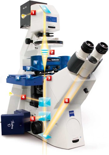
Figure 7 Example of a modern AFM mounted on an inverted microscope. The AFM parts are labeled in blue: (1) NanoWizard 4a AFM head, (2) cantilever holder, (3) petri dish holder, (4) motorized sample stage. The light microscope parts are labeled in red: (1) transmission light source, (2) condenser lens, (3) objective lens, (4) fluorescence excitation path from backport, (5) side port with fluorescence camera, (6) eye piece beam path.

Figure 8 Living human skin fibroblasts in growth medium. Left: silicon red actin staining for STED at 775 nm reveals the cytoskeleton in detail. Scale bar = 1 μm. Middle: AFM Young’s modulus image (color scale black-blue-white is 0–50 kPa) acquired in ROI of STED. The AFM images taken in QI show outer membrane ruffles of <3 kPa. Right: software overlay of STED and AFM images.
Acquisition speed
AFM is often seen as a slow and difficult technique by those who had some contact with it in the early years after its inception. The time to acquire an AFM image was traditionally around 5 to 10 minutes, which meant productivity wasn’t very high. Modern AFM instruments—including the NanoWizard® 4a (Figure 8)—address this limitation by offering some degree of automation and unattended use, through an experiment planner interface and also through control of the software over the internet. Slow scanning can present other difficulties; if the object of interest is either somewhat mobile or likely to undergo a phase change, then a slow acquisition speed can be disadvantageous. Some manufacturers have introduced fast scanning options for their AFM systems that enable images to be obtained in a matter of seconds. This offers a significant benefit for following processes as diverse as exocytotic vesicle budding events on living cells, fibrillogenisis of collagen [Reference Stamov13], and crystallisation from the melt of some thermoplastics (Figure 9).

Figure 9 Four intermittent contact mode phase images of poly(hydroxybutyrate-co-hydroxyvalerate) as it crystalizes from the melt showing one of the advantages of fast scanning. Images are the first, second, ninth, and last images out of a series of 16; each image took about 13 seconds to acquire, with the whole set taking about 3 minutes in total. With traditional scan speeds each image would have taken about 5 minutes, and the detail of the process would be lost. Scan width =1 μm×1 μm.
Software
The view that AFM can be a tricky technique to use has been addressed with numerous improvements, largely in the software. The QI™ mode, for instance, comes with a friendly interface where the user simply estimates the sample roughness and the relative adhesion strength in the given environment with the given tip, and he or she can start imaging from there, usually without needing to make further adjustments. Thus, even inexperienced operators are able to acquire high-resolution AFM images, such as of the intra-molecular structures of the bacteriorhodopsin or DNA molecules [Reference Stamov14].
Conclusions
AFM technology has improved remarkably over the last three decades, and much of this evolution was foreseen by the authors of the original AFM paper: they predicted micro-fabricated cantilevers, force spectroscopy, electrostatic and magnetic force microscopy, as well as conductive AFM. In their 1986 paper they did not describe, however, how much faster and easier to use the technology would become.


