


Introduction
Methods for nanomechanical testing have become a critical part of materials research, with the ever-increasing importance of nanomaterials and nanoscale phenomena in modern technological applications.Reference Dehm, Jaya, Raghavan and Kirchlechner1–Reference Zhu and Chang3 Small-scale mechanical testing can also enable a “minimally invasive” approach to collecting mechanical data from bulk materials, providing information from individual microstructural components to areas of damage accumulation in materials under harsh environments.Reference Kiener, Minor, Anderoglu, Wang, Maloy and Hosemann4 By simultaneously observing deformation phenomena and measuring mechanical response in situ, it is possible to connect nanomechanical testing information to models that describe both the subtlety and complexity of how materials respond to stress and strain. Furthermore, the in situ approach is crucial to obtain insight into the quality of a mechanical test, as small inaccuracies can lead to completely false conclusions. Therefore, quantitative mechanical testing conducted while observing deformation in situ is uniquely suited for studying mechanical properties since the fundamental deformation mechanisms are readily observed.
Starting in the late 1950s, in situ straining stages for electron microscopes were developed that provided dynamic observations of dislocation motion in metals.Reference Wilsdorf5–Reference Berghezan and Fourdeux7 Electron microscopy is well suited for studying the mechanical properties of materials, since high spatial resolution is required for imaging individual defects in heterogeneous materials. However, complex defect structures lead to complications in connecting high-resolution observations to deformation phenomena that are inherently multiscale in nature. Therefore, multiscale analysis of materials is required to fully understand how a material responds to stress. Nonetheless, in situ nanomechanical testing provides the opportunity to apply controlled loading geometries, environments, and sensitive measurements that provide clarity in dynamic microstructural changes.
The study of deformation phenomena has a history going back to the start of high-voltage electron microscopy.Reference Komatsu, Mori and Iwasaki8–Reference Messerschmidt, Baither, Bartsch and Baufeld10 More recently, the introduction of quantitative measurement devices has enabled precise knowledge of the stress inside a sample.Reference Minor, Syed Asif, Shan, Stach, Cyrankowski, Wyrobek and Warren11,Reference Warren, Shan, Syed Asif, Stach, Morris and Minor12 Recent reviews have described the impact of combined quantitative measurement and imaging at the individual defect level.Reference Legros13,Reference Yu, Legros and Minor14 In situ transmission electron microscopy (TEM) nanomechanical testing makes use of the sensitivity of TEM to lattice distortion that allows for visualization of both elastic and plastic deformation via strain fields from a length scale of several hundred nanometers down to the atomic-length scale. Novel correlated imaging and diffraction scanning transmission electron microscopy (STEM) techniques have emerged due to the development of fast detection systems of several hundred frames per second. In situ scanning electron microscopy (SEM) testing allows for observation of the overall morphology of the deformation. With the recent progress in electron channeling contrast imaging (ECCI), transmission SEM, and electron backscatter diffraction (EBSD), SEM techniques have advanced into length scales that were historically covered only by conventional TEM. In situ x-ray diffraction (XRD) testing can identify defect structures and phases at a larger scale than that of TEM and provide access to subtle changes in misorientation. In synchrotrons, focused x-ray beams can probe strains and orientation changes with beam diameters down to ∼10 nm.
Direct observations of defect structures
Physical metallurgy has certainly benefited from direct observations of defect structures, as Kacher et al.Reference Kacher, Kirchlechner, Michler, Polatidis, Schwaiger, Van Swygenhoven, Taheri and Legros15 show in their article in this issue. They discuss mostly TEM-based observations that led to insights into defect–defect interactions and their impact on mechanical properties. Grain boundaries are one of the most common defects in structural materials, but many details of the complex strain accommodation mechanisms at grain boundaries are still unsolved. In situ experiments have been reported that deal with inherent mechanisms in metals that relax stress at grain boundaries, such as grain-boundary migration and grain rotation. In this respect, automated crystal orientation mapping (ACOM) performed by electron diffraction inside the TEM gives information on the evolution of grain size and grain orientation under load and guides the analysis of different grain-boundary mechanisms. While this is especially important for fine-grained and nanocrystalline materials, dislocation–grain-boundary interactions are another topic highlighted in their overview. In service, engineering materials are exposed to complex stress states and high strain rates. The recent advances of in situ nanomechanical testing covering both of these topics is another central point of their overview.
In situ imaging is most useful in the context of connecting defects and structural features with deformation studies. Due to the multiscale and complex nature of defect structures in deformed materials, correlative microscopy techniques in scanning electron microscopy can provide unique insights. In their article in this issue, Gianola et al.Reference Gianola, Britton and Zaefferer16 discuss some of the emerging SEM-based methods for identifying defects, including EBSD, ECCI, and diffraction-contrast STEM. EBSD continues to evolve with faster detectors that enable in situ mechanical testing combined with ECCI and diffraction-contrast STEM, and higher resolution imaging that allow for defect characterization.
Atomic-scale resolved imaging
In their article, Spiecker et al.Reference Spiecker, Oh, Shan, Ikuhara and Mao17 carry the discussion to the atomic scale by employing atomic resolved in situ TEM/STEM experiments to study dislocation generation, multiplication, and interaction with hydrogen as well as dislocation–grain-boundary interactions. The strength of these methods is the direct visualization of defects during deformation. An example provided in their article is screw dislocations intersecting a low-angle tilt grain-boundary-inducing kink formation in the transmitted dislocations and jogs in the grain-boundary dislocation array. Such studies are crucial to understand dislocation–grain-boundary transmission stresses and possible resulting strain-rate dependence. Interestingly, functional two-dimensional (2D) materials such as bilayer graphene can also form dislocations as inherent growth defects, which may alter charge transport in devices. Spiecker et al.Reference Spiecker, Oh, Shan, Ikuhara and Mao17 show that in situ nanomechanics allows for manipulation of individual dislocations, which in turn leads to mechanical switching of stacking sequences of the 2D material,Reference Butz, Dolle, Niekiel, Weber, Waldmann, Weber, Meyer and Spiecker18 a previously unobserved effect.
Local strain measurements
Emerging techniques of measuring local strain around individual defects or groups of defects are discussed by Gammer et al. in their article in this issue.Reference Gammer, Richard and Eberl19 Digital image correlation is one of the most readily available methods for strain measurements using light optical or electron microscopy imaging techniques. At the (sub-)nanometer length scale where high-resolution TEM is employed, geometric phase analysis (GPA),Reference Hÿtch, Houdellier, Hüe and Snoeck20 dark-field electron holography (DFEH),Reference Midgley and Dunin-Borkowski21,Reference Koch, Özdöl and Van Aken22 and four-dimensional (4D) STEM using nanobeam electron diffractionReference Ozdol, Gammer, Jin, Ercius, Ophus, Ciston and Minor23–Reference Pekin, Gammer, Ciston, Ophus and Minor25 have been developed to measure strains. These techniques can also correlate defect structures and mechanical properties. GPA requires an atomically resolved image to map the strains in reciprocal space. DFEH and in-line DFEH take advantage of the phase change of the electron wave traveling through a strained lattice of the sample and need dedicated hardware or computational techniques to acquire the projected strain tensor, and are not yet easily implemented as routine in situ techniques.
In contrast, 4D STEM, where an annular detector is used for dark-field imaging and an ultrafast camera is used to simultaneously record the nanobeam electron diffraction pattern of the rastering beam at every position, is a robust correlative technique. Video camera speeds of several hundred frames per second are required for in situ experiments and are nowadays available by fast complementary metal oxide semiconductor or direct-detection camera systems. In return, the user must be prepared for large data sets to be analyzed. Big data is routine now for synchrotron experiments, where strain mapping uses either monochromated or polychromated x-rays as probes. Laue diffraction with its polychromatic x-rays avoids tedious sample tilting compared to monochromated x-ray techniques such as nano-XRD, as the polychromatic spectrum always contains wavelengths that fulfill the Bragg diffraction condition. Submicron beam sizes and a high sensitivity to probe local orientation gradients make µLaue diffraction a versatile tool.
While deviatoric strains are straightforward to extract, hydrostatic strain remains undetected as the positions of the diffraction spots remain unchanged.Reference Barabash, Ice and Walker26 The full strain tensor requires knowledge of the corresponding diffracting wavelength by an energy scan or an energy-sensitive detector. µLaue has been successfully applied for in situ compression, tension, and low-cycle fatigue tests.Reference Maaß, Van Petegem, Grolimund, Van Swygenhoven, Kiener and Dehm27–Reference Cornelius and Thomas29 New developments using monochromated x-rays encompass fast scanning x-ray microscopy and full-field diffraction x-ray microscopy combining imaging and diffraction as well a coherent Bragg diffraction.Reference Cornelius and Thomas29 While strains are measured with unprecedented accuracy, experimental challenges and tedious data analysis currently prevent routine application of these methods.
Environmental in situ nanomechanical testing
The impact of environment is a critical area of in situ nanomechanical testing that has expanded in recent years. In their article, Barnoush et al.Reference Barnoush, Hosemann, Molina-Aldareguia and Wheeler30 report on recent progress in extending in situ nanomechanics to low (–140°C) and elevated temperatures (1000°C) and the challenges that need to be considered. Similarly, recent advances in strain-rate-dependent in situ nano- and micromechanical experiments ranging from creep at 10–6 s–1 to impact testing at 106 s–1 are summarized. Barnoush et al.Reference Barnoush, Hosemann, Molina-Aldareguia and Wheeler30 report longstanding challenges in understanding the complex mechanisms of hydrogen embrittlement. This gained new momentum by in situ nanomechanical testing. In situ nanomechanical testing allows individual microstructure components (grain boundaries, phases, and grain interior) to be separately addressed.
Another topic reported in their article revolves around in situ nanomechanical testing of materials exposed to radiation. For harsh environments, in situ nanomechanics are key in discriminating individual deformation mechanisms for complex engineering materials and may in future present a tool to monitor materials by extracting only small volumes. Advances in mechanical testing instrumentation and testing methods under such special environments are discussed in the Barnoush et al. article.Reference Barnoush, Hosemann, Molina-Aldareguia and Wheeler30
Nanotribology
Insights into nanotribology from in situ experiments have enabled identification of physical processes occurring at and below a wear surface. In their article in this issue, Jacobs et al.Reference Jacobs, Greiner, Wahl and Carpick31 describe key advances in in situ nanotribology that have enabled direct observations of processes in the sliding contact, including tribochemistry and subsurface deformation. For example, in situ TEM nanotribology has revealed a number of material transformations in layered materials typically used as lubricants such as MoS232 and graphite.Reference Merkle, Erdemir, Eryilmaz, Johnson and Marks33 Studies of corrosive environments have benefitted from quasi-in situ AFM-based probing investigations coupled with ex situ analysis. Subsurface dislocation processes in metal contacts during in situ nanotribology demonstrate the impact of in situ testing, and surface adhesion phenomena are readily observed with in situ TEM. As Jacobs et al.Reference Jacobs, Greiner, Wahl and Carpick31 discuss, breakthroughs in in situ nanotribological characterization have the potential to impact a wide array of applications and technologies.
Integrated micro-/nanofabrication
Bhowmick et al.Reference Bhowmick, Espinosa, Jungjohann, Pardoen and Pierron34 describe how integrated micro-/nanofabrication can lead to incredible control and opportunities for complex testing schemes. Lab-on-chip testing provides material testing schemes with accurate mechanical testing and precise measurements of load and displacement. For example, it is possible to investigate rate effectsReference Ramachandramoorthy, Gao, Bernal and Espinosa35 or combine multimodal testing capabilities such as simultaneous electrical and mechanical measurements.Reference Zeng, Gammer, Ozdol, Nordqvist, Nygård, Krogstrup, Minor, Jäger and Olsson36 The flexibility of microelectromechanical systems devices leads to adaptation for high cycle fatigue, in situ wear and environmental testing. Future designs integrating control of temperature, liquids, and electrochemistry will provide insight into operando conditions of materials deformation.
Conclusion
This issue of MRS Bulletin describes the state of the art with regard to experimental techniques that provide direct observation and measurement of materials deformation phenomena (Figure 1). New methods of imaging defects, measuring local strain and loading samples in situ can directly couple to computational modeling and theoretical studies of mechanical behavior. The field of in situ nanomechanical testing has proven to be critical for our understanding of structure–property relationships at the most critical length scales for mechanical properties, and future progress in this area will increase the fidelity, resolution, and impact of these techniques.
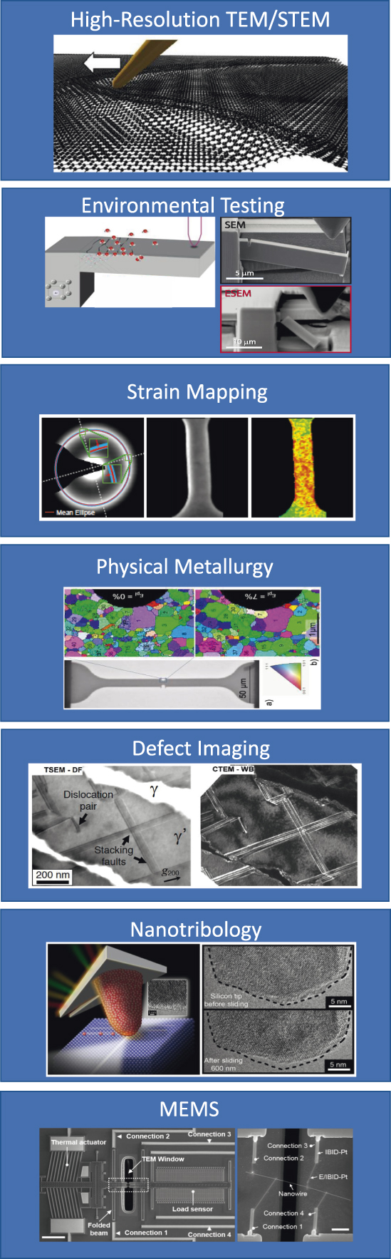
Figure 1. Topical areas related to advanced in situ nanomechanical testing techniques covered in this issue. Note: TEM, transmission electron microsopy; STEM, scanning transmission electron microscopy; MEMS, microelectromechanical systems; ESEM, environmental scanning electron microscopy; CTEM-WB, conventional TEM-weak beam; TSEM-DF, transmission scanning electron microscopy-dark field.
Acknowledgments
A.M. acknowledges support by the Office of Science, Office of Basic Energy Sciences, of the US Department of Energy under Contract No. DE-AC02–05CH11231 within the Mechanical Behavior of Materials (KC 13) Program and at the Molecular Foundry. He also gratefully acknowledges funding from the US Office of Naval Research under Grant Nos. N00014–12–1-0413 and No. N00014–17–1-2283 and STROBE: A National Science Foundation Science and Technology Center under Grant No. DMR 1548924. G.D. acknowledges support by the Max Planck Society, AvH, DFG, DAAD, FFG, COMET K2, and the ERC (Advanced Grant No. 787446-GB-CORRELATE).

Andrew Minor is a professor of materials science and engineering at the University of California, Berkeley, and is also the facility director of the National Center for Electron Microscopy in the Molecular Foundry at the Lawrence Berkeley National Laboratory. He received his BA degree from Yale University in economics and mechanical engineering, and his MS and PhD degrees in materials science and engineering from the University of California, Berkeley. He has co-authored more than 180 publications and presented more than 130 invited talks on topics such as nanomechanics, lightweight alloy development, characterization of soft materials, and in situ transmission electron microscopy technique development. His awards include the LBL Materials Science Division Outstanding Performance Award (2006 and 2010), the American Institute of Mining, Metallurgical, and Petroleum Engineers Robert Lansing Hardy Award from The Minerals, Metals & Materials Society (2012), and the Burton Medal from the Microscopy Society of America (2015). Minor can be reached by email at aminor@berkeley.edu.

Gerhard Dehm is Director of the Max-Planck-Institut für Eisenforschung, Germany, and a professor at the Ruhr-Universität Bochum, Germany. From 2005 to 2012, he was head of the Department of Materials Physics at the Montanuniversität Leoben, Austria, and managing director of the Erich Schmid Institute of Materials Science of the Austrian Academy of Sciences, Austria. He received his degree in materials science from the University of Erlangen-Nuremberg, Germany, and his PhD degree from the University of Stuttgart/ Max-Planck-Institut für Metallforschung, Germany. His more than 300 publications and 170 invited talks cover different topics of materials science, including nano- and micromechanical testing, in situ transmission electron microscopy and x-ray diffraction studies, structure and properties of interfaces, as well as design and stability of thin films and alloys. He has edited a book on in situ electron microscopy, and in 2018, he received an advanced grant from the European Research Council for excellent frontier research. Dehm can be reached by email at dehm@mpie.de.

