


Introduction
Morphological and compositional information at the topmost surface of a specimen is important in the field of materials science and engineering because these parameters strongly affect material properties. The scanning electron microscope (SEM) has been one of the best tools to evaluate the surface structure of materials. At higher electron energies the focused beam spot size becomes smaller, allowing better image resolution; thus SEM images are conventionally recorded at electron accelerating voltages from 10 to 30 kV. High accelerating voltages, however, are unsuitable for obtaining information from the topmost surface because primary electrons then penetrate deep inside the specimen, enlarging the specimen-electron interaction volume and diluting the information related to the topmost surface. Imaging at low accelerating voltages, with a beam of ultra-low landing energies (ULE), defined as a landing energy below 1 keV, is better suited to obtain topmost surface information because the interaction volume and the sampling depth of primary electrons within the specimen becomes small (Figure 1).

Figure 1 Monte Carlo simulations of electron scattering of primary beam electrons in the specimen (material=carbon). (a) Accelerating voltage 1 kV, (b) accelerating voltage 15 kV.
Historically, there have been difficulties with SEM imaging at ULE. One specific problem has been chromatic-aberration enlargement of the electron beam spot size, which causes a degradation of image resolution. To overcome this difficulty in the Hitachi SU8200 series SEM, a beam deceleration technique has been applied along with improvements in the electron source, lenses, and detectors. Specifically, a negative voltage is applied to the specimen to decelerate the primary electrons after the final lens and just before the electron beam interacts with the specimen. As a result, this technique reduces beam aberrations and achieves a small spot size at ULE. High-quality images can be obtained even at landing energies less than 100 eV. Deceleration also reduces sample beam damage and electron dose.
It is sometimes difficult to interpret SEM data at ULE because the signal behavior at ULE does not follow the conventional theory used at the landing energies above 1 keV [Reference Mìllerová1]. Previous studies provide secondary electron (SE) and backscattered electron (BSE) yields as a function of specimen atomic number and of the incident beam energy; these reference data help to interpret the material contrast at ULE [Reference Joy2]. However, the material contrast obtained by an actual instrument does not always follow these earlier results because of the acceptance capability of detectors and the complex phenomena occurring in the specimen chamber: electron scattering at the chamber wall, generating SE3 electrons. In this article, we describe an investigation of material contrast at ULE in an installed SEM and compare the yields obtained to some reference studies.
Materials and Methods
Instrument
Figure 2a shows a general view of the Hitachi SU8230 FE-SEM. The electron source is a cold field emission (CFE) electron gun, which is the best choice for obtaining a small beam spot size at low beam energies. In addition, the CFE source has a small energy spread, which reduces the chromatic aberration. The objective lens in the system is a semi-in-lens type working at a short focal length, which also reduces aberrations. The system configuration can accommodate large specimens—up to 150 mm substrates. The standard vacuum of the specimen chamber is on the order of 10-5 Pa.
Figure 2 General view of the Hitachi SU8230 SEM (left) and schematic of signal detection system using the deceleration mode (right).
The deceleration function is a standard feature of the Hitachi SU8200 series, allowing high-resolution imaging at accelerating voltages less than 1 kV. Figure 3 shows SEM images of mesoporous silica nano particles that are used as catalyst supports or adsorbents. These particles are of amorphous silica, so they are generally susceptible to radiation damage. Therefore, it is necessary to use ULE conditions to reduce sample damage and observe fine structure. In Figure 3 nanopore features about 5 nm in diameter were observed at 500 eV landing energy with no beam damage and no charging.
Figure 3 SE + BSE SEM images of mesoporous silica particles acquired at the following conditions: accelerating voltage = 0.5 kV. Original magnifications (a) 200,000× and (b) 500,000×. Specimen courtesy of Dr. Toshiyuki Yokoi of Tokyo Institute of Technology.
The SU8200 series SEM has three types of SE detectors—the top detector, the upper detector, and the lower Everhart-Thornley detector—which together provide valuable flexibility for imaging. Figure 2b shows a schematic of the signal detection system in the deceleration mode. Electrons with high energy and also a low elevation angle will be detected by the upper detector, providing mainly topographic information. The signal detected by the top detector is controlled by an energy filter called the “top filter.” This works as a high pass filter, allowing only electrons with energy higher than the filtering voltage to be detected. These BSE electrons are converted to SE3s at the converter plate, and the SE3s are detected by the top detector. When the filtering voltage is not applied, SE signals are detected by the top detector mainly in deceleration mode. This is because SEs have low energy and are easily converged by the electrical field and deflected to a high elevation angle into the top detector. When an appropriate combination of landing energy, decelerating voltage, and filtering voltage is applied, SE signals are suppressed and only BSEs that have enough energy to pass through the top filter are detected.
Figure 4 shows SEM images of a composite film comprised of carbon nanotubes (CNTs) on polytetrafluoroethylene (PTFE), which is expected to be used as a protective film for a fuel cell separator film. It is important to measure the distribution of CNTs on the PTFE because the CNT layer affects the conductivity of the composite film. These images were taken by the upper detector and the top detector with the top filter at a landing energy of 0.3 keV. Figure 4a shows the fine structure of the sample observed with the upper detector. In Figure 4b, taken with the top detector, the image contrast between CNTs and the PTFE is greater.
Figure 4 BSE images of CNT/PTFE composite film acquired at the following conditions: accelerating voltage = 0.3 kV, deceleration voltage = 0.5 kV, and filter voltage 0.7 kV. (a) Imaged with upper detector and (b) imaged with top detector. Specimen courtesy of Prof. Yoshiyuki Show of Tokai University.
Specimens
For this article the BSE yield (ηexp) was measured at low accelerating voltages and compared with reference data from the literature. These measurements were made on carbon, silicon, copper, and gold found on the standards block of an electron probe micro analyzer (EPMA). These specimens were suitable for this experiment because of their purity and their flat surface morphologies. The carbon coating film on the standards block was removed by mechanical polishing before it was provided because it could affect the penetration of primary electrons, especially at ULE, and the escape of BSEs and SEs from the surface.
Methods
The backscattered yield was measured on the standard materials at landing energies from 0.2 keV to 1 keV. To compare with reference BSE yields (η ref) listed in reference [Reference Joy2], the experimental BSE yields (η exp) were calculated by the following process. The relationship between experimental signal-to-noise ratio (S/N exp) and theoretical signal-to-noise ratio (S/N theory) is calculated as:
 $$\left( {S/N_{{exp}} } \right)^{2} =k(S/N_{{Theory}} )^{2} ,$$
where k is the detective efficiency estimated using electron trajectory simulations and the SE yield of the conversion plate material [Reference Joy3]. S/N exp can be obtained from:
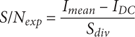 $$S/N_{{exp}} ={{I_{{mean}} {\minus}I_{{DC}} } \over {S_{{div}} }},$$
where I mean is the mean level, I DC is a background level which describes a level when the beam is turned off, and S div is a standard deviation of beam intensity. These parameters were obtained from a histogram of actual SEM images. S/N theory is the signal-to-noise ratio when all the signal is detected, and it can be converted to the number of electrons per pixel (N e) by::
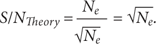 $$S/N_{{Theory}} ={{N_{e} } \over {\sqrt {N_{e} } }}=\sqrt {N_{e} } .$$
By applying the formula (2) and (3) to the formula (1), N e can be calculated by:
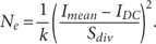 $$N_{e} ={1 \over k}\left( {{{I_{{mean}} {\minus}I_{{DC}} } \over {S_{{div}} }}} \right)^{2} .$$
The η exp values were calculated by::
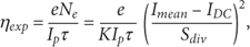 $$\eta _{{exp}} ={{eN_{e} } \over {I_{p} \tau }}={e \over {kI_{p} \tau }}\left( {{{I_{{mean}} {\minus}I_{{DC}} } \over {S_{{div}} }}} \right)^{2} ,$$
where I p is the probe current, e is the electron charge, and τ is the dwell time. The Ip was measured with a faraday cup. The η exp values were compared with the η ref reference data.
Results
Figure 5 shows the comparison of η exp and η ref for (a) carbon, (b) silicon, (c) copper, and (d) gold at the landing energy between 0.2 and 1 keV. In all four materials, the η exp values follow the η ref fairly closely at the lower landing energies. However, there are a few data points that show a deviation from the reference data at the higher landing energy.
Figure 5 Experimental BSE yields (η exp) versus landing energy compared with reference data (η ref) for four elements: (a) carbon, (b) silicon, (c) copper, and (d) gold.
Figure 6 shows the η exp of each material as a function of the landing energy. The η exp values for Cu and Au tend to be higher at the landing energy of around 1 keV and then tend to decrease as the landing energy becomes lower. The η exp of Au is the highest at the landing energy of 1 keV, but it becomes the lowest of the four materials at the landing energy of 0.2 keV. The decrease in the η exp of Cu with beam energy is more gradual than that of Au. In contrast to Cu and Au, the η exp of C and Si tend to be lower at the higher landing energy; these values tend to increase slightly when the landing energy becomes lower. The η exp of Si is higher than that of C at the landing energy between 0.2 to 1 keV, and it is the highest of the four materials at the landing energy of 0.2 keV. The η exp of C is the lowest at the landing energy of 1 keV, but it becomes higher than that of Cu and Au at the landing energy of 0.2 keV.
Figure 6 Experimental BSE yields (η exp) versus landing energy for carbon, silicon, copper, and gold.
To confirm these effects with actual imaging, a test specimen was used consisting of a piece of bare Si substrate next to another piece of Si substrate with a 50 nm thick film of Au deposited on it. Figure 7 shows the BSE images taken at the landing energies of 1 keV and 0.2 keV. At the landing energy of 1 keV, Au appears brighter than Si, whereas at the landing energy of 0.2 keV the contrast was reversed. These images correspond with the graphs shown in Figures 5 and 6.
Figure 7 The reversal of BSE contrast between Au and Si acquired under the following conditions: accelerating voltage was (a) 1 kV, (b) 0.2 kV.
Discussion
The results shown in Figures 5 and 6 correspond reasonably well to the previous studies, except for a few data points. The relationship of η exp versus keV for each material should correspond to the material contrast in the images. The material contrast at the landing energy around 1 keV is proportional to atomic number, but it is not proportional at the lower landing energies. For the lower energies it becomes quite complicated. Gold is the brightest of the four materials at the landing energy of 1 keV. It becomes gradually darker at lower landing energies, and it is the darkest of the four materials at the landing energy of 0.3 keV. Copper is the second brightest of the four materials at the 1 keV landing energy. It also becomes gradually darker at the lower landing energies, and it is the second darkest of the four materials at 0.2 keV. Silicon is the second darkest of the four materials at 1 keV. It becomes slightly brighter at the lowest landing energies and is the brightest of the four materials at 0.2 keV. Carbon is the darkest of the four materials at 1 keV. It becomes slightly brighter at the lower landing energies; it is the second brightest of the four materials at the landing energy of 0.2 keV. These tendencies of reversal have been explained theoretically by the much stronger deviations of elastic Mott cross sections from Rutherford cross sections at ULE [Reference Reimer4]. This effect has been shown experimentally; at very low primary electron energies the BSE yields of heavier materials tend to decrease, and the BSE yields of lighter materials tend to increase [Reference Mìllerová5–Reference El Gomati6].
There are several possible causes of the deviations of the experimental values from the reference data (Figure 5). One may be due to the difference in the sample state because the BSE yield is sensitively affected by factors such as cleanliness and flatness. There might be a little bit of contamination on the sample surface due to a hydrocarbon film (re)deposited by the electron beam, even though the vacuum in the chamber was very good, which is on the order of 10-5 Pa, and the samples were carefully handled. In addition, instrumental factors such as the acceptance capabilities of the detector could affect the results. The complex phenomena occurring inside the chamber such as the generation of SE3 could affect the signal intensity as well.
Conclusion
The material contrast at the landing energy higher at 1 keV is proportional to atomic number as expected, but it is not proportional to the atomic number at the landing energy of 0.2 keV. At the latter landing energy, C and Si were brighter than Cu and Au. The η exp values nearly correspond to the η ref, below about 0.5 keV, but there are a few experimental data points near 1 keV that are higher than the η ref by a factor of two. Possible causes of the deviation include differences in sample state, contamination, the acceptance capabilities of the detector, and/or the complex phenomena occurring inside the specimen chamber.

