Hostname: page-component-8448b6f56d-c47g7 Total loading time: 0 Render date: 2024-04-23T05:32:00.563Z Has data issue: false hasContentIssue false

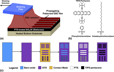
Selective solution shearing deposition of high performance TIPS-pentacene polymorphs through chemical patterning

Published online by Cambridge University Press:  31 October 2014

Gaurav Giri
Affiliation:
Department of Chemical Engineering, Stanford University, Stanford, California 94305, USA
Eric Miller
Affiliation:
Department of Chemical Engineering, Stanford University, Stanford, California 94305, USA
Zhenan Bao*
Affiliation:
Department of Chemical Engineering, Stanford University, Stanford, California 94305, USA
*
a)Address all correspondence to this author. e-mail: zbao@stanford.edu
Get access

Abstract

Methods for the solution deposition of organic semiconductors (OSCs) show great potential for the production of large-area, inexpensive, and flexible organic electronics. A solution deposition method called solution shearing has consistently been shown to yield thin film transistors with improved performance over those created via other solution-based approaches. However, the need for discrete, electronically isolated devices requires the parallel development of a facile means of pattern definition compatible with the solution shearing process. In our work, we use a simple chemical prepatterning method to enable the solution shearing deposition of the small molecule OSC TIPS-pentacene on substrates with feature sizes as small as 100 µm. Grazing incidence x-ray diffraction (GIXD) was also used to confirm the existence of high performance TIPS-pentacene polymorphs in the patterned thin films. Mobilities as high as 1.13 cm2 V−1 s−1 were obtained on 400 µm wide patterns by depositing a high-performance, metastable polymorph of TIPS-pentacene.

Type
Invited Feature Papers
Copyright
Copyright © Materials Research Society 2014 

Access options

Get access to the full version of this content by using one of the access options below. (Log in options will check for institutional or personal access. Content may require purchase if you do not have access.)

References

REFERENCES

Klauk, H.: Organic Electronics: Materials, Manufacturing, and Applications (Wiley-VCH, Weinheim, 2006).CrossRefGoogle Scholar
Forrest, S.R.: The road to high efficiency organic light emitting devices. Org. Electron. 4(2), 45 (2003).Google Scholar
Kelley, T.W., Baude, P.F., Gerlach, C., Ender, D.E., Muyres, D., Haase, M.A., Vogel, D.E., and Theiss, S.D.: Recent progress in organic electronics: Materials, devices, and processes. Chem. Mater. 16(23), 4413 (2004).Google Scholar
Berggren, M., Nilsson, D., and Robinson, N.D.: Organic materials for printed electronics. Nat. Mater. 6(1), 3 (2007).CrossRefGoogle ScholarPubMed
Malliaras, G. and Friend, R.: An organic electronics primer. Phys. Today 58, 53 (2005).CrossRefGoogle Scholar
Chua, L-L., Zaumseil, J., Chang, J-F., Ou, E.C-W., Ho, P.K-H., Sirringhaus, H., and Friend, R.H.: General observation of n-type field-effect behaviour in organic semiconductors. Nature 434(7030), 194 (2005).Google Scholar
Dimitrakopoulos, C.D. and Malenfant, P.R.L.: Organic thin film transistors for large area electronics. Adv. Mater. 14(2), 99 (2002).Google Scholar
Park, S.K., Jackson, T.N., Anthony, J.E., and Mourey, D.A.: High mobility solution processed 6, 13-bis (triisopropyl-silylethynyl) pentacene organic thin film transistors. Appl. Phys. Lett. 91, 063514 (2007).Google Scholar
Klauk, H., Halik, M., Zschieschang, U., Schmid, G., Radlik, W., and Weber, W.: High-mobility polymer gate dielectric pentacene thin film transistors. J. Appl. Phys. 92(9), 5259 (2002).Google Scholar
Jurchescu, O.D., Baas, J., and Palstra, T.: Effect of impurities on the mobility of single crystal pentacene. Appl. Phys. Lett. 84(16), 3061 (2004).Google Scholar
Podzorov, V., Pudalov, V., and Gershenson, M.: Field-effect transistors on rubrene single crystals with parylene gate insulator. Appl. Phys. Lett. 82(11), 1739 (2003).Google Scholar
Sokolov, A.N., Atahan-Evrenk, S., Mondal, R., Akkerman, H.B., Sánchez-Carrera, R.S., Granados-Focil, S., Schrier, J., Mannsfeld, S.C., Zoombelt, A.P., Bao, Z., and Aspuru-Guzik, A.: From computational discovery to experimental characterization of a high hole mobility organic crystal. Nat. Commun. 2, 437 (2011).Google Scholar
Minemawari, H., Yamada, T., Matsui, H., Tsutsumi, J.Y., Haas, S., Chiba, R., Kumai, R., and Hasegawa, T.: Inkjet printing of single-crystal films. Nature 475(7356), 364 (2011).Google Scholar
Izawa, T., Miyazaki, E., and Takimiya, K.: Molecular ordering of high-performance soluble molecular semiconductors and re-evaluation of their field-effect transistor characteristics. Adv. Mater. 20(18), 3388 (2008).CrossRefGoogle Scholar
Park, J., Lee, S., and Lee, H.H.: High-mobility polymer thin-film transistors fabricated by solvent-assisted drop-casting. Org. Electron. 7(5), 256 (2006).Google Scholar
Chang, J-F., Sun, B., Breiby, D.W., Nielsen, M.M., Sölling, T.I., Giles, M., McCulloch, I., and Sirringhaus, H.: Enhanced mobility of poly (3-hexylthiophene) transistors by spin-coating from high-boiling-point solvents. Chem. Mater. 16(23), 4772 (2004).Google Scholar
DeLongchamp, D.M., Kline, R.J., Jung, Y., Germack, D.S., Lin, E.K., Moad, A.J., Richter, L.J., Toney, M.F., Heeney, M., and McCulloch, I.: Controlling the orientation of terraced nanoscale “ribbons” of a poly (thiophene) semiconductor. ACS Nano 3(4), 780 (2009).CrossRefGoogle ScholarPubMed
Schilinsky, P., Waldauf, C., and Brabec, C.J.: Performance analysis of printed bulk heterojunction solar cells. Adv. Funct. Mater. 16(13), 1669 (2006).Google Scholar
Wengeler, L., Schmidt-Hansberg, B., Peters, K., Scharfer, P., and Schabel, W.: Investigations on knife and slot die coating and processing of polymer nanoparticle films for hybrid polymer solar cells. Chem. Eng. Process. 50(5), 478 (2011).CrossRefGoogle Scholar
de Gans, B.J., Duineveld, P.C., and Schubert, U.S.: Inkjet printing of polymers: State of the art and future developments. Adv. Mater. 16(3), 203 (2004).Google Scholar
Pisula, W., Menon, A., Stepputat, M., Lieberwirth, I., Kolb, U., Tracz, A., Sirringhaus, H., Pakula, T., and Müllen, K.: A zone-casting technique for device fabrication of field-effect transistors based on discotic hexa-peri-hexabenzocoronene. Adv. Mater. 17(6), 684 (2005).Google Scholar
Tracz, A., Makowski, T., Masirek, S., Pisula, W., and Geerts, Y.: Macroscopically aligned films of discotic phthalocyanine by zone casting. Nanotechnology 18(48), 485303 (2007).CrossRefGoogle Scholar
Becerril, H.A., Roberts, M.E., Liu, Z., Locklin, J., and Bao, Z.: High-performance organic thin-film transistors through solution-sheared deposition of small-molecule organic semiconductors. Adv. Mater. 20(13), 2588 (2008).Google Scholar
Liu, Z., Becerril, H.A., Roberts, M.E., Nishi, Y., and Bao, Z.: Experimental study and statistical analysis of solution-shearing processed organic transistors based on an asymmetric small-molecule semiconductor. IEEE Trans. Electron Devices 56(2), 176 (2009).Google Scholar
Giri, G., Verploegen, E., Mannsfeld, S.C., Atahan-Evrenk, S., Lee, S.Y., Becerril, H.A., Aspuru-Guzik, A., Toney, M.F., and Bao, Z.: Tuning charge transport in solution-sheared organic semiconductors using lattice strain. Nature 480(7378), 504 (2011).CrossRefGoogle ScholarPubMed
Diao, Y., Tee, B.C.K., Giri, G., Xu, J., Kim, D.H., Becerril, H.A., Stoltenberg, R.M., Lee, T.H., Xue, G., Mannsfeld, S.C.B., and Bao, Z.: Solution coating of large-area organic semiconductor thin films with aligned single-crystalline domains. Nat. Mater. 12(7), 665 (2013).Google Scholar
Dickey, K.C., Subramanian, S., Anthony, J.E., Han, L-H., Chen, S., and Loo, Y-L.: Large-area patterning of a solution-processable organic semiconductor to reduce parasitic leakage and off currents in thin-film transistors. Appl. Phys. Lett. 90(24), 244103 (2007).Google Scholar
Kymissis, I., Dimitrakopoulos, C.D., and Purushothaman, S.: Patterning pentacene organic thin film transistors. J. Vac. Sci. Technol., B: Microelectron. Nanometer Struct. 20(3), 956 (2002).Google Scholar
Ling, M.M. and Bao, Z.: Thin film deposition, patterning, and printing in organic thin film transistors. Chem. Mater. 16(23), 4824 (2004).Google Scholar
Briseno, A.L., Mannsfeld, S.C.B., Ling, M.M., Liu, S., Tseng, R.J., Reese, C., Roberts, M.E., Yang, Y., Wudl, F., and Bao, Z.: Patterning organic single-crystal transistor arrays. Nature 444(7121), 913 (2006).Google Scholar
Mannsfeld, S.C., Sharei, A., Liu, S., Roberts, M.E., McCulloch, I., Heeney, M., and Bao, Z.: Highly efficient patterning of organic single-crystal transistors from the solution phase. Adv. Mater. 20(21), 4044 (2008).Google Scholar
Briseno, A.L., Mannsfeld, S.C., Reese, C., Hancock, J.M., Xiong, Y., Jenekhe, S.A., Bao, Z., and Xia, Y.: Perylenediimide nanowires and their use in fabricating field-effect transistors and complementary inverters. Nano Lett. 7(9), 2847 (2007).Google Scholar
Oh, J.H., Lee, H.W., Mannsfeld, S., Stoltenberg, R.M., Jung, E., Jin, Y.W., Kim, J.M., Yoo, J-B., and Bao, Z.: Solution-processed, high-performance n-channel organic microwire transistors. Proc. Natl. Acad. Sci. U. S. A. 106(15), 6065 (2009).Google Scholar
DeFranco, J.A., Schmidt, B.S., Lipson, M., and Malliaras, G.G.: Photolithographic patterning of organic electronic materials. Org. Electron. 7(1), 22 (2006).Google Scholar
Nakayama, K., Hirose, Y., Soeda, J., Yoshizumi, M., Uemura, T., Uno, M., Li, W., Kang, M.J., Yamagishi, M., Okada, Y., Miyazaki, E., Nakazawa, Y., Nakao, A., Takimiya, K., and Takeya, J.: Patternable solution-crystallized organic transistors with high charge carrier mobility. Adv. Mater. 23(14), 1626 (2011).CrossRefGoogle ScholarPubMed
Akkerman, H.B., Chang, A.C., Verploegen, E., Bettinger, C.J., Toney, M.F., and Bao, Z.: Fabrication of organic semiconductor crystalline thin films and crystals from solution by confined crystallization. Org. Electron. 13(2), 235 (2012).Google Scholar
Kang, B., Min, H., Seo, U., Lee, J., Park, N., Cho, K., and Lee, H.S.: Directly drawn organic transistors by capillary pen: A new facile patterning method using capillary action for soluble organic materials. Adv. Mater. 25(30), 4117 (2013).Google Scholar
Jo, P.S., Vailionis, A., Park, Y.M., and Salleo, A.: Scalable fabrication of strongly textured organic semiconductor micropatterns by capillary force lithography. Adv. Mater. 24(24), 3269 (2012).Google Scholar
Dickey, K., Anthony, J.E., and Loo, Y-L.: Improving organic thin-film transistor performance through solvent-vapor annealing of solution processable triethylsilylethynyl anthradithiophene. Adv. Mater. 18, 1721 (2006).Google Scholar
Goto, O., Tomiya, S., Murakami, Y., Shinozaki, A., Toda, A., Kasahara, J., and Hobara, D.: Organic single-crystal arrays from solution-phase growth using micropattern with nucleation control region. Adv. Mater. 24(8), 1117 (2012).CrossRefGoogle ScholarPubMed
Ward, J.W., Loth, M.A., Kline, R.J., Coll, M., Ocal, C., Anthony, J.E., and Jurchescu, O.D.: Tailored interfaces for self-patterning organic thin-film transistors. J. Mater. Chem. 22(36), 19047 (2012).Google Scholar
Minari, T., Liu, C., Kano, M., and Tsukagoshi, K.: Controlled self-assembly of organic semiconductors for solution-based fabrication of organic field-effect transistors. Adv. Mater. 24(2), 299 (2012).CrossRefGoogle ScholarPubMed
Li, Y., Liu, C., Kumatani, A., Darmawan, P., Minari, T., and Tsukagoshi, K.: Large plate-like organic crystals from direct spin-coating for solution-processed field-effect transistor arrays with high uniformity. Org. Electron. 13(2), 264 (2012).Google Scholar
Li, H., Tee, B.C.K., Giri, G., Chung, J.W., Lee, S.Y., and Bao, Z.: High-performance transistors and complementary inverters based on solution-grown aligned organic single-crystals. Adv. Mater. 24(19), 2588 (2012).Google Scholar
Park, S.K., Mourey, D.A., Subramanian, S., Anthony, J.E., and Jackson, T.N.: Non-relief-pattern lithography patterning of solution processed organic semiconductors. Adv. Mater. 20(21), 4145 (2008).CrossRefGoogle Scholar
Giri, G., Park, S., Vosgueritchian, M., Shulaker, M.M., and Bao, Z.: High-mobility, aligned crystalline domains of TIPS-pentacene with metastable polymorphs through lateral confinement of crystal growth. Adv. Mater. 26(3), 487 (2014).Google Scholar
Ito, Y., Virkar, A.A., Mannsfeld, S., Oh, J.H., Toney, M., Locklin, J., and Bao, Z.: Crystalline ultrasmooth self-assembled monolayers of alkylsilanes for organic field-effect transistors. J. Am. Chem. Soc. 131(26), 9396 (2009).Google Scholar
Mannsfeld, S.C., Tang, M.L., and Bao, Z.: Thin film structure of triisopropylsilylethynyl-functionalized pentacene and tetraceno [2, 3-b] thiophene from grazing incidence x-ray diffraction. Adv. Mater. 23(1), 127 (2011).Google Scholar