


Introduction
Scanning transmission electron microscopy (STEM) is a method mostly used to investigate the nanostructure of very thin specimens (<100 nm) (Nellist et al., Reference Nellist, Chisholm, Dellby, Krivanek, Murfitt, Szilagyi, Lupini, Borisevich, Sides and Pennycook2004; Krivanek et al., Reference Krivanek, Chisholm, Nicolosi, Pennycook, Corbin, Dellby, Murfitt, Own, Szilagyi, Oxley, Pantelides and Pennycook2010), whereby an annular dark field (ADF) detector collects the electrons scattered into a certain angular range. The thickness of the specimen is usually prepared to be thinner than the mean-free-path-length for elastic scattering of the electrons in the material. However, there is a range of research questions, where it is of interest to image through thicker samples. Examples are STEM experiments in liquid (de Jonge & Ross, Reference de Jonge and Ross2011), thick polymer films (Loos et al., Reference Loos, Sourty, Lu, Freitag, Tang and Wall2009), and analytical electron microscopy of biological specimens (Colliex, et al., Reference Colliex, Jeanguillaume and Mory1984; Engel & Colliex, Reference Engel and Colliex1993; Sousa et al., Reference Sousa, Aronova, Kim, Dorward, Zhang and Leapman2007; Engel, Reference Engel2009). In particular for three-dimensional (3D) STEM tomography, the capability of STEM to obtain excellent resolution through micrometers-thick sections of cellular material is of advantage (Yakushevska et al., Reference Yakushevska, Lebbink, Geerts, Spek, van Donselaar, Jansen, Humbel, Post, Verkleij and Koster2007; Aoyama et al., Reference Aoyama, Takagi, Hirase and Miyazawa2008; Hohmann-Marriott, et al., Reference Hohmann-Marriott, Sousa, Azari, Glushakova, Zhang, Zimmerberg and Leapman2009; Biskupek et al., Reference Biskupek, Leschner, Walther and Kaiser2010; Wolf et al., Reference Wolf, Houben and Elbaum2014). STEM tomography is also frequently used in materials science (Kuebel et al., Reference Kuebel, Voigt, Schoenmakers, Otten, Su, Lee, Carlsson and Bradley2005). The scanning capabilities of STEM can easily be combined with analytical methods (Midgley & Dunin-Borkowski, Reference Midgley and Dunin-Borkowski2009) such as energy dispersive X-ray analysis (Lepinay et al., Reference Lepinay, Lorut, Pantel and Epicier2013), and also allow alternative acquisition strategies to obtain 3D information of thick specimens (Frigo et al., Reference Frigo, Levine and Zaluzec2002; Behan et al., Reference Behan, Cosgriff, Kirkland and Nellist2009; Dahmen et al., Reference Dahmen, Baudoin, Lupini, Kubel, Slusallek and de Jonge2014). Finally, STEM tomography in scanning electron microscopy (SEM) is possible, allowing a maximal sample space for experiments (Jornsanoh et al., Reference Jornsanoh, Thollet, Ferreira, Masenelli-Varlot, Gauthier and Bogner2011).
But despite this wide range of applications, the spatial resolution achieved for thick specimens is not yet fully understood. For thin specimens, the spatial resolution is given by the point spread function of the focused electron probe in vacuum, which is well known and is of a lateral size of 0.1 nm for modern spherical aberration-corrected STEM instruments. The resolution for a thick layer is more complex to calculate as it depends on both the microscope settings and sample properties and geometry (Colliex, et al. Reference Colliex, Jeanguillaume and Mory1984; Reimer & Kohl, Reference Reimer and Kohl2008; de Jonge et al., 2010 Reference de Jonge, Poirier-Demers, Demers, Peckys and Drouinb ). The highest resolution is achieved for objects in the top layer of the sample with respect to a downward traveling electron beam, for example, gold nanoparticles (AuNPs) on a water layer (de Jonge et al., 2010 Reference de Jonge, Poirier-Demers, Demers, Peckys and Drouinb ). Scanning objects with the electron beam at or close to the top surface is only influenced a little by the material above the object plane, and an optimal spatial resolution can be achieved as there are no image forming lenses below the sample. The situation is different when the electron beam has to penetrate through a considerable thickness of matter to generate contrast at objects positioned at lower vertical positions or even at the bottom of the sample matrix. Under these conditions, in particular for matrix thicknesses beyond the mean-free-path-length of the electron probe, the scattering of the electron beam in the matrix leads to a significant broadening of the electron beam. The reduction of the resolution for imaging objects below the sample due to beam broadening by electron–sample interactions is the so called top-bottom-effect (Reimer & Kohl, Reference Reimer and Kohl2008). The broadening has been described by an analytical equation matching experimental data within a factor of two (Reimer & Kohl, Reference Reimer and Kohl2008), and several other analytical models exist in literature (Demers et al., Reference Demers, Ramachandra, Drouin and de Jonge2012) (e.g., Goldstein, Reference Goldstein1979; Rez, Reference Rez1983; Gauvin & Rudinsky, Reference Gauvin and Rudinsky2016). But these models substantially differ in the quantitative numbers, the resolution is typically calculated below the sample only, and an analytical model is not available to describe the influence of beam broadening on the resolution obtained for objects within the sample and not at the bottom of the sample. Crucial for the analytical model is a description of multiple scattering. An alternative and precise approach to estimate the beam broadening is to use Monte Carlo simulations providing quantitative numbers (Hyun et al., Reference Hyun, Ercius and Muller2008; Sousa et al., Reference Sousa, Hohmann-Marriott, Zhang and Leapman2009; Demers et al., Reference Demers, Poirier-Demers, Drouin and de Jonge2010). But this is not always desirable, as it is time-consuming to vary parameters to explore the most optimal conditions for an experiment.
Here, we provide a theoretical and experimental framework for determining the influence of probe broadening on the lateral resolution of ADF STEM as function of the vertical location, z, of the object within the sample matrix. As an example, we will consider an Al matrix of several hundreds of nanometers thickness in which AuNPs are embedded. Several different samples will be examined with STEM in which z and the sample thickness, t, are varied. The theoretical model will use the standard equations for elastic electron scattering in a specimen, and different analytical models for beam broadening will be evaluated. In particular, we show that multiple scattering needs to be taken into account.
Materials and Methods
Sample Preparation
Silicon microchips with silicon nitride (SiN) windows of dimensions of 160×400 µm2 and 0.05 µm thickness (DENSsolutions, Delft, The Netherlands) were used as sample supports. The microchips were cleaned in acetone (high-performance liquid chromatography [HPLC] grade), and then in ethanol (HPLC grade), followed by a treatment in an Argon/Air-plasma using a procedure described elsewhere (Ring et al., Reference Ring, Peckys, Dukes, Baudoin and de Jonge2011). Multiple layers of aluminum were deposited onto the microchips by means of physical vapor deposition. The physical vapor deposition system (Kurt J Lesker Company, Jefferson Hills, PA, USA) was operated in the magnetron direct current sputter mode at pressure of 5 mTorr of argon and a process power of 100 W. The aluminum target (Kurt J Lesker, >99.99 mass% purity) was rotated at 10 rpm. Spherical AuNPs were applied on the surface of the sample after the deposition of different numbers of aluminum layers. Each layer had a thickness of ~0.15 µm. A suspension of AuNPs was prepared by mixing suspensions of spherical 5 and 10 nm AuNPs (EM.GC5 and EMGC10; BBInternational, Cardiff, UK).
Three different types of microchips were prepared with four Al layers. On microchip 1, the AuNP suspension was placed, dried out, and then washed with water after the first layer of aluminum was deposited. For microchips 2 and 3, the AuNP suspension was deposited onto the second and third layer of aluminum, respectively. Afterwards, further layers of aluminum were deposited giving a total of four Al layers on all three microchips. A fourth microchip was prepared with two additional Al layers, and the AuNPs were deposited onto the second layer of Al. Au nanorods of 30 nm diameter were placed on the top aluminum layer and on the SiN membrane (opposite site) afterwards. These nanorods were used as fiducials, marking the top and the bottom of the sample as needed to determine the total thickness of the specimen, and to measure the vertical position of the AuNP layers within the aluminum matrix. In addition, AuNPs of 5 nm diameter were placed on top of sample 1.
STEM
A probe C S -corrected (ARM200CF; JEOL, Tokyo, Japan) transmission electron microscope equipped with a cold field emission gun was used for the investigations. The microscope was operated at 200 kV acceleration voltage in STEM mode. Micrographs were acquired at an electron probe current of 180 pA, and a pixel dwell time of 19 µs. A 30-µm aperture was used resulting in a beam convergence semi-angle of α=19.8 mrad. The inner detector opening semi-angle was ~43 mrad. This detector angle refers to the opening through which current may pass as needed for current measurements using the phosphor screen. The semi-angle measuring the active area of the detector collecting the ADF signal was larger, β=68 mrad (see Fig. 1). The outer collecting semi-angle amounted to 280 mrad. The electron dose introduced per image varied between 1,200 and 4,600 e−/Å2 depending on the magnification. Note that this commonly used term electron dose in fact means electron density. The image size was 1,024×1,024 pixels. According to the manufacturer, the minimum probe size of the focused electron beam under the chosen conditions (probe size selector, condenser lens aperture) is of the order of 0.12 nm. The aluminum coated silicon microchips were mounted in a standard single tilt holder. Overview images with a on screen magnification of 100,000× at the different positions were acquired at x-axis tilting angles of 0° and 10°, respectively. These micrographs were used to determine the thickness of the support material, and also the vertical depth of the 5–10-nm diameter AuNPs by analyzing the lateral displacement of the particles at the different tilting angles. Additional micrographs were acquired focusing on the AuNPs at different vertical positions (nanorods on top and at the bottom, AuNPs within the aluminum).
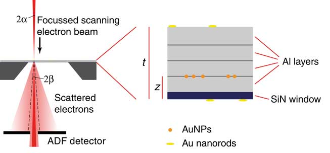
Figure 1 Schematic of the experimental setup. The sample was studied with scanning transmission electron microscopy (STEM) using the annular dark field (ADF) detector. The opening semi-angles of the electron beam α and of the ADF detector β are indicated. The active area of the detector is smaller than the hole through which the non-detected current passes. The dimensions are not to scale but the relative angles match the experiment. A silicon microchip with an electron transparent silicon nitride (SiN) membrane window was coated with multiple Al layers. Spherical Au nanoparticles (AuNPs) of diameters between 5 and 10 nm were deposited between two Al layers of aluminum at vertical location z measured with respect to the bottom of the SiN membrane window. Four different samples were made in which the layer with AuNPs was at a different z. Au nanorods were placed as fiducial markers at the top and the bottom of the sample of total thickness t.
Data Analysis
For the determination of the beam broadening, intensity profiles over AuNPs between Al layers were measured in ImageJ (NIH) and evaluated by means of a python script. The profiles were smoothed using a moving average over 5 data points and normalized to 1. The FWHM and the r 25–75 intensity were determined.
Monte Carlo Simulation of Intensity Profiles
Monte Carlo STEM lateral line scans of AuNPs inside an Al matrix were simulated and compared with the experimental data and theoretical models to study the effect of the vertical position of the AuNPs on the spatial resolution. The Monte Carlo simulations were carried out using the program named Casino (Demers et al., Reference Demers, Poirier-Demers, Drouin and de Jonge2010, Reference Demers, Poirier-Demers, Couture, Joly, Guilmain, de Jonge and Drouin2011). The software included the elastic scattering of electrons and positrons by atoms elastic electron scattering cross section (Salvat et al., Reference Salvat, Jablonski and Powell2007), Poisson noise characteristics of the electron source, and the electron optics of the STEM (ADF detector and scanning of a focused electron beam). The simulation of STEM images was calibrated using experimental data (Demers et al., Reference Demers, Poirier-Demers, Drouin and de Jonge2010; de Jonge et al., 2010 Reference de Jonge, Poirier-Demers, Demers, Peckys and Drouinb ). The vertical position z of the AuNPs of 10 nm diameter was varied between 0 and 600 nm with a 50-nm step in the 0.6-µm thick sample. In each line scan, the lateral probe position was varied between −25 and 25 nm with a step size of 0.1 nm. The accelerating voltage was 200 kV with a probe size of 0.12 nm. For all simulations, the beam was focused at the vertical position of the AuNP. The simulations were obtained for ADF detector inner and outer semi-angles of 68 and 280 mrad, respectively. The simulations were conducted with both the same electron dose as the experimental data and an electron dose 100 times greater than the experimental dose. The simulated data was smoothed using a moving average over five data point and normalized to 1 to accurately calculate the r 25–75 for each line scan.
Calculation of Signal Profiles
Imaging a spherical particle was mathematically described in two dimensions by the convolution of an approximately circular shape with a Gaussian beam shape (using Mathematica 8; Wolfram Research, Oxfordshire, UK). The standard convolution integral did not work for the equation of a circle y=√(1−x 2) and, therefore, the circle was approximated by the 6th order Taylor approximation for −1<x<1 and 0 otherwise. As measures of signal profiles of line scans over an object, the edge width corresponding to a rise in signal of 25–75% of the maximum intensity r 25 was used. Also, the diameter of a signal peak containing 50% of the current d 50 was used. For theoretical calculations, these measures were calculated from signal profiles (using Mathematica 8), using a Gaussian profile or using a Gaussian profile convoluted with a circle.
Theory
Electron Scattering Cross Sections
The scattering of electrons is a statistical process that depends on the scattering cross sections of the materials through which the electrons penetrate. For ADF STEM, the signal in the detector is dominated by elastic scattering. It is calculated via the differential cross section for elastic scattering dσ el/dΩ assuming a simple screened Rutherford scattering model based on a Wentzel potential (Reimer & Kohl, Reference Reimer and Kohl2008):
 $${{d\sigma _{{el}} } \over {d\Omega }}\,{\equals}\,{{4Z^{{2/3}} \,\alpha ^{2} _{H} \left( {1{\plus}E/E_{0} } \right)^{2} } \over {{\rm l{\plus}(}\theta {\rm /}\theta _{{\rm 0}} {\rm )}^{{\rm 2}} }},$$
with scattering angle θ, Bohr radius a H , atomic number Z, electron energy E, and the relativistic wavelength of the electron:
 $$\lambda \,{\equals}\,{{hc} \over {\sqrt {2EE_{0} {\plus}E^{2} } }},$$
with Planck’s constant h, the speed of light c, and the rest energy given by:
 $$E_{0} \,{\equals}\,m_{0} c^{2} ,$$
with the rest mass of the electron m 0. The characteristic angle is given by:
 $$\theta _{0} \,{\equals}\,{{\lambda Z^{{1/3}} } \over {2\pi \alpha _{H} }}$$
To calculate the number of electrons received by the ADF detector, dσ el/dΩ is integrated over θ from β to π, yielding the differential cross section σ el(β):
 $$\sigma _{{el}} (\beta )\,{\equals}\,{{Z^{{4/3}} \,\lambda ^{2} \,\left( {1{\plus}E/E_{0} } \right)^{2} } \over \pi }\,{1 \over {1{\plus}\left( {\beta /\theta _{0} } \right)^{2} }},$$
with the detector opening semi-angle β. The outer acceptance angle of the ADF detector is neglected as only a very small fraction of the current is scattered into larger angles. Angular deviation caused by inelastic scattering is typically negligible, so that the total partial cross section equals σ(β)=σ el (β).
Mean-Free-Path-Length
The signal obtained with ADF STEM is calculated from the amount of electrons N scattered by an angle β or larger (Reimer & Kohl, Reference Reimer and Kohl2008):
 $${N \over {N_{0} }}\,{\equals}\,1{\minus}e^{{{\minus}t/l(\beta )}} ,$$
with N 0 the number of incident electrons, t the thickness of the material, and l(β) the mean-free-path length for elastic scattering:
 $$l\left( \beta \right)\,{\equals}\,{W \over {\sigma (\beta )\,\rho N_{{\rm A}} }},$$
with mass density ρ, the atomic weight W and Avogadro’s number N A.
ADF Signal
Considering the sample containing AuNPs embedded in a thin Al layer, the signal in the ADF detector N signal is given by (Reimer & Kohl, Reference Reimer and Kohl2008; de Jonge et al., Reference de Jonge, Peckys, Kremers and Piston2009):
 $$N_{{{\rm signal}}} \,{\equals}\,N_{0} \left\{ {1{\minus}{\rm exp}\left[ {{\minus}\left( {{d \over {l_{{{\rm Au}}} }}{\plus}{{t{\minus}d} \over {l_{{{\rm Al}}} }}} \right)} \right]} \right\},$$
with l Au and l Al, the mean free path lengths in Au and Al, respectively, the diameter of the nanoparticle d, and the sample thickness t. The scattering in the SiN membrane can be approximated by scattering in Al and thus does not need to be accounted for separately, as their mean free path lengths are almost equal. For nanoparticles in thin samples, multiple scattering is also neglected. A background signal N bkg is obtained in areas not containing nanoparticles:
 $$N_{{{\rm bkg}}} \,{\equals}\,N_{0} \left\{ {1{\minus}{\rm exp}\left( {{\minus}{t \over {l_{{{\rm Al}}} }}} \right)} \right\}.$$
Note that equation (9) can be resolved to obtain t as function of the ratio of N 0 and N bkg, which was used to determine the sample thickness.
Signal-to-noise ratio (SNR)-Limited Resolution
Contrast in the image originates from comparing pixels representing sample locations with nanoparticles with pixels at the background. Assuming a thick Al layer so that the background signal is larger than the signal of the nanoparticles alone, and the pixels at the location of a nanoparticle are thus only minimally larger than the background, the SNR (equivalent to the signal-to-background ratio in this case) becomes:
 $${\rm SNR}\,{\equals}\,{{N_{{{\rm signal}}} {\minus}N_{{{\rm bkg}}} } \over {\sqrt {N_{{{\rm bkg}}} } }}\geq 3.$$
According to the Rose criterion (Rose, Reference Rose1948), the particle is detectable if the SNR ≥3. Equation (10) was solved to obtain the SNR-limited spatial resolution d SNR:
 $$d_{{{\rm SNR}}} \,{\equals}\,{{l_{{{\rm Al}}} l_{{{\rm Au}}} } \over {l_{{{\rm Au}}} {\minus}l_{{{\rm Al}}} }}\left( {{\rm In}\left\{ {{\minus}3\sqrt \left( {1{\minus}{\rm e}^{{{\minus}{t \over {l_{{{\rm Al}}} }}}} } \right) {/{\it N}_{0} {\plus}} {\rm e}^{{{\minus}{t \over {l_{{{\rm Al}}} }}}} } \right\}{\plus}{t \over {l_{{{\rm Al}}} }}} \right).$$
This factor determines the resolution for nanoparticles in the top layer of a specimen with respect to a downward traveling electron beam (Schuh & de Jonge, Reference Schuh and de Jonge2014)
Probe Broadening
When an electron beam propagates through a sample, an increasing number of electrons are scattered the deeper the beam passes through the material, and a focused electron probe in STEM is thus broadened. Probe broadening becomes the resolution-limiting factor for nanoparticles deeper in the sample. Several approaches to calculate probe broadening will be described in the following. A pencil-shaped electron beam is considered.
(i) Single scattering event. The broadening is considered to occur as a single scattering event in the middle of the sample at depth t/2 (Goldstein, Reference Goldstein1979), and one examines the cone of scattered electrons containing a certain fraction of the current. The size of the broadened probe d blur follows from:
 $$d_{{{\rm blur}}} \,{\equals}\,2\beta _{{{\rm max}}} \,t/2,$$
with the semi-angle outlining the scattered cone β max. The original equation was derived with the purpose to calculate the spatial resolution of X-ray analysis in SEM, and intended to calculate the size of the area from which X-rays originated. For this reason, the fraction of the current was set to 90%. Several approximations were made to obtain the following analytical expression:
 $$d_{{{\rm blur}}} \,{\equals}\,6.25{\times}10^{5} \,{Z \over E}\,\sqrt {{\rho \over W}} \,t^{{3/2}} ,$$
with length units traditionally given in centimeters. However, this equation gives a too large estimate of probe broadening when imaging is considered. Much of the broadening leads to a background signal due to beam tails originating from larger scattering angles. The presence of beam tails would still allow imaging with high resolution using the unperturbed fraction of the probe but with a lower SNR (de Jonge et al., 2010 Reference de Jonge, Poirier-Demers, Demers, Peckys and Drouinb ; Demers et al., Reference Demers, Ramachandra, Drouin and de Jonge2012).
(ii) Approximate analytical model, including multiple scattering. An approximate analytical model was developed using the multiple-scattering theory proposed by Bothe (Reference Bothe1951) and resolved for probe broadening (Reimer & Kohl, Reference Reimer and Kohl2008):
 $$d_{{{\rm blur}}} {\equals}{{\lambda ^{2} } \over {2\pi \alpha _{H} }}\,t^{{1.5}} \,\sqrt {{{N_{{A\rho }} } \over {3\pi W}}} \,Z\left( {1{\plus}E/E_{0} } \right).$$
Here, the blurring diameter is measured from the intensity distribution across an edge imaged with a scanning probe, which defines the width r 25–75 in which the signal rises from 25% to 75% of the maximum intensity. The equation matched experimental results based on measuring the FWHM (de Jonge et al., 2010 Reference de Jonge, Poirier-Demers, Demers, Peckys and Drouinb ). Yet, this equation also has a limited precision and was shown to be a factor of two off compared with experiment (Reimer & Kohl, Reference Reimer and Kohl2008).
(iii) Considering random walk. A further analytical approach is to consider that the beam broadening to occurs as a random walk in which the lateral spread of an electron beam is broadened by r n in each scattering event (Gauvin & Rudinsky, Reference Gauvin and Rudinsky2016). The deviation of the beam from the optical axis equals r=θ·t/2 for a single scattering event in the middle of the sample. The expected broadening increases as <r>√n for a number of n scattering events occurring with varying θ and l, leading to an average <r>. When n is small, it can be assumed that <r>≅θ×t/2 (Gauvin & Rudinsky, Reference Gauvin and Rudinsky2016), and as n=t/l, the broadening diameter thus follows as:
 $$d_{{blur}} \,{\equals}\,{{\theta ^{{\asterisk}} } \over {\sqrt l }}\,t^{{3/2}} $$
Both multiple scattering equations (14) and (15) contain the t 3/2 dependence found for the single scattering model (Gauvin & Rudinsky, Reference Gauvin and Rudinsky2016) but included different pre-factors.
Spatial Resolution
The spatial resolution d for imaging AuNPs within a layer of Al using ADF STEM contains three contributions: (1) the STEM probe size in vacuum d STEM, (2) the SNR-limited resolution, and (3) probe broadening. As these are independent processes, they add up quadratic as (Schuh & de Jonge, Reference Schuh and de Jonge2014):
 $$d\,{\equals}\,\sqrt {\left( {d_{{{\rm STEM}}} } \right)^{2} {\plus}d^{2} _{{{\rm SNR}}} {\plus}d^{2} _{{{\rm blur}}} } .$$
The factor d STEM was much smaller than the other factors for the settings used, and was neglected here.
Results and Discussion
Preparing the Samples and Characterizing their Geometry
The aim of the experiment was to determine the influence of electron beam blurring on the spatial resolution achievable when imaging AuNPs located within a matrix of scattering material. A layer of Al was used of a thickness sufficient to induce beam broadening by electron beam scattering. The four different specimens were prepared, as described above, to ensure that the AuNPs were positioned on a different layers, that is at different depths, in each sample (Fig. 1). Sample 1 also contained AuNPs at the top for measurements of the resolution at z=0. Au nanorods were placed on both the top and the bottom of the of the sample to serve as fiducial markers for determining the total thickness of the SiN and the Al layers, and to measure z of the AuNP layers within the Al matrix. In the tilt pairs (0 and 10° x-tilt) of ADF STEM images, the relative lateral movements of identical nanoparticles in both images were then analyzed to obtain their vertical locations within the samples. In the projections of the STEM images, two nanoparticles at different vertical positions t move relatively by Δx when the samples are tilted by angle α (Fig. 2). The distance in the vertical direction between these two particles can thus be determined from:
 $$\sin \alpha \,{\equals}\,{{\Delta x} \over t}.$$
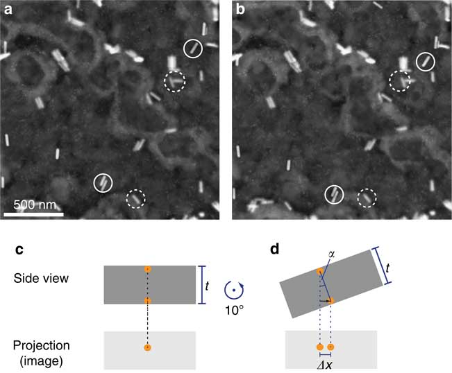
Figure 2 Determination of the total thickness t of the aluminum film and silicon nitride membrane by means of tilting the specimen. a: ADF STEM image showing Au nanorods at a specimen tilt angle α=0°. Exemplary Au nanorods on top of the Al film (in focus) and at the bottom (imaged out of focus) are encircled by full and dashed circles, respectively. b: Image of the same region tilted by an angle α=10° in x direction. c: Schematic drawing of the projection of in image acquisition. At α=0°, two particles at the top and the bottom of the aluminum film superimpose each other in the projection of the electron micrograph. d: If the sample is tilted, these particles will appear displaced in the projection by Δx.
The thickness was determined by acquiring images at four to five different positions for each sample for non-tilted and tilted orientations (Table 1). It followed that the samples were not flat within nanometer range but thickness variations occurred. The average thickness of samples 1–3 with four Al layers amounted to t=0.60±0.05 µm, which was considered as the thickness measure for these samples. For sample 4, t=0.98±0.06 µm. A further complication was that brightness variations in overview images (e.g., in Fig. 2) implied that the Al film was not deposited entirely homogenously; some areas of the background appear brighter, other darker. The density of the evaporated Al thus cannot be assumed to be equal to the density of bulk Al.
Table 1 Sample thicknesses (including silicon nitride of 0.05 µm thickness and Al layer) of the four microchips used for this study measured at different lateral positions at the sample.
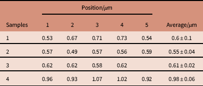
The error margin reflects the standard deviation.
Second, the vertical locations of the AuNP layers were determined (Table 2). AuNPs in sample 1 were located above one layer of Al and underneath three layers at z=0.18±0.03 µm, relative to the bottom SiN window. The thickness of the Al layer (minus SiN layer) was thus 0.13±0.03 µm. The AuNPs in sample 2 were at the second Al layer, and in 3 above three layers of Al. For sample 4, the AuNPs were located at the second Al layer.
Table 2 Vertical positions z of the AuNPs in the different samples determined by the tilting experiments.
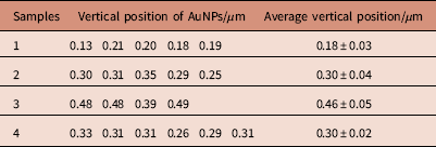
The position measures the layer depth with respect to the bottom of the silicon nitride membrane.
Measuring the Spatial Resolution for AuNPs at Different Vertical Locations
The thickness of the aluminum film above the AuNPs showed a significant effect on the achieved spatial resolution in the image. Two electron micrographs of identical particles but imaged from different sides of the SiN membrane (by flipping the specimen) are exemplarily displayed in Figures 3a and 3b, for sample 3. The AuNPs shown in Figure 3a were located below 0.15±0.05 µm of Al, whereas they were below 0.46±0.05 µm of Al and SiN in Figure 3b. The focus of the electron microscope was adjusted such that the AuNP layer was in focus. The AuNPs in Figure 3a appear sharper and smaller ones are visible than in Figure 3b. The apparent blurring effect was due to probe broadening and not to geometric broadening because the same vertical layer was imaged in-focus for both images. Samples 2 and 3 were imaged from both sides to obtain 5 different vertical positions together with the measurements of sample 1. In sample 4, the 1.0 µm-thick Al film, the AuNPs could only be imaged in the flipped orientation with the AuNPs positioned below a 0.30±0.03 µm thick layer of Al and SiN. When the sample was inverted so that the AuNPs were embedded at a vertical depth of 0.7 µm, they were not visible. This indicates that the beam broadening had become so strong that the electron probe became significantly larger than the AuNP diameter and that the contrast became too low.
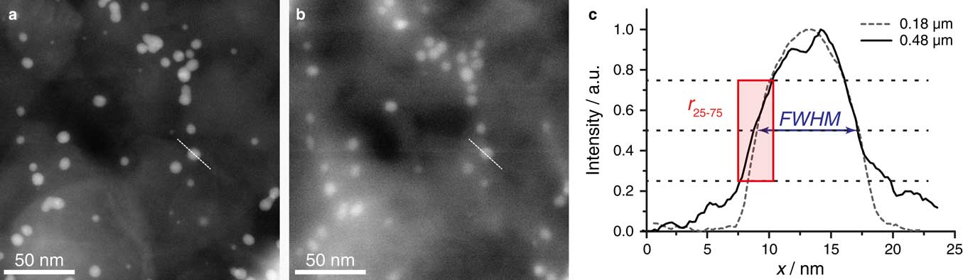
Figure 3 STEM micrographs of AuNPs in the same sample area but imaged from opposite sides with respect to the SiN window of sample 3 of a total thickness (Al and SiN) of 0.61 µm. a: Image of AuNPs underneath a 0.15-µm thick layer consisting of Al. The focus of the STEM probe was adjusted to the vertical position of the 5- and 10-nm diameter gold nanoparticles. The pixel size was 0.24 nm and the electron dose amounted to 3,700 e-/Å2. b: Image with the sample positioned upside down with respect to the schematic shown in Figure 1. so that the AuNPs were underneath 0.46 µm of Al and SiN. The focus of the STEM probe was again adjusted to the vertical position of the gold nanoparticles. c: Line profiles along the dashed lines in (a) and (b). The line profile was smoothed. Two resolution measures are indicted, the full width at half maximum FWHM, and the 25–75% rising edge width r 25–75.
In total, 143 intensity profiles over AuNPs at different vertical depths were analyzed in all four samples. Where possible, we compared intensity profiles of identical particles imaged from both sides. An example is shown in Figure 3c. The intensity profiles were taken over the particle indicated by the dashed lines in Figures 3a and b and normalized to 1. In general, profiles of particles located closer to the top surface appeared smoother, that is less noisy, than those of particles at higher vertical depth, reflecting a larger SNR. The curves overlapped well at normalized intensities above 0.5, almost independently of the vertical depth of the particles. The slopes of the peaks at lower intensities, however, significantly flattened for AuNPs under thicker layers of aluminum, reflecting the appearance of so-called beam tails (Demers, et al., Reference Demers, Ramachandra, Drouin and de Jonge2012).
In order to quantify the observations of the beam blurring effect, the full width at half maximum FWHM, and the r 25–75 (Reimer & Kohl, Reference Reimer and Kohl2008) were determined from all 143 intensity profiles in the same manner as illustrated in Figure 3c. The FWHM and r 25–75 were compared for all 143 intensity profiles (Fig. 4a). Remarkably, the FWHM appears to be independent of the vertical position of the AuNPs, and hence of the broadening of the electron beam. The FWHM of particles imaged under a thickness of 0.15 and 0.46 µm, respectively, differed only by 10%. In contrast, the r 25–75 value increased by a factor of 2.5 on average with increasing vertical depths of the AuNPs. Thus, the FWHM and r 25–75 resolution measures did not correlate.
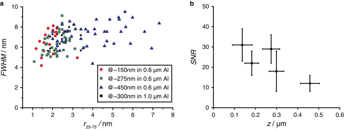
Figure 4 Measurement of the spatial resolution using either the FWHM or the r 25–75 for AuNPs at different vertical positions and for different sample thicknesses. a: Relation of the FWHM to the r 25–75 for AuNPs located at different vertical locations. b: Signal-to-noise ratio (SNR) obtained on imaging AuNPs at different vertical positions z for a sample thickness of 0.6 µm.
The measure of r 25–75 is not ideal but it is the best measure when the STEM probe is smaller than the round nanoparticles, whereas the FWHM becomes a better measure once the probe diameter becomes larger than the nanoparticles (Ramachandra et al., Reference Ramachandra, Demers and de Jonge2013). In our case, the nanoparticles were apparently larger than the probe size, and so the FWHM measured the same values for the nanoparticles imaged and is thus not a useful measure.
We also determined the SNR as function of z for the samples of 0.6 µm thickness (Fig. 4b), whereby the signal and the background reflect the pixel intensity values obtained at an AuNP and the background in its vicinity, respectively. The standard deviation of the background is a measure of the signal fluctuations. Figure 4b shows that the SNR decreased with increasing z even though the sample thickness was constant. This can be understood by considering that the focused electron probe contains fewer electrons, due to larger beam tails, the deeper it propagates into the sample. The SNR is higher than what would be required on the basis of the Rose criterion (Rose, Reference Rose1948).
The r 25–75 values are plotted as function of z in Figure 5. Probe broadening is not limiting the spatial resolution up to a depth of 0.27 µm but the broadening increases rapidly for AuNPs positioned at larger depths. There is no significant difference between the sample of t=0.6 and 1.0 µm. For AuNPs at the top of the sample 1 of t=0.6 µm a value r 25–75=1.5±0.5 nm was measured. Here, the electron probe was unperturbed and of negligible width so that the r 25–75 is a measure of the size of the AuNPs.
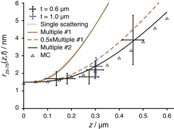
Figure 5 Dependency of the r 25–75 on the vertical position z of the AuNPs in a sample for thicknesses t=0.6 and 1.0 µm of the Al matrix including SiN. The error margins reflect standard deviations. The following theoretical curves are included: (1) numerical calculation based on the model of a single scattering event (Goldstein, Reference Goldstein1979), (2) multiple scattering model 1 (Reimer & Kohl, Reference Reimer and Kohl2008), (3) corrected multiple scattering model 1 multiplied by 0.5, and (4) modified multiple scattering model 2 (Gauvin & Rudinsky, Reference Gauvin and Rudinsky2016). Monte Carlo simulations are also included for a samples of t=0.6 µm and with AuNPs at different z, and all experimental conditions the same as in the experiment except that the electron dose was a factor of 100 larger.
Determining the Density of the Al Matrix
In order to determine the amount of electron scattering via calculation, we need to know the sample density, noting that the standard value for solid Al may not apply as sample inhomogeneities were observed (Fig. 2) in the evaporated Al. With the thickness of the samples t known from the tilting experiment, the effective density ρ Al,eff of the Al matrix was calculated from measurements of the scattered current. The current passing through the opening of the ADF detector was measured and used to determine t via equation (9) using the detector opening inner semi-angle of 43 mrad. The sample was considered to consist entirely of Al, which is valid as approximation, as l Al=1.0 µm and l SiN=0.8 µm for this opening angle, and the thickness of the SiN membrane is only 0.05 µm. To calculate l SiN, we used Z=10.6, W=20 and ρ=3.2×10⁶/gm3 (de Jonge et al., 2010 Reference de Jonge, Bigelow and Veitha ). For sample 1 with t=0.64 µm, a fraction of transmitted current of 0.52 was measured; the fraction of current scattered by angle of 43 mrad or larger is thus 0.48. Solving equation (9) resulted in ρ Al,eff=2.6×10⁶/gm3, slightly smaller than the density for solid Al of 2.70×10⁶/gm3. But considering the error margin of the measurements, the density of solid Al can be assumed on average.
Comparison with Monte Carlo Simulation
An important question is whether the data reflects the intended measured parameters. In particular, it needs verification that an increasing r 25–75 actually measures increased beam broadening for AuNPs located at increasing vertical depth, and not some other effect. For example, the STEM imaging was performed with a conical beam, whereas the beam broadening models typically assume a pencil beam shape. Although the focus was always adjusted to the vertical position of the imaged AuNPs and geometric broadening was thus absent, additional beam broadening could possibly have played a role. The electron probe has a double cone shape (Fig. 1) and electron scattering occurs throughout the entire cone. When the focus is adjusted to particles deeper within the sample, the size of the electron probe is enlarged by 2αz at the vertical location where it enters the sample, which is the maximum diameter from which electron scattering occurs. All scattered electron trajectories contribute to the beam blurring.
Monte Carlo simulations were performed to examine the measured data. The same sample geometry and microscope settings as used for the experiments were used for the Monte Carlo simulation of lateral line scans. A line scan of a scanning STEM probe of an AuNP was simulated at a certain vertical depth in the sample for the same electron dose as used for the experiments (Fig. 6). Two beam convergence semi angle α were simulated: 0.0 and 20 mrad. The overall signal for the larger α was higher but the peak over the AuNP had the same width. Additional line scans were simulated for AuNPs at different vertical positions ranging from 0 to 600 nm. As the signal obtained on AuNPs at deeper layers than 0.3 µm decreased in SNR, the electron dose was increased by a factor of 100 so that it was possible for precisely determine the r 25–75 values for α=20 mrad (see Fig. 5). The same data points were also simulated for α=0.0 mrad (data points overlap in Fig. 5 and are not indicated separately) but significant differences in r 25–75 were not visible and so the beam convergence angle does not influence beam blurring at this parameter range.
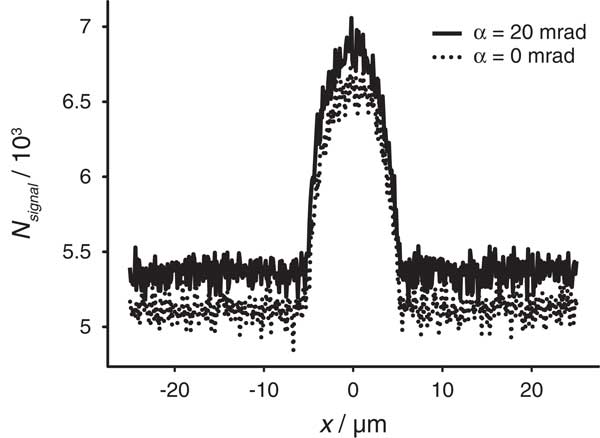
Figure 6 Monte Carlo simulation of scattered electrons collected in the ADF detector N signal as function of the horizontal position x of a focused electron probe. Line scans were calculated for two values of α 21,346 electron trajectories were used, which corresponds to a dose for an electron probe current of 180 pA and a pixel dwell time of 19 µs. The sample was 600 µm thick and the AuNP layer was 0.1 µm below the top surface. A 50-nm thick AiN layer was at the bottom.
A further question is whether angular changes by inelastic scattering need to be taken into account. Monte Carlo simulation again gives an answer. In the Casino software, each electron trajectory is simulated by computing the elastic scattering events only. The Monte Carlo simulations do not take angular changes due to inelastic scattering into account. Yet, the inelastic events are approximated by the mean energy loss between two elastic scattering events only. The mean energy loss rate is given by the modified Bethe equation (Joy & Luo, 1989) with relativistic correction. However, as the Monte Carlo simulation accurately describes the data, it can be concluded that angular changes by inelastic scattering does not need to be accounted for when examining beam broadening.
Comparison of Experimental Data with Theoretical Models
The measured spatial resolution was compared with the predictions of theoretical models (Fig. 5) to examine the influence of beam broadening. The theoretical model calculated the r 25–75 as follows:
 $$r_{{25{\minus}75}} \,{\equals}\,\sqrt {r^{2} _{{25{\minus}75}} ,\,{\rm AuNP}{\plus}r^{2} _{{25{\minus}75}} ,_{{{\rm blur}}} } .$$
The value of r 25–75, AuNP=1.5 nm from the measurements at z=0 was used.
The SNR-limited resolution was found to be negligible based on the following calculation. For the ADF detector angle β=68 mrad, equation (11) gives d SNR=0.91 and 1.4 nm for t=0.6 and 1 µm, respectively. Thus, much smaller AuNPs than actually imaged can be detected with the used microscopy settings, which is consistent with the measured high SNR values (Fig. 4b). Much smaller r 25–75 values would have been observed had the recordings been made with AuNPs of diameters<1.4 nm. For example, an AuNP of a diameter of 1.0 nm in the top layer of the sample imaged with an electron probe of d 50=0.2 nm (diameter containing 50% of the current), would have resulted in a measured r 25–75=0.35 nm for sampling at twice the corresponding spatial frequency. This finding also implies that the measured data does not depend on t within the range of the experiment.
As a first comparison with theory, the model of a single scattering event in the middle of the sample (Goldstein, Reference Goldstein1979) was evaluated. But instead of using the published equation (13), approximating the probe diameter to contain 90% of the current, equation (9) was solved numerically to obtain the angle β max of the cone containing 90% of the current for different values of z. The aim was to avoid the approximations needed to derive equation (13). A Gaussian beam profile was assumed. From computing this beam profile, it followed that d 90/r 25–75=3.6, and this factor was used to compare the calculated d blur with the experimental data. Figure 5 shows that this model overestimates the measured beam blurring in particular for larger z where multiple scattering more likely occurs. Although the slope z 1.5 in the model seems to be correct (see below), the absolute values are incorrect for determining the STEM resolution for AuNPs at deeper layers in the sample. Testing this model for d 50 and d 25 (de Jonge et al., 2010 Reference de Jonge, Poirier-Demers, Demers, Peckys and Drouinb ) did not lead to an improvement of the accuracy (calculated data not shown). The model in which beam blurring is calculated from a single scattering event is thus incorrect.
Second, equation (14) was compared with the data. This equation is an estimate that includes also multiple scattering (Reimer & Kohl, Reference Reimer and Kohl2008). Here, d blur already reflects the r 25–75, so that a conversion is not needed. Figure 5 shows that this model overlaps with the single scattering model resulting in a similar slope of z 1.5 but with much too large a value of d blur. As it was stated previously that the model overestimates the beam blurring by a factor of two (Reimer & Kohl, Reference Reimer and Kohl2008), we also computed d blur/2, and indeed a better match between data and model was obtained. The model just misses the data point at z=0.27 µm but matches the data within the error bars for the other data points. This is also consistent with previous data, showing that d blur approximately matched experimental data (de Jonge et al., 2010 Reference de Jonge, Poirier-Demers, Demers, Peckys and Drouinb ) and Monte Carlo simulations (Demers et al., Reference Demers, Ramachandra, Drouin and de Jonge2012) using the FWHM as measure of beam broadening and noting that d FWHM /r 25–75=2.6, accounting for the factor of two difference.
The model of equation (14) can thus be used to calculate beam blurring when it is corrected by a factor of two. However, this calculation with an extra factor lacks a scientific understanding of its origin, and it should thus be questioned if this model is generally valid.
Third, we tested a model that accounts for multiple scattering via a random walk approximation (Gauvin & Rudinsky, Reference Gauvin and Rudinsky2016) via equation (15). This equation is based on an estimate of the scattering angle θ*. Differing from the original paper, we calculated the most probable scattering angle of a single elastic scattering event from the expectation value <θ*> using the integral:
 $$\,\lt\,\theta ^{{\asterisk}} \,\gt\,{\equals}{{{\int}_0^\pi {\theta {{d\sigma } \over {d\Omega }}d\theta } } \mathord{\left/ {\vphantom {{{\int}_0^\pi {\theta {{d\sigma } \over {d\Omega }}d\theta } } {{\int}_0^\pi {{{d\sigma } \over {d\Omega }}d\theta } }}} \right. \kern-\nulldelimiterspace} {{\int}_0^\pi {{{d\sigma } \over {d\Omega }}d\theta } }}.$$
The value determined for Al amounted to <θ*>=11 mrad. Using equation (7), we then calculated the most probable path length between collisions l(<θ*>)=0.20 µm. The obtained values of <θ*> and l(<θ*>) were used in equation (15) to calculate the beam broadening. In addition, equation (15) was adapted to a measure in d 50. A one-dimensional random walk with variable path length results in an expected translation s after n steps of:
 $$\,\lt\,s\,\gt\,{\equals}\,0.67\sigma \sqrt n ,$$
when the path lengths exhibit a Gaussian distribution with normal distribution σ. The factor 0.67 scales s to 50% probability. Therefore, d blur in equation (15) was multiplied by 0.67 to obtain d 50. Division by 1.5 finally resulted in r 25–75. This model fits all data points within the margin of error (Fig. 5), and it also closely follows the trend of the Monte Carlo simulation.
Conclusions
The spatial resolution obtained with ADF STEM for imaging AuNPs embedded in a thin foil depends on the thickness of the foil and the vertical position of the objects, whereby two regimes are recognized. The resolution is independent of the vertical position for AuNPs close to the surface with respect to a downward traveling electron beam. But beyond a certain vertical location, beam broadening starts to dominate. The most precise way to calculate beam blurring is via Monte Carlo simulations, and this calculation accounts for multiple scattering. Inelastic scattering can be neglected when calculating beam broadening due to angular changes of the electron trajectories. Three theoretical models for beam broadening were tested. A traditional model, that considers beam broadening to occur via a single scattering event (Goldstein, Reference Goldstein1979), was tested via a numerical solution and found to be imprecise. A frequently cited model, including an estimate of multiple scattering (Reimer & Kohl, Reference Reimer and Kohl2008), overestimates beam blurring by more than a factor of two, but is approximately correct when this factor is included. A modification of a recent model describing multiple scattering via a random walk (Gauvin & Rudinsky, Reference Gauvin and Rudinsky2016) describes the data within the error margin of the experiment. For the later model, the most likely scattering angle <θ*> was calculated as key parameter, which can be readily adapted to other materials. The beam broadening depends on z 1.5 in all three models. These conclusions are presumably also valid for other materials and sample configurations.
Acknowledgments
The authors thank Michael Elbaum, Lothar Houben, and Raynald Gauvin for discussions, Anna Schreiber for the deposition of aluminum films by means of physical vapor deposition and E. Arzt for his support through INM, Research supported by the Leibniz Competition 2014.


