


Introduction
One of the most time-consuming tasks in materials characterization labs is the preparation of high-quality samples for high-resolution S/TEM (transmission and/or scanning transmission electron microscopes, collectively) analysis. The samples must be thin—as thin as a few tens of nanometers—and thinner is almost always better for high-resolution images. Creating such samples without damaging the structures of interest is challenging, to say the least. Traditional methods can take several hours to many days to complete and, even in the most expert hands, may still deliver samples of insufficient quality.
Focused ion beam (FIB) and DualBeam FIB/SEM (scanning electron microscope) technologies have long been the methods of choice to create site-specific samples that must contain a specific structure from a known location within the bulk sample [Reference Giannuzzi1]. Recent advances in microscope technology, especially in the area of automation, have dramatically increased the speed, ease, and reliability of the preparation process, ensuring fast, high-quality results [Reference Van Leer and Wall2,Reference Wall3]. This is even the case for less experienced operators, making the technique a viable alternative to conventional methods even when site specificity is not required. In this article, we will review the requirements for high-quality samples in S/TEM analysis, outline the benefits of using FIB/SEM technology for S/TEM sample preparation, present a novel approach to S/TEM sample preparation based on a guided workflow, and demonstrate the workflow as part of a use case.
Materials and Methods
Thin specimen requirements
High-resolution scanning/transmission electron microscopy (HR-S/TEM) is an excellent method for studying the structure of materials at the atomic level [Reference Langford and Petford-Long4]. Modern TEMs can correct for the spherical aberrations inherent in the magnetic lenses used to focus electrons, provide direct visualization of the atomic order of crystals, and determine the position of individual atoms to within a few tens of picometers. Obtaining the best results in HR-S/TEM requires near-perfect samples [Reference Schaffer5]. In addition to acquiring high-quality data from a single sample, the scientific method requires that the results also be reproducible, meaning that other samples extracted from a bulk material by the same operator or another operator should deliver the same results with regards to structure, morphology, and elemental composition. In order to achieve these high-quality, reproducible results, the samples must exhibit certain characteristics:
-
∙ Thinness: The sample must be thin enough for the beam to pass through to the detector, ideally with most electrons interacting no more than once with a sample atom.
-
∙ Surface quality: The surface of the samples should be flat and free from topographic artifacts or defects introduced by the milling process (for example, material sputtering). Amorphous surface damage from the thinning process must be minimized. This is important to ensure that the analysis of the sample is not compromised by changing the composition or structure of the initial material during the sample preparation process. The existence of amorphous surface damage will also degrade the contrast and resolution of TEM images.
-
∙ Thickness uniformity: The thickness of the created samples should be uniform so that analytical techniques that depend on the number of events occurring over the electron path length through the specimen, including many chemical and elemental analysis methods, can yield valid point-to-point comparisons of elemental distribution or particle/precipitate distribution across the sample.
-
∙ Parallelism: Closely related to thickness uniformity, the parallelism of the top and bottom surfaces plays a critical role in electron holography.
Semi-automated workflow
Recent advances in instrument design, particularly in the automation of both setup and operating routines, now permit the execution of a guided, semi-automated workflow for sample preparation that can rapidly and routinely prepare high-quality samples for high-resolution imaging techniques like S/TEM or atom probe microscopy [Reference Giannuzzi6]. Although the ability to automate certain portions of the preparation process has evolved steadily since FIB-based sample preparation was introduced, it has only now reached the point where essentially the entire process can be incorporated into a repeatable and easily executed guided routine. The workflow can be applied to a wide range of different materials, including silicon, steel, aluminum, ceramics, and soft materials. It is especially well-suited to multi-user facilities, even those serving operators with many levels of expertise. By automating segments of the process that do not require operator interaction and providing guidance for those segments that do require interaction, a well-designed workflow can: (a) help users of all experience levels routinely prepare site-specific, ultra-thin, high-quality in-situ lamellas for S/TEM analysis, (b) enable the user to achieve predictable results for a wide range of materials, typically in under an hour, (c) assist the user with low-energy polishing to improve the quality of final lamellas, and (d) dramatically increase TEM data acquisition, productivity, and quality.
Workflow design
The recipe for this semi-automated TEM sample preparation workflow was created using a visual scripting framework that enables automation of a wide range of instrument control commands and imaging tasks. The user can record customized sample preparation routines that can be saved as recipes for repetitive use. The integration of the automation software with a nanomanipulator (Thermo Scientific EasyLift) enables the user to easily and automatically lift the sample from the bulk material and smoothly transfer it to a TEM grid for further preparation. The design priorities for the workflow include:
-
∙ Minimizing user interaction: whenever possible the microscope automatically sets the system conditions required for each recipe step.
-
∙ Requesting user input only when interaction is required for a critical recipe step.
-
∙ Permitting the user to abort the recipe at any time.
-
∙ Attaching concise descriptions for each recipe step.
The workflow is essentially a sequence of three sub-processes: protection of the region of interest (ROI) and chunk milling; in-situ lift-out; and final thinning, including low-energy polishing (5 kV). Using the guided workflow, an operator can create samples that yield reliable and reproducible results and ultimately permit confident conclusions about the real structure, morphology, and composition of the material being analyzed in the TEM.
Results
AlGaN/GaN/AlN Multilayer Specimen
Al x Ga 1-x N has been studied extensively in the past several years because of this material’s ability to be used as an electron blocking layer in light-emitting diode heterostructures and as an active layer in potential ultraviolet-emitting optoelectronic devices [Reference Liu7]. There have been many attempts to produce both n-type and p-type conductivity thin films with mole fractions of x in the range of 0.35–0.6, but growth is challenging because of the high stress state of the films [Reference Einfeldt8].
In this example, interfacial stress within the mulilayer stack is examined by TEM for a given mole fraction to understand how growth conditions affect the thin films. The sample was prepared on a Thermo Scientific Helios G4 FX DualBeam FIB-SEM.
Step 1: Protection of ROI and chunk milling.
In a first step, the user interactively configures the lamella dimensions and milling conditions for the sample to be created. After locating the area of interest, the system automatically mills fiducial markers that will be used for accurate visual end-pointing during the final thinning stages of the workflow (note the patterned cross next to the lamella site in Figure 1. Next, the user selects the fiducial marker to determine the position of the deposition layer that protects the chunk sample during the milling process (Figure 1a). After the system automatically deposits the protective layer, the user selects the fiducial marker for bulk milling of the chunk at high beam current. The system automatically completes the bulk milling step and cleans up sputtered material redeposited on sample surface near the milling site (Figure 1b). The stage is tilted so the chunk can be separated from the bulk sample in the undercut step.

Figure 1 Protection of the region of interest and chunk milling. (a) Deposition layer that protects the chunk sample during the milling process. (b) Completed bulk milling step with bulk milling clean-up.
Step 2: In-situ lift-out
To ensure that the sample is at the eucentric position and coincident with the beam position, the user is prompted to select the fiducial marker with the SEM image and then the FIB image to align the stage for lift-out. This position will be used as a reference for the lift-out process and helps the user to safely operate the nanomanipulator. Next, the user selects the probe tip of the nanomanipular in the SEM image and aligns it in X and Y directions. The user is then prompted to select the probe tip in the FIB image to align the Z direction and lower the probe in two steps. The probe has thus been accurately positioned with respect to the sample with only three point-and-click movements. After accurately aligning the probe tip of the nanomanipulator, the user is prompted to confirm the position of the welding pattern that will attach the chunk to the probe tip, and the system executes the attachment procedure (Figure 2a). Prior to in-situ lift-out, small crosses are patterned onto the top of the TEM section to assist with final thinning of the section. Next, the user confirms the position of the right-side cut pattern to prepare the chunk to be released from the bulk. The system then cuts the chunk free from the bulk and extracts it to a safe position (Figure 2b).

Figure 2 Lift-out of the bulk chunk. (a) Attaching the nanomanipulator probe to the sample, and (b) lifting the “chunk” out of the bulk material. Figure 2b is an FIB image, and thus the rotation of the image is different.
Step 3: Grid attachment
The user is asked to move the stage to bring a 3-millimeter TEM grid into position, and the user selects the correct chunk attachment location on the grid in a series of prompts identifying the position with the SEM and FIB that ensures the grid is at the eucentric and beam coincident position. In order to attach the chunk sample to the TEM grid, the user selects the position of the welding pattern relative to the grid and the sample, and the system executes the grid attachment procedure (Figure 3a). In the final steps, the user confirms the position of the cut pattern to separate the needle from the sample, the system cuts the nanomanipulator free, and the user verifies that the probe is free from the lamella and retracts the nanomanipulator (Figure 3b).

Figure 3 Grid attachment. (a) TEM grid is moved into position near the sample. (b) Sample attached to the TEM grid.
Step 4: Final thinning
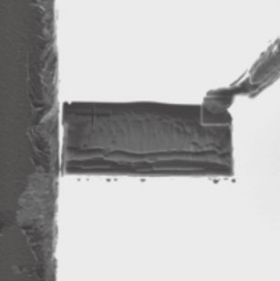
Before starting the final thinning process, the user is prompted to confirm the eucentric and beam coincident position of the sample in the microscope by identifying the free edge of the section in the SEM and FIB, respectively. The system can accurately place the FIB milling patterns with the recipe once the positions of the markers are identified by the user (the small cross patterns in Figures 2a and 3a). In a first thinning step, the system mills the front and backside of the lamella with a 30 kV, ~2 nA beam at a small “pre-tilt” angle to the surface. In subsequent steps, the system repeats the milling process using progressively lower currents after the user identifies the cross-patterns on top of the section. The system automatically thins the sample to the desired thickness (Figure 4a), ending with a final polish at 5 kV to remove surface damage and the amorphous layer (Figure 4b). If required, further thinning with FIB energies down to 500 V may be employed to further reduce surface damage and ensure the sample is thin enough for the required TEM analysis.

Figure 4 Final thinning and polishing. (a) Sample during thinning process. (b) Finished sample after low-energy polishing at 5 keV.
Imaging and analysis
The AlGaN/GaN/AlN multilayer sample, prepared using the semi-automated workflow, was then imaged in an Thermo Scientific Themis probe-corrected STEM equipped with a SuperX detector consisting of four windowless silicon drift detectors (SDDs). Figure 5 shows STEM images of the specimen taken with a HAADF detector. Figure 5a shows an overview of the sample. The sample has a uniform thickness of about 0.4 of the mean free path in this material. Figure 5b shows AlGaN/GaN layers at atomic-level resolution. These images illustrate the success of the semi-automated workflow in FIB-based sample preparation. Figure 6 shows element maps from an EDS spectrum image collected using 200 pA beam current for 10 min. The EDS maps show the separations of the AlGaN/GaN/AlN layers. Lastly, Figure 7 shows the spectra from two areas of the EDS maps. Raw data illustrate the spectra from the GaN and AlN regions. There was no indication of Ga in the AlN region, indicating that final polishing with 500 V Ga+ FIB can be an excellent method for preparing high-quality Ga-containing samples.

Figure 5 High-angle annular dark-field (HAADF) STEM images of AlGaN/GaN/AlN multilayer collected at 300 keV using a Themis probe-corrected TEM. (a) is a survey image of the device, and (b) shows atomic columns containing Ga atoms.

Figure 6 X-ray element maps of specimen area in Figure 5a collected at 300 keV using a SuperX detector on a Themis probe-corrected TEM. The image at the left is a STEM HAADF image followed by the Ga map, Al map, N map, and a composite map of Ga and Al maps. From these maps the features in the STEM image can be determined: bright regions are GaN, gray regions are GaAlN, and dark regions are AlN.

Figure 7 HAADF STEM and spectra at 300 keV from two areas of the X-ray spectrum image. Raw spectral data from the GaN area (red) and the AlN area (blue box) indicate the identity of these phases.
Bismuth-doped lead zirconate titanate
Ferroelectric lead zirconate titanate (PZT) thin films have been intensively studied in recent years as candidates for use in ultra-large-scale-integration (ULSI) dynamic random access memories (DRAM), nonvolatile random access memories (NVRAMs or FRAMs), pyroelectric sensors, and electro-optical applications [Reference Klingon and Srinivasan9]. A variety of PZT-based materials compatible with these applications has been developed via various compositional modifications and changes in the methods of chemical synthesis and processing. It is well established that doping with cations, such as La, in PZT thin films and PZT ceramics causes their dielectric and ferroelectric properties to change.
In this example, bismuth is examined as a new dopant for PZT thin films in the hope that a large, reversible, and spontaneous polarization exhibited by the doped material makes it an attractive candidate for FRAM applications. In the present analysis, it was of interest to study the nanostructure formed inside the domains of these ceramics, as well as the structure of the domain boundaries.
Workflow
The guided workflow here followed the same steps as above: the user/system selects the area of interest, deposits a protective layer of platinum, mills two large trenches on either side of the region of interest, and cleans up the surfaces of the cross section while applying slight tilt to maintain parallel side walls (Figure 8). The sample is then attached to the nanomanipulator, lifted out of the bulk sample, and attached to a TEM sample grid. Final cleaning of the cross section was applied to both sides of the lamella using a 30 kV ion beam energy and tilting the sample into the beam. To complete the sample, a low-energy cleaning step was applied to both sides of the lamella to remove any residual amorphous material (Figure 9).

Figure 8 Initial steps. (a) Protective deposition layer over the region of interest. (b) Bulk milling completed after final bulk milling clean-up.

Figure 9 Final steps. (a) Sample during thinning process. (b) Sample after final low-thinning process. Note that the thinned area becomes progressively thinner and smaller toward the center of the section.
Imaging and analysis
After the semi-automated workflow was used to prepare the sample in the SEM/FIB system (Thermo Scientific Helios DualBeam), the operator transfered the sample to the electron microscope (Thermo Scientific Talos F200X S/TEM) for high-resolution TEM and STEM-EDS spectrum imaging analysis. The high-resolution TEM image in Figure 10a was acquired using a 4k × 4k Thermo Scientific Ceta camera and shows the PZT crystal. Figure 10b shows the digital magnification of a region of Figure 10a, which reveals the crystalline structure of PZT. The corresponding Fourier transform of the image (Figure 10c) contains spatial frequencies corresponding to 0.12 nm, which is the specified information limit of the Talos F200X S/TEM. Figure 11 shows the spectra from two areas of the X-ray spectrum image. The raw X-ray spectral data indicate the presence of two phases; one containing Ti, Pb, Nb, Zr, Al, and Mg (area 1) and one rich in Si, Mg, and O (area 2). The elements in these phases are also shown in the X-ray maps of Figure 12. Compositional information could be obtained with the SuperX detector despite the small acquisition time of only 3 minutes. These figures show that the sample prepared using the semi-automated workflow is suitable for TEM and STEM characterization.

Figure 10 High-resolution imaging of PZT. (a) TEM image acquired using a 4k × 4k camera. (b) Digitally magnified region from the white box in (a) showing atomic columns. (c) Fourier transform of the full 4k × 4k TEM image with a circle indicating the information limit of 0.12 nm.
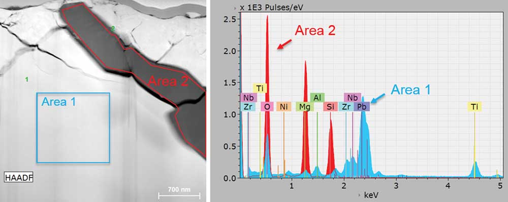
Figure 11 STEM image of PZT phases acquired using a Talos F200X S/TEM at 200 keV. (left) Image recorded in parallel with the STEM X-ray spectrum image. (right) X-ray spectra of the two phases within the field of view.

Figure 12 Elemental maps showing two phases in PZT from the same sample region as Figure 11. These X-ray maps were retrieved from a spectrum image collected at 200 keV using a SuperX detector on a Talos F200X S/TEM.
Conclusion
The characterization of materials via high-resolution STEM (HR-STEM) requires sample preparation meeting a range of distinct criteria: the preparation must repeatably deliver high-quality thin sections that precisely capture the region of interest. A guided, automated workflow has been described that permits various users, with a range of experience and expertise, to produce thin samples in about an hour that meet the requirements for repeatable high-resolution S/TEM analysis. The net result is a significant broadening of access to high-quality S/TEM analysis for researchers across many disciplines. This workflow encourages an increase in laboratory productivity with concomitant reductions in per-sample cost.
Acknowledgements
The authors would like to thank Tom Nuhfer of Carnegie Mellon University for providing the AlGaN/GaN/AlN multilayer LED specimen and the Laboratory for Equipment and Materials Testing (LAPEM) for providing the bismuth doped PZT sample. Sample preparation and analysis was performed in the European and North American NanoPorts of Thermo Fisher Scientific.


