


Introduction
Wide bandgap GaN and its related materials have great potential for high power and high temperature microwave electronic device applications owing to their low intrinsic carrier concentration, high breakdown field, high saturation velocity, and excellent chemical stability [Reference Dmitriev, Irvine, Carter, Kuznetsov and Kalinina1-Reference Mohammad, Salvador and Morkoç3]. A significant amount of effort has been devoted to the development of various GaN-based field effect transistors (FETs) [Reference Binari, Kruppa, Dietrich, Kelner, Wickenden and Freitas4-Reference Zolper, Shul, Baca, Wilson, Pearton and Stall8], which has led to the demonstration of high performance GaN/AlGaN MODFETs [Reference Chen, Keller, Parish, Vetury, Kozodoy, Hu, Denbaars, Mishra and Wu9-Reference Eastman, Chu, Schaff, Murphy, Weimann and Eustis12]. Compared to MESFETs and MODFETs, JFETs provide a higher gate voltage swing and a lower reverse gate leakage current due to a higher built-in potential of the p-n junction gate than the Schottky gate used in MESFETs and MODFETs. This is especially important for high temperature operation. In addition, the junction gate is metallurgically more stable and environmentally more robust than a Schottky gate since it is effectively buried beneath the surface and is subjected to high temperature during crystal growth. Therefore, JFETs are expected to withstand higher temperature operation than MESFETs and MODFETs. In this paper, we report the fabrication and characterization of epitaxially grown GaN JFETs.
Material and Fabrication
The epitaxial structure of GaN JFETs was grown by metal organic chemical vapor deposition (MOCVD) on a C-plane sapphire substrate. The layer structure consisted of a 4.2 µm semi-insulating GaN buffer layer, a 950 Å Si-doped n-GaN channel, a 60Å undoped GaN, and a 500 Å Mg-doped p-GaN. The sample was annealed at 850 °C for 15 sec in N2 to activate the Mg dopant. Hall measurements showed a free carrier concentration of 1.3×10¹⁸, 2.4×10¹⁸, and 6.1×1014 cm−3 in the p-GaN, n-GaN, and SI-GaN, respectively. The electron mobility in the n-GaN active layer was 270 cm2/V-sec. The fabrication process began with a mesa isolation etch in an inductively coupled BCl3/Cl2/Ar plasma. Next, a gate metal of Ni/Au/Ni was e-beam evaporated on top of the mesa and used as the mask for the self-aligned source-drain etch in a BCl3/Cl2/Ar ICP discharge. The device was completed with Ti/Al source and drain ohmic contact metallization. Post-metallization annealing was not performed. A transmission line method (TLM) measurement showed an as-deposited source and drain ohmic contact resistance of 4.2 Ω-mm, a specific contact resistance of 5×10⁻⁵ Ω-cm2, and a sheet resistance of 4700 Ω/square, respectively. These values were relatively large, possibly due to plasma induced damage and an overetched source and drain region.
Results and Discussion
Table I summarizes the DC and microwave result of a 0.8 μm × 50 μm GaN JFET with a source-drain spacing of 3 μm. A maximum ID of 270 mA/mm and a maximum gm of 48 mS/mm were measured at VG =1 V. A RS of 8.5 Ω-mm and a RD of 13 Ω-mm were obtained using the end resistance measurement technique. From the above result, an intrinsic transconductance (gm0 ) of 81 mS/mm was calculated. The channel was completely pinched off at a threshold voltage of VG =-8 V, with an ID =210 μA/mm at VD =15 V. A gate-drain diode reverse breakdown voltage of 56 V was achieved, which corresponded to a breakdown field of 2.5×10⁶ V/cm. The fact that the breakdown field approached the theoretical predicted breakdown field of GaN indicated that the relatively small breakdown voltage of the JFET as compared to the reported GaN MESFETs and MODFETs [Reference Binari, Kruppa, Dietrich, Kelner, Wickenden and Freitas4,Reference Eastman, Chu, Schaff, Murphy, Weimann and Eustis12] was primarily due to the high doping concentration in the n-GaN. The gate leakage current of our JFETs was large as compared to GaN MODFETs [Reference Binari, Redwing, Kelner and Kruppa13,Reference Wu, Keller, Keller, Kapolnek, Kozodoy, Denbarrs and Mishra14], possibly due to the plasma induced damage to the junction [Reference Osinski, Gangopadhyay, Lim, Anwar, Khan, Kuksenkov and Temkin15, Reference Van Hove, Hichman, Klaassen, Chow and Ruden16]. The forward turn-on voltage of the gate diode was ∼ 1 V using a 1 mA/mm current criterion. This value is only 30% of the bandgap energy of GaN. Pernot, et. al. have also reported a low turn-on voltage of 1.2 V on GaN p-n diodes [Reference Pernot, Hirano, Amano and Akasaki17]. The cause of this low turn-on is not known at present but may result from defect levels in the GaN.
Table I: DC and microwave characteristics of a 0.8 µm × 50 µm GaN JFET.

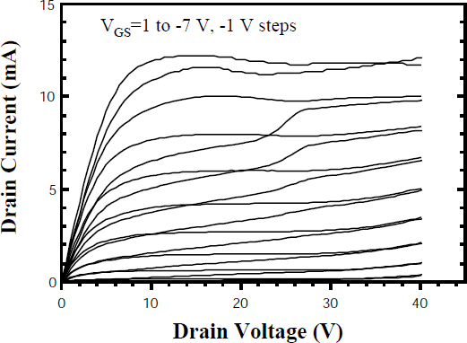
Figure 1: ID-VD characteristic showing the drain current collapse at VD< 25 V due to a partially depleted channel by electrons trapped in the SI-GaN. The solid curves were measured individually with 5 min of illumination to release trapped electrons in the SIGaN. The dashed ones were measured in rapid recession.
Similar to what Binari and co-workers have reported on GaN MESFETs [Reference Binari, Kruppa, Dietrich, Kelner, Wickenden and Freitas4], a significant reduction in ID occurred in our JFETs after they were subjected to a high VD . Figure 1 shows two sets of ID -VD curves measured up to VD =40V under white-light illumination. The solid curves were measured individually with 5 minutes of illumination before each curve was taken while the dashed curves were measured in rapid succession. The upper dashed trace (VG =1 V) is nearly identical to the upper solid trace since they were both subjected to a long illumination. The subsequent dashed curves exhibited a large decrease in ID at VD <25 V. This current collapse effect was not obvious unless VD was increased above 20V. The reduction in ID was caused by high-field injection and subsequent trapping of electrons in the SI-GaN, which depleted part of the active channel from the backside. We have demonstrated that these trapped electrons were located at the drain side of the channel where the electrical field was the highest [Reference Zhang, Lester, Baca, Shul, Chang, Willison, Mishra, Denbaars and Zolper18]. At VD <5 V, the transistor was below saturation and the current was limited by RS , RD , and the channel resistance, RCH . Since the channel was partially depleted by the trapped electrons, a lower channel conductance was obtained for the dashed ID -VD curves as compared to the solid ones in Figure 1. Above the knee voltage, it was assumed that the channel consisted of a velocity-saturated section in parallel with a space-charge region caused by trapped electrons in the GaN buffer. The latter was evidenced by the nearly constant output conductance between the knee voltage and VD =25 V. The rapid increase in ID of the collapsed curves at VD ∼25V may indicate a local breakdown of the space charge region. Therefore, regardless of illumination, ID at VD >25V was limited by an undepleted, velocity-saturated region on the drain side of the space charge layer.
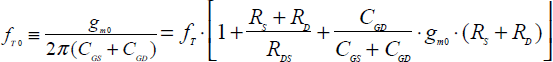
The microwave performance of the JFETs was characterized using an HP 8510 network analyzer. A unity current-gain cutoff frequency (fT ) of 6 GHz and a maximum frequency (fmax ) of 12 GHz were obtained at VD =15 V and VG =0 V from the small-signal S-parameters. These values were comparable to the reported fT and fmax on GaN MESFETs and GaN/AlGaN MODFETs with a similar gate length [Reference Aktas, Fan, Botchkarev, Mohammad, Roth, Jenkins, Morkoç and Kehias19, Reference Wu, Keller, Keller, Kapolnek, Denbarrs and Mishra20]. The intrinsic fT of our JFETs would be higher by taking into account the large source and drain resistance. Following the derivation made by Tasker and Hughes [Reference Tasker and Hughes21], we were able to calculate fT0 of the JFETs by de-embedding the effect of the parasitic RS and RD from measured fT . From [Reference Tasker and Hughes21], the extrinsic cut-off frequency

where CGS , CGD , and RDS are the gate-source, gate-drain capacitance, and output resistance, respectively. Rearranging this equation, the intrinsic cut-off frequency
where
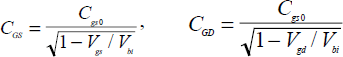
respectively. Cgs0 is the zero-bias gate-source capacitance, whereas Vgd =VG-IDRS and Vgd =VG-(VD-IDRD) are the voltage-drop across the p-n junction on either side of the channel, respectively. From the above equations, we obtain
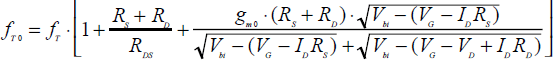
Since all the variables on the right hand side are directly measurable, this equation provides a simple method to extract the intrinsic fT0 from parasitic-limited FETs. An fT0 of 10 GHz was calculated for GaN JFETs using DC measurement results.
In order to estimate the ultimate speed that can be achieved in our JFETs, a calculation was made to simulate the change in gm as Lg decreases. Figure 2 shows the calculated gm vs. Lg curves for various saturation velocity (vs ). A 60% increase was obtained in gm as the Lg reduced from 0.8 to 0.1 µm. By fitting the gm of the GaN JFETs into this plot, a vs of 6.6×106 cm/s was obtained. Notice that the gate capacitance decreases linearly as the gate length shrinks. In addition, the electron velocity can exceed the vs in ultra-short gate length FETs due to velocity overshoot under high electrical field. Considering all these effects, an fT in excess of 50 GHz could be expected in GaN JFETs upon further improving the device design and process techniques, and scaling down the gate length. Also shown in Figure 2 were the reported gm values of GaN MODFETs and MESFETs. The data are somewhat scattered, possibly due to different material quality for different research groups. The gm of GaN JFET is comparable to most of them, suggesting a reasonably good quality
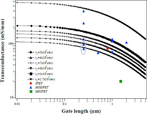
Figure 2: Simulation result of gm as a function of Lg for various vs values. The transconductance of GaN JFETs and reported GaN MODFETs and MESFETs are also shown for comparison. of JFET material.
In the above analysis, the effect of non-ideal ohmic contact to p-GaN on the gm and fT has not been considered. For microwave operation, the large gate displacement current causes a significant voltage drop on the gate resistor, leading to a reduced gm and fT . In addition, the extra capacitance at metal-p-GaN interface caused by the Schottky-type Ni/Au to p-GaN contact results in a further reduction in the fT . In order to optimize the performance of GaN JFETs, a low resistance metal contact to p-GaN with ideal ohmic I-V characteristic needs to be developed.
The DC performance of the GaN JFETs was also studied at elevated temperatures. The measurement was made on a hot plate in atmosphere. Figure 3 shows the plots of ID and gm as a function of VG at different temperatures. A continuous deterioration in ID and gm was observed with increasing temperatures up to 200°C where the device failed after being heated in the air for ∼2 hours. As the temperature was increased from 25°C to 200°C, ID dropped from 270 mA/mm to 75 mA/mm and gm was reduced from 48 mS/mm to 12 mS/mm, respectively. This was mainly caused by the reduction in electron mobility at elevated temperatures due to enhanced polar optical phonon scattering. However, the ID -VD curve exhibited an excellent pinchoff at a gate bias of –8 V, indicating a negligible gate leakage current. The failure of the JFETs after high temperature measurement was caused by the degradation of Ti/Al ohmic contact. An inspection of the devices after measurement showed a broken metal connection at the sidewall of the isolation mesa. The mesa profile was highly anisotropic, which resulted in a poor coverage of Ti/Al metal over the sidewall. Hence, the oxidation of Al upon prolonged heating in the air caused an open circuit.
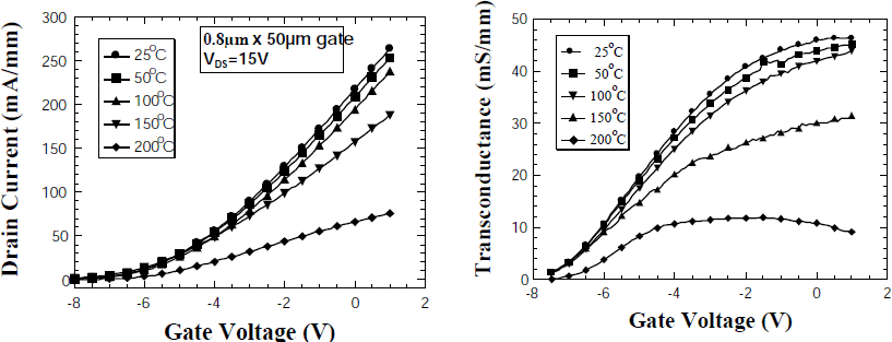
Figure 3: Drain current and transconductance as a function of gate voltage and measurement temperature.
Conclusion
In summary, JFETs were fabricated on an epitaxially grown GaN p-n junction. These devices exhibited excellent pinch-off and a breakdown voltage that agreed with theoretical predictions. An extrinsic transconductance of 48 mS/mm was achieved with a maximum ID of 270 mA/mm. Drain current collapse was observed in these devices after a high drain bias was applied due to partially depleted channel by the trapped electrons in the SI-GaN. The microwave measurement showed an fT of 6 GHz and an fmax of 12 GHz. A simple method was developed to extract fT0 from parasitic-limited FETs. An fT0 of 10 GHz was calculated for GaN JFETs using DC and rf results.
Acknowledgements
This work was supported in part by the National Science Foundation CAREER Grant ECS-9501785. Sandia is a multiprogram laboratory operated by Sandia Corporation, a Lockheed Martin Company, for the United States Department of Energy under contract DE-ACO4-94AL85000.


