Introduction
Silicon is the prefered n-type dopant in the growth of GaN. In hexagonal GaN (h-GaN) controllable Si-doping has been demonstrated for concentrations form 1017 cm−3 to 1019 cm−3 [Reference Doverspike and Pankove1]. At 300 K the luminescence intensity and the linewidth of the band-to-band transition increases monotonically with doping concentration [Reference Schubert, Goepfert, Grieshaber and Redwing2,Reference Iliopoulos, Doppalapudi, Ng, Moustakas and Symp3]. Photoreflectance measurements further showed for heavily doped h-GaN a shrinkage of the energy gap due to band-gap renormalization (BGR) effects [Reference Zhang, Chua, Liu and Chong4]. Detailed analysis of the electrical properties of Si-doped h-GaN further showed a significant influence of crystal defects [Reference Tang, Kim, Botchkarev, Popovici, Hamdani and Morkoc5] and of dislocations on the electron mobility [Reference Weimann, Eastman, Doppalapudi, Ng and Moustakas6, Reference Look and Sizelove7].
In this paper we summarize recent doping experiments of cubic GaN (c-GaN) epilayers by Si. Secondary ion mass spectroscopy (SIMS), photoluminescene (PL) at 300 K and 2 K and Hall-effect measurements are used to study the incorporation of Si, the optical and electrical properties of Si doped samples.
Experimental
The Si-doped cubic GaN epilayers are grown by an rf plasma assisted molecular beam epitaxy on semi-insulation GaAs (001) substrates at a substrate temperature of 720°C [Reference Schikora, Hankeln, As, Lischka, Litz, Waag, Buhrow and Henneberger8]. The growth rate is about 0.07 μm/h and the thicknesses of the layers are about 0.8 μm. Elemental Si is evaporated from a commercial effusions cell at source temperatures between 750°C and 1100°C, which correspondes to a variation of the Si-flux between 8.5*105 cm−2s−1 and 5.2*1011 cm−2s−1, respectively. The concentration and depth distribution of Si is measured by SIMS using Si implanted calibrated standards for quantification, and O2+ primary beam of 6 keV. Photo-luminescence measurements are performed at 300 K and in a He bath cryostat at 2 K. The luminescence was excited by a cw HeCd UV laser with a power of 3 mW and measured in a standard PL system. Hall-effect measurements were performed using square shaped samples at 300 K at a magnetic field of 0.3 T and with the samples in the dark. In was used for ohmic contacts.
Results and Discussion
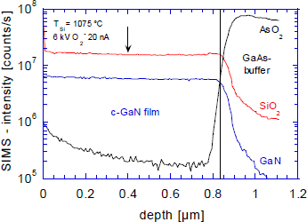
The incorporation of Si into c-GaN has been studied by SIMS. In Fig.1 the depth profiles of Si, GaN and As are depicted for a cubic GaN epilayer doped with elemental Si at a Si source temperature of TSi = 1075°C. A homogeneous Si distribution is measured throughout the whole c-GaN epilayer and no accumulation neither at the interface nor at the surface is observed. The Si-concentration measured at a depth of about 0.4 µ m (indicated by the arrow in Fig.1) is 2*1019 cm−3. In Fig. 2 the Si-concentration measured by SIMS (full squares) and the free electron concentration measured by Hall-effect at room temperature (full triangles) are plotted versus the Si source temperature. As clearly can be seen, both the free electron concentration and the amount of incorporated Si exactly follow the Si-vapor pressure curve (full line in Fig.2) at TSi > 1000°C [Reference Souchiere and Thien Binh9]. This indicates that nearly all Si atoms are incorporated at Ga sites and act as shallow donors. At room temperature the maximum free electron concentration reached so far is about 5*1019 cm−3. This clearly demonstrates the ability of controlled n-type doping of cubic GaN by Si up to concentrations which are necessary for the fabrications of laser diodes.

Figure 1. SIMS depth profiles of a Si doped
At room temperature the integrated intensity of the luminescence (full dots in Fig. 2) also follows the Si-vapor pressure curve, indicating that at 300 K the optical properties are also determined by the Si-doping and that even at the highest free carrier concentration of 5*1019 cm−3 no quenching of the luminescence is observed. The optical properties of Si doped cubic GaN at low temperature are shown in Fig.3. At 2 K the spectrum of the sample grown with the lowest Si-flux (8.5*105 cm−2s−1, TSi = 750°C) is dominated either by the excitonic transition X at 3.26 eV or by the donor-acceptor pair transition (D°, A°) at 3.15 eV [Reference As, Schmilgus, Wang, Schöttker, Schikora and Lischka10]. With increasing Si flux a clear shift to higher energies of the (D°, A°) is observed. In contrast to that, the transition X stays at its position as expected for an excitonic line. The peak position of the (D°, A°) as a function of the Si-concentration is plotted in Fig.4, where the Si concentration NSi was calculated by dividing the measured Si-fluxes by the measured growth rates. Using a simple Coulomb-term model [Reference Hopfield, Thomas and Gershenzon11] the peak position of the (D°, A°) transition can be estimated by


Figure 2. Si concentration measured by SIMS (full squares), free electron concentration measured by Hall-effect (full triangles) and integrated PL intensity (full circles) at 300 K versus Si source temperature. The full line represents the vapor pressure curve of Si [ Reference Souchiere and Thien Binh 9 ].

Figure 3. Low temperature PL spectra of Si doped cubic GaN at different Si-fluxes.

Figure 4. Peak energy of the (D0,A0) band versus Si donor concentration at 2K. The full line was calculated by using a simple Coulomb-term model.
The full line in Fig.4 represents the model prediction and shows an excellent agreement with the experimental data (full dots).
Beyond a Si-flux > 1.2*1011cm−2s−1 (TSi > 1025°C) both lines merges to one broad band and the peak maximum shifts monotonically towards higher energies with increasing Si doping. Simultaneously the spectral shape of the main emission line becomes strongly asymmetric having a steep slope on the high-energy side and a smooth slope on the low energy side of the spectra. Such a behavior is characteristic for momentum nonconserving (nonvertical) band-to-band transitions or to recombination of free electrons to local hole states [Reference De-Sheng, Makita, Ploog and Queisser12] and has been observed in the spectra of GaAs heavily doped with Te [Reference De-Sheng, Makita, Ploog and Queisser12] or Si [Reference Abramov, Abramova, Verbin, Gerlovin, Grigorév, Ignatév, Karimov, Novikov and Novikov13]. The position at the steep high energy edge of the luminescence band is determined by the electron Fermi-level and it should shift to higher energies (Burstein-Moss shift [Reference Burstein14]) as the conduction band fills with free electrons. In Fig.3 the position of half maximum E1/2 is indicated by arrows. In the highest doped sample E1/2 has a value of 3.342 eV. For a corresponding carrier concentration of about 5*1019 cm−3, however, band filling of 240 meV is calculated using an electron effective mass of 0.2 in GaN [Reference Schubert15]. This indicates that due to exchange interaction between free carriers the energy gap of cubic GaN has been shrinked from 3.305 eV without doping to 3.095 eV at an electron concentration of 5*1019 cm−3. As it is known for GaAs, the reduction in band-gap energy due to the so called band-gap renormalization (BGR) can be described by a n1/3 power law [Reference Casey and Stern16]. From this we obtain a BGR coefficient of −5.7*10−8 eVcm for cubic GaN, which is comparable to that observed in hexagonal GaN (−4.7*10−8 eVcm) [Reference Yoshikawa, Kunzer, Wagner, Obloh, Schlotter, Schmitt, Herres and Kaufmann17].
In Fig.5 the value 1/q.|RH| is plotted as a function of the Si source temperature between 700°C and 1150°C. RH is the Hall constant and q is the electronic charge. One clearly sees that for TSi ≤ 1025°C all samples are p-type with a hole concentration of about 2*1016 cm−3, which is nearly independent of the Si source temperature (open squares). Above TSi ≥ 1025°C the samples are n-type (full triangles) and, as already discussed in Fig.2, the measured free electron concentration exactly follows the Si-vapor pressure curve (dotted line). Temperature dependent Hall-effect measurements further show that these cubic GaN samples are totally degenerated. From this p to n-type transition at about 1025°C we conclude that a residual acceptor concentration of about NA= 4*1018 cm−3 exsists in our cubic GaN epilayers, and that the Si-donor has to compensate this residual acceptors. This value can be extrapolated from the dotted line (Si-vapor pressure curve) at 1025°C.

Figure 5. 1/q.|RH| versus Si source temperature measured at room temperature. The c-GaN layers were n-type above 1000°C and p-type below 1000°C.
For a nominally undoped c-GaN sample a hole concentration of about p = 1*1016 cm−3 and a hole mobility of μp = 283 cm2/Vs is measured at room temperature. This value is also included in Fig.5 (open square at the outmost left side). Temperature dependent Hall-effect measurements of this sample further showed that the involved acceptor has an activation energy of about EA ≅ 0.166 eV [Reference Fernandez, Tabata, Leite, Lima, Chitta, Abramov, As, Schikora, Lischka and Symp18]. Due to the depth of this acceptor level only a few percent of the acceptors are thermaly activated at room temperature and contribute to the measured hole concentration. The estimated acceptor concentration of the nominally undoped sample is therefore 4*1018 cm−3. This is exactly the same value, which we get from the Si-doping experiments above. Assuming a constant residual acceptor concentration and taking the room temperature values of the undoped samples for p and μp, a simple two-band conduction model [Reference Look19] can be applied to calculate 1/q |RH| as a function TSi. For the free electron concentrations n we use the Si-concentrations estimated from the Si-vapor curve (dotted curve in Fig.5) and for the electron mobilities μn we extrapolate the μn values measured at high TSi, taking into account the increase of mobility with increasing free carrier concentration due to dislocation scattering. The two-band model prediction is shown in Fig.5 by the full curve and explains in a reasonable way the experimental observation.
Fig.6 shows the mobilities (μn, μp) of the Si-doped c-GaN epilayers versus the measured free carrier concentration (n, p) at room temperature. The full dots and the full triangles are samples of different series showing n-type conductivity (TSi ≥ 1025°C). The open square is the nominally undoped p-type reference sample. The influence of the high dislocation density (≈ 1011cm−2) on the electrical properties of c-GaN is reflected in the dependence of the electron mobility on the free carrier concentration. Similare to h-GaN [Reference Weimann, Eastman, Doppalapudi, Ng and Moustakas6] the mobility first increases with carrier concentration, reaches a maximum value of about 82 cm2/Vs at an electron concentrations of 3*1019 cm−3 and decreases again. This behavior is characteristic for dislocation scattering, and shows that in cubic GaN threading edge dislocations are electrically active. Recently, a theory of charged-dislocation-line scattering has been developed and applied to h-GaN [Reference Look and Sizelove7]. In Ref. 7 it has been shown that dislocations may well be charged and should have acceptor nature.

Figure 6. 300 K mobiliy versus free carrier concentrations of Si-doped c-GaN.
X-ray measurements and Rutherford Backscattering experiments on our cubic GaN layers showed that the dislocation density Ndisl is in the order of 3*1011 cm−2 for 0.7 µm thick epilayers and that Ndisl decreases with increasing epilayer thickness [Reference As and Lischka20, Reference Portmann, Haug, Brenn, Frey, Schöttker and As21]. Following Weimann et al. [Reference Weimann, Eastman, Doppalapudi, Ng and Moustakas6] and dividing Ndisl by the lattice constant of c-GaN (acub = 0.452 nm) a residual acceptor concentration of about 6*1018 cm−3 is estimated. This value agrees within experimental error with the acceptor concentration which is necessary to explain the p- to n-type transition.
The curves in Fig.6 represent calculations of the room temperature mobility versus carrier concentration for different electrically active dislocation densities. In this calculation contributions of polar optical phonon scattering, acoustic phonon scattering, ionized impurity scattering and dislocation scattering have been taken into account. In addition, we have included that the compensation ratio θ = ND/NA in n-type samples (θ = NA/ND in p-type) changes if the incorporated donor concentration varies and that dislocation scattering is only active in n-type epilayers (in p-type GaN less than 1% of the acceptors are ionized at 300 K). The full lines are for n-type and the doted lines for p-type ranges. One clearly sees that the best agreement with experimental results is given for a dislocation density of about 3*1011 cm−2. Thus, we believe that in cubic GaN threading edge dislocations are charged and act as compensating acceptors. This residual acceptor concentration has to be surpassed by the incorporated Si-donors to get n-type conductivity in c-GaN.
Conclusion
Si-doping of cubic GaN films grown by rf-plasma assisted MBE on semi-insulating GaAs (001) substrates is investigated, yielding n-type conductivity with a maximum electron concentration of 5*1019 cm−3. Si is homogeneously incorporated into the epilayer and the amount follows exactly its vapor pressure curve. With increasing Si-concentration a continuous increase and broadening of the near-band luminescence is measured and a BGR coefficient of −5.7*10−8 eVcm is obtained for c-GaN. Whereas the optical properties of Si-doped c-GaN samples are compareable to that of other III-V compounds the electrical properties of n-type c-GaN are strongly influenced by electrically active dislocations, which act as compensating acceptors. For advanced electrical and optical devices based on cubic group III-nitrides it will therefore be necessary to significantly reduce the dislocation density.
Acknowledgements
The authors acknowledge the support of DFG project number As (107/1-2).