


Introduction
There are relatively few technologies for measurement at the single-molecule scale. Fluorescent imaging, for example, can be used to directly visualize molecules and their interactions [Reference Fazio, Visnapuu, Wind and Greene1, Reference Moerner and Orrit2, Reference Prasad, Yeykal and Greene3], but diffraction limitations and labeling requirements may push the system from its native state. Although recent advances in super-resolution imaging have been able to break this resolution barrier [Reference Huang, Bates and Zhuang4], important challenges remain. Atomic force microscopy (AFM) is capable of imaging molecules at high resolution [Reference Engel and Muller5, Reference Fotiadis, Scheuring, Muller, Engel and Muller6, Reference Hansma, Revenko, Kim and Laney7] and at high speed [Reference Ando8, Reference Ando, Kodera, Takai, Maruyama, Saito and Toda9]. However, AFM imaging is a surface technique, requiring sample preparation and some immobilization. Other technologies such as optical tweezers [Reference Grier10] and magnetic tweezers [Reference Gosse and Croquette11] are capable of molecular manipulation and spectroscopy to great effect but require a significant apparatus and have limited inherent analytical capabilities.
One important additional technology that can be added to the list is nanopore detection. The basics of this system are elegantly simple: a nanometer-scale aperture in a thin membrane is used as the sole connection point between two chambers of ionic solution. When a voltage is applied across the membrane, an electric field is produced that is highly localized to the interior of the aperture. Charged molecules introduced to the appropriate chamber are then subject to electrical (electrophoretic, electroosmotic, etc.) forces that are able to funnel them through the opening single-file and onto the opposite side of the membrane (Figure 1a). Throughout this procedure, the ionic current traversing the aperture is simultaneously monitored. When a molecule is threaded through the opening, it temporarily alters the ionic path, causing a measurable change in ionic current (Figure 1b). Through careful analysis of the properties of these temporary events (for example, current change depth, duration, temporal variation), characteristics of the passing molecule can be elucidated. This is essentially a molecular-scale version of the Coulter counter technique [Reference Bull, Schneiderman and Brecher12], a method used widely in clinical settings for quantifying blood cells.

Figure 1: Nanopore detection. (a) The nanopore detection scheme, showing the electric field (dashed lines) confined in a nanopore (green) by the application of a voltage. A charged molecule (blue) is threaded through the pore by an electrical force (red arrow). (b) Typical “event” shape, showing the temporary blockage of trans-pore current by the passing of a single molecule.
The earliest [Reference Kasianowicz, Brandin, Branton and Deamer13] examples of this technique were accomplished using the protein pore alpha hemolysin, a biological toxin associated with the bacterium Staphylococcus aureus, as the aperture through which a target molecule threads. This mushroom-shaped protein complex forms a hollow opening running through its center, which, at its narrowest point, is only 1.4 nm across [Reference Song, Hobaugh, Shustak, Cheley, Bayley and Gouaux14]. Here, the nanopore detection scheme was formed by implanting a single protein pore in an artificial lipid membrane. Alpha hemolysin as well as other protein pores have been used extensively to study DNA [Reference Butler, Pavlenok, Derrington, Niederweis and Gundlach15, Reference Meller, Nivon, Brandin, Golovchenko and Branton16], RNA [Reference Akeson, Branton, Kasianowicz, Brandin and Deamer17], and other small molecules [Reference Robertson, Rodrigues, Stanford, Rubinson, Krasilnikov and Kasianowicz18] and are also at the center of recent inroads to sequencing technology [Reference Cherf, Lieberman, Rashid, Lam, Karplus and Akeson19, Reference Manrao, Derrington, Laszlo, Langford, Hopper, Gillgren, Pavlenok, Niederweis and Gundlach20]. However, the system has limitations as well; among these are limited variability of pore sizes and delicacy of the lipid membrane.
For these reasons, a great deal of attention was garnered when nanofabrication techniques allowed for an artificial analog to the biological nanopore system to be made [Reference Li, Stein, McMullan, Branton, Aziz and Golovchenko21]. In this case, a silicon chip was used to support an insulating thin-film window in which a single nanometer-scale aperture was formed. The detection scheme demonstrated with biological pores was shown to be valid for the fabricated solid-state version as well, but this new system arrived on the shoulders of thirty years of very-large-scale integration (VLSI) processing technology. This made it possible to imagine that measurements achieved with solid-state nanopores could be rapidly integrated into commercial technology. Although this has yet to be realized more than ten years on, tremendous progress has been made both toward a more complete understanding of the system and toward its applications.
Solid-state nanopores—nanoscopic apertures engineered in artificial membranes—represent a topic of growing research interest. From shedding light on the basic physics of confined systems to offering possible techniques for clinical detection, this system has become an important platform for scientific inquiry. In this article, we present a review of the technology, from device fabrication to important achievements, and offer an outlook on its potential applications.
Solid-State Nanopore Fabrication
Current technologies for the controlled fabrication of solid-state nanopores use charged particle beams in various ways. The earliest devices were made using an unfocused ion beam to controllably close a larger (~100 nm), pre-fabricated aperture in a chip [Reference Li, Stein, McMullan, Branton, Aziz and Golovchenko21] in a process known as “ion sculpting.” Later, a technique of ablating locally a thin, solid membrane with the focal spot of a transmission electron microscope (TEM) was developed [Reference Storm, Chen, Ling, Zandbergen and Dekker22] and quickly became the most widely used method. Both of these early techniques have distinct benefits: most notably active feedback mechanisms for size control and extreme resolution capabilities, each being able to produce nanopores with sub-nanometer precision. Pore size is extremely important, with advantages arising in devices at or near the molecular cross-sectional diameter (1–2 nm, typically). However, they also have some limitations, including the important issue of low throughput. In each case, a single chip can be loaded into the fabrication chamber at a time, it must then be brought to high or ultra-high vacuum, and then it is processed to form the nanopore, which can take minutes to hours. Although highly successful, it is difficult to envision such techniques being used for mass production. Milling with focused ion beam (FIB) technology [Reference Gadgil, Tong, Cesa and Bennink23, Reference Gierak, Madouri, Biance, Bourhis, Patriarche, Ulysse, Lucot, Lafosse, Auvray, Bruchhaus and Jede24, Reference Lo, Aref and Bezryadin25, Reference Schiedt, Auvray, Bacri, Oukhaled, Madouri, Bourhis, Patriarche, Pelta, Jede and Gierak26] has been explored as a means to address this problem because it employs a sample stage with a large range of motion and can thus handle wafers rather than individual chips. Furthermore, because FIB is a scanning beam instrument, lithographic control opens the possibility of rapid array formation. However, because of the extent of damage caused by the heavy Ga+ ions, the resulting nanopores typically have diameters only as small as 10–20 nm. Smaller devices have been realized, but with large variability [Reference Oukhaled, Cressiot, Bacri, Pastoriza-Gallego, Betton, Bourhis, Jede, Gierak, Auvray and Pelta27].
Our group at UNCG, along with colleagues at Carl Zeiss, has recently developed a new method to make nanopores that has many of the best properties found in the above techniques [Reference Yang, Ferranti, Stern, Sanford, Huang, Ren, Qin and Hall28]. Using a helium ion microscope (HIM, Carl Zeiss Orion Plus), we can perform controlled milling using a charged beam of helium ions (Figure 2a). Owing to the extremely small probe size and the more controlled damage caused by He+ ions, compared to Ga+ ions, we are able to achieve nanopore diameters below 5 nm routinely and as small as 2.5 nm (Figures 2b and 2c), approaching the precision of the ion sculpting and TEM methods. Likewise, the HIM incorporates the sample stage and beam control capabilities found in FIB, making possible both wafer-scale production and array formation, respectively. We also note several additional advantages. First, the use of He+ means that no heavy metal atoms are implanted in the membranes surrounding the nanopore, as is surely the case with Ga+ ions in the FIB method. Second, we anticipate a wider range of materials will be possible for use as solid-state membranes as compared to TEM ablation. Third, the same He+ beam at low exposure can be used to manipulate membrane thickness in situ [Reference Marshall, Yang and Hall29], allowing full control over device geometry.

Figure 2: HIM fabrication of solid-state nanopores. (a) Schematic of the fabrication method, showing a helium ion beam focused tightly on a free-standing thin-film membrane. Ion milling removes membrane material to form the pore. (b) Transmission electron micrograph of a 3 × 3 array of HIM solid-state nanopores, made with increasing ion dose from left to right and bottom to top (scale bar is 20 nm). (c) Transmission electron micrograph of a 2.5 nm diameter HIM nanopore (scale bar is 5 nm).
Nucleic Acids, Proteins, and More
One special goal of solid-state nanopore research has long been nucleic acid sequencing. The idea of sequencing DNA by reading off the linear order of nucleotide bases—A, C, T, and G—during passage is a fascinating one and has captured the imagination of many researchers. For this reason, a large proportion of experiments with the system have centered on the study of DNA molecules. The first measurements of this kind were reported by Li et al. [Reference Li, Gershow, Stein, Brandin and Golovchenko30] using ion-sculpted nanopores, followed by Storm et al. [Reference Storm, Chen, Zandbergen and Dekker31] using TEM nanopores. In both cases, current sensing was used to detect the passage of individual molecules through the opening, as was shown with alpha hemolysin nanopores previously. Unlike alpha hemolysin measurements, however, the flexibility in nanopore size allowed the study of double-strand DNA rather than just single-strand and facilitated the passage of very long molecules (100 kb, or about 30 μm long). Importantly, solid-state nanopore diameter could even be made large enough to allow folded DNA molecules to pass [Reference Li, Gershow, Stein, Brandin and Golovchenko30, Reference Storm, Chen, Zandbergen and Dekker31]. The flexible DNA molecule has the tendency to fold entropically in solution. Using large nanopores, these complex conformations could be detected electrically because a doubly folded section would perturb the ionic current twice as much as a single DNA, a triply folded three times as much, and so on (Figure 3). Although instantaneous folding conformation is not a particularly relevant value biologically (it changes dynamically, and so the measurement represents only a snapshot), this early result remains incredibly important because it demonstrates that spatially varying structure information could be gleaned from just the electronic signature.

Figure 3: DNA folding conformation detection. From left to right, example ionic current event shapes corresponding to the passage of unfolded, partially folded, doubly folded, and triply folded DNA, respectively. Red lines represent quantized current levels corresponding to baseline (B) or “open pore” current and different numbers of DNA sections present in the pore. Not actual data.
Subsequent measurements of DNA have revealed a great deal about solid-state nanopore translocation, including event dependence on: length [Reference Storm, Storm, Chen, Zandbergen, Joanny and Dekker32], ionic strength [Reference Smeets, Keyser, Krapf, Wu, Dekker and Dekker33], viscosity [Reference Fologea, Uplinger, Thomas, McNabb and Li34], asymmetric solvent conditions [Reference Wanunu, Morrison, Rabin, Grosberg and Meller35], DNA-nanopore interactions [Reference Wanunu, Sutin, McNally, Chow and Meller36], membrane thickness [Reference Wanunu, Dadosh, Ray, Jin, McReynolds and Drndic37], and ionic character [Reference Kowalczyk, Wells, Aksimentiev and Dekker38]. These results show that the interpretation of event properties must be tempered by a thorough understanding of the physics involved. For instance, the thinner the membrane is made and the smaller the nanopore diameter, the higher the signal-to-noise ratio that can be achieved, allowing detection of incredibly short molecules [Reference Wanunu, Dadosh, Ray, Jin, McReynolds and Drndic37]. Indeed, even though the platform seems simple at first glance—it is just a hole, after all—this appearance is deceptive. It is in fact a complex and physically robust system.
Solid-state nanopore devices have also been used to look at other important molecules. RNA was examined [Reference Skinner, van den Hout, Broekmans, Dekker and Dekker39], demonstrating an ability to discriminate double-strand molecules from single-strand, as well as single-strand molecules made of only purine nucleotides (adenine, guanine) from those made of only pyrimidine nucleotides (cytosine, uricil). An increasing amount of attention has also been paid to the detection of proteins, be they denatured [Reference Talaga and Li40], in their native form [Reference Oukhaled, Cressiot, Bacri, Pastoriza-Gallego, Betton, Bourhis, Jede, Gierak, Auvray and Pelta27], or complexed with DNA [Reference Dorvel, Sigalov, Zhao, Comer, Dimitrov, Mirsaidov, Aksimentiev and Timp41, Reference Raillon, Cousin, Traversi, Garcia-Cordero, Hernandez and Radenovic42, Reference Smeets, Kowalczyk, Hall, Dekker and Dekker43, Reference Soni and Dekker44]. This last group is of special interest because it will allow for the positions of proteins bound to DNA to be mapped [Reference Kowalczyk, Hall and Dekker45], or “footprinted,” at incredible speed (Figure 4). Such capability has direct applications in biotechnology.
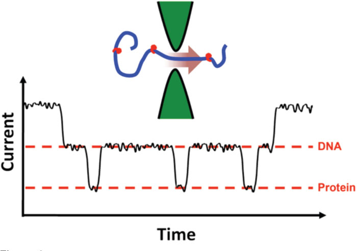
Figure 4: Local protein binding determination. A DNA molecule with attached proteins (a “beaded necklace” structure) can cause additional changes to the measured current within an event due to the brief, spatially-constrained effect of the proteins threading through the nanopore. In this measurement, the time domain maps to the length of the threading molecule, showing single-molecule “topography.” Not actual data.
Although much of the focus of solid-state nanopores has been on biosensing, some recent effort has been made to apply the same sensing technique to other nanoparticles. For instance, the translocation of both polystyrene [Reference Prabhu, Jubery, Freedman, Mulero, Dutta and Kim46] and gold nanoparticles [Reference Gierhart, Flowitt, Chen, Zhu, Kotecki, Smith and Collins47] has been studied, offering a method for measuring size variability or separation through size exclusion. Single-wall nanotubes (SWNT) have also been studied [Reference Hall, Keegstra, Duch, Hersam and Dekker48]. Although early measurements on this widely studied class of material demonstrated a means by which to monitor nanotube conglomeration, or “bundling,” the solid-state nanopore technique could be used to sort individual SWNT based on their diameter and thus their electrical properties [Reference Dresselhaus, Dresselhaus and Saito49].
Future Prospects
DNA sequencing remains the optimistic outcome of a great deal of solid-state nanopore research. However, our increasing understanding of the physics of nanopore detection has revealed difficulties with reading directly the nucleotide order from a single, continuously threading molecule. For instance, most membranes tend to be no less than 5 nm thick, meaning that several nucleotides are present within the nanopore at any given time and thus contribute to the instantaneous current in an integrative fashion. This has sparked interest in the use of alternative materials like graphene [Reference Garaj, Hubbard, Reina, Kong, Branton and Golovchenko50, Reference Merchant, Healy, Wanunu, Ray, Peterman, Bartel, Fischbein, Venta, Luo, Johnson and Drndic51, Reference Schneider, Kowalczyk, Calado, Pandraud, Zandbergen, Vandersypen and Dekker52] that can form atomically thin membranes. Currently, devices of this kind are in early stages of development, but show great potential. Another major consideration is the speed at which a molecule passes through the nanopore. In typical experiments, nucleotides are threaded at a rate of 107 bases per second [Reference Storm, Storm, Chen, Zandbergen, Joanny and Dekker32], and, even with optimized conditions [Reference Fologea, Uplinger, Thomas, McNabb and Li34, Reference Wanunu, Morrison, Rabin, Grosberg and Meller35, Reference Kowalczyk, Wells, Aksimentiev and Dekker38], this value can be reduced only by 1–2 orders of magnitude. Such speeds place severe requirements on electronic measurement bandwidth for the detection of small features. Therefore, recent studies have concentrated on combining solid-state nanopores with other single-molecule manipulation techniques such as optical tweezers [Reference Keyser, van der Does, Dekker and Dekker53] and magnetic tweezers [Reference Peng and Ling54] to control translocation speed arbitrarily or even halt and reverse it. Besides sequencing applications, these combined systems are also revealing a great deal about the basic science of nanopores [Reference Keyser, Dekker, Dekker and Lemay55].
While solid-state nanopores are being used to great effect, advances with biological nanopores continue as well. Therefore, there is recent interest in exploiting the advantages of both systems simultaneously by forming hybrid biological/solid-state devices. This has been demonstrated with alpha hemolysin nanopores [Reference Hall, Scott, Rotem, Mehta, Bayley and Dekker56] and more recently has been expanded to incorporate custom nanopores made using DNA origami [Reference Bell, Engst, Ablay, Divitini, Ducati, Liedl and Keyser57, Reference Wei, Martin, Rant and Dietz58].
Alternative techniques are also being pursued for accurate nanopore sequencing. One example uses a pre-treatment to amplify each individual nucleotide into a string of several copies [Reference McNally, Singer, Yu, Sun, Weng and Meller59], therefore requiring less spatial resolution. Another example incorporates small molecules that bind to specific short sequences of DNA, allowing spatial determination of identifying regions rather than individual nucleotides [Reference Singer, Rapireddy, Ly and Meller60]. Finally, several groups are pursuing nanopore devices with incorporated nanoelectrodes [Reference Huang, He, Chang, Zhang, Liang, Li, Tuchband, Fuhrmann, Ros and Lindsay61, Reference Ivanov, Instuli, McGilvery, Baldwin, McComb, Albrecht and Edel62, Reference Jiang, Mihovilovic, Chan and Stein63, Reference Sadki, Garaj, Vlassarev, Golovchenko and Branton64] to measure sequences using tunneling currents rather than trans-membrane ionic current. Each of these methods shows great potential for success. While the race is close, the finish line appears to be in sight.
Conclusion
Solid-state nanopores are gaining significant attention because of their potential as single-molecule detectors. As our understanding of this elegant but complex system deepens, the field inches closer to important applications in, for example, biomedical science. Advances with HIM fabrication may allow these goals to be realized even more rapidly.


