Introduction
Major developments in III-nitride semiconductors have led to the commercial production of InGaN/GaN light-emitting diodes [Reference Nakamura and Fasol1] and current injection violet lasers [Reference Nakamura and Fasol1,Reference Song, Shan and Edgar2]. In spite of its large threading dislocation densities, the InGaN/GaN system exhibits intense electroluminescence and photoluminescence (PL) [Reference Nakamura, Senoh, Nagahama, Iwasa, Yamada and Nukai3]. Two mechanisms have been suggested for these anomalous phenomena. First, the incorporation of In atoms could play a crucial role by suppressing nonradiative recombination rates, through the capture of carriers in localization centers originating from quantum dot-like and phase-separated In-rich regions [Reference Chichibu, Abare, Minsky, Keller, Fleisher, Bowers, Hu, Mishra, Coldren, Denbaars and Sota4,Reference Narukawa, Kawakami, Funato, Fujita, Fujita and Nakamura5]. Second, Narukawa et al. suggested that the incorporation of only 2% In into the GaN layer can effectively reduce the density of nonradiative recombination centers [Reference Narukawa, Saijou, Kawakami, Fujita, Mukai and Nakamura6]. However, systematic studies on the characteristics of InGaN/GaN MQWs with different In compositions are scarce. These studies are crucial not only for physical interest, but also for the design of practical optical devices.
We report a systematic study of both the structural and optical properties of InxGa1−xN/GaN MQWs by combining the results of high resolution x-ray diffraction (HRXRD), PL, and PL excitation (PLE) measurements. Stimulated emission (SE), temperature-dependent PL, and time-resolved PL (TRPL) measurements were also performed to evaluate the optical efficiencies of the MQWs and their device applicability. We used InGaN/GaN MQWs with different In compositions of 8.8, 12.0, and 13.3%. These samples have room temperature (RT) SE wavelengths ranging from 395 nm to 405 nm, which is close to the operational wavelength of state-of-the-art current injection violet lasers [Reference Song, Shan and Edgar2]. Therefore, understanding the physical mechanisms in these structures could give insight for increasing the operational wavelength of InGaN/GaN lasers.Through HRXRD analysis, we found that samples with higher In composition have a larger full width at half-maximum (FWHM) of superlattice (SL) peaks, indicating rougher interfaces. However, these samples have lower RT SE threshold densities and lower nonradiative recombination rates, as determined by SE and TRPL experiments. We attribute the lower RT SE threshold densities of the higher In composition samples to the suppression of nonradiative recombination, due to the incorporation of In.
Experimental Details
The set of InGaN/GaN MQW samples used in this study were grown on c-plane sapphire substrates by metalorganic chemical vapor deposition [Reference Keller, Abare, Minsky, Wu, Mack, Speck, Hu, Coldren, Mishra and Denbaars7]. The samples were nominally identical, apart from deliberate variations in the In composition of the InGaN well layer. The samples consisted of (i) a 2.5-µm-thick GaN buffer layer doped with Si at 3 × 1018 cm−3, (ii) a five-period SL of 3-nm-thick undoped InGaN wells and 7-nm-thick GaN barriers doped with Si at ∼5 × 1018 cm−3 to improve the interface properties [Reference Cho, Song, Keller, Minsky, Hu, Mishra and Denbaars8], and (iii) a 100-nm-thick GaN capping layer to prevent surface recombination. During the SL growth, the trimethylgallium and ammonia fluxes were held constant at 2.2 μmol/min and 0.32 mol/min. To obtain samples with different In compositions in the InGaN wells, trimethylindium (TMIn) fluxes of 13, 26, and 39 μmol/min were used for the different samples, while the InGaN well growth time was kept constant.
To evaluate the interface quality, the MQW average In composition, and the SL period, the samples were analyzed with HRXRD. PL and PLE experiments were performed using quasimonochromatic light dispersed by a ½ m monochromator from a xenon lamp. To examine the relevance of these MQWs to device applications, optically pumped SE experiments were performed at RT in the side-pumping geometry. The SE experimental details are reported elsewhere [Reference Bidnyk, Schmidt, Cho, Gainer, Song, Keller, Mishra and Denbaars9]. To check the temperature-dependent optical efficiencies of the MQWs, PL spectra were obtained as a function of temperature from 10 to 300 K using the 325 nm line of a cw He-Cd laser. Carrier lifetimes were measured by TRPL, using a streak camera for detection and a tunable picosecond pulsed laser system as an excitation source [Reference Cho, Song, Keller, Minsky, Hu, Mishra and Denbaars8].
Discussion
Figure 1 (a) shows the HRXRD diffraction pattern for the (0002) reflection from the five-period InxGa1−xN/GaN MQWs with different In compositions. The FWHM of SL-1 and SL-2 peaks are plotted as a function of In composition in Fig. 1 (b). The strongest peaks are from the GaN layers. SL satellite peaks are marked as SL-1, SL-2, and SL1. The zero-order SL peaks (SL0) appear as a low angle shoulder on the GaN peaks. All spectra clearly show higher-order SL diffraction peaks indicating good layer periodicity. Best fitting of the spectra in Fig. 1 (a) yields In compositions of 8.8%, 12.0%, and 13.3% for the samples with InGaN well layers grown with TMIn fluxes of 13, 26, and 39 µmol/min, respectively [Reference Cho, Song, Keller, Minsky, Hu, Mishra and Denbaars8]. As shown in Fig. 1 (a) and (b), with increasing In composition, the FWHM of the higher-order SL satellite peaks broadens. This broadening may be caused by spatial variation of the SL period (due to intermixing and/or well size irregularity) and/or alloy composition fluctuation [Reference Cho, Song, Keller, Minsky, Hu, Mishra and Denbaars8]. The degree of these fluctuations increases with increasing In composition. The large difference in interatomic spacing between GaN and InN, and the high equilibrium vapor pressure of InN may hinder the growth of InxGa1−xN, especially for higher In composition [Reference Singh, Doppalapudi, Moustakas and Romano10].
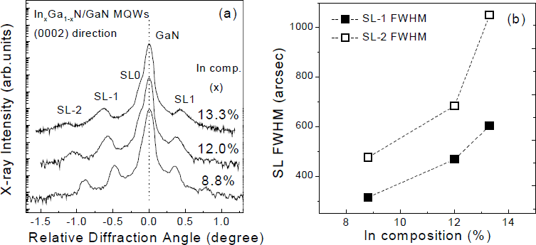
Figure 1 Five-period InxGa1−xN/GaN MQW (a) HRXRD diffraction pattern for the (0002) reflection and (b) FWHM of SL-1 and SL-2 peaks as a function of In composition. The lines in (b) are guides for the eye.
Figure 2 (a) shows 10 K PL and PLE spectra and (b) the corresponding Stokes shift and PLE bandedge broadening of the InGaN/GaN MQWs with different In compositions. The PLE detection energy is set at the main InGaN-related PL peak. With increasing In composition, the InGaN-related PLE bandedge redshifts and broadens. We obtained “effective band gap” Eeff values of 3.256, 3.207, and 3.165 eV and broadening ΔE values of 23, 36, and 40 meV, for the samples with In compositions of 8.8%, 12.0%, and 13.3%, respectively, by fitting the PLE spectra [Reference Martin, Middleton, O’Donnell and Van der Stricht11]. This broadening of PLE spectra with increasing In indicates that the absorption states are distributed over a wider energy range, due to an increase in the degree of fluctuations in dot size and/or shape [Reference Martin, Middleton, O’Donnell and Van der Stricht11], or due to an increase in interface imperfection as shown in Fig. 1. A large Stokes shift of the PL emission from the InGaN well with respect to the ’’effective band gap’’ measured by PLE is clearly observed. If we define the Stokes shift as the difference in energy between the PL peak energy and ’’effective band gap’’, Stokes’ shift increases at 135, 170, and 180 meV, respectively, as In composition increases. The large Stokes shifts and their increase with In composition can be explained by carrier localization [Reference Narukawa, Kawakami, Funato, Fujita, Fujita and Nakamura5] or the piezoelectric effect [Reference Kollmer, Im, Heppel, Off, Scholz and Hangleiter12], or a combined effect of both mechanisms [Reference Chichibu, Abare, Minsky, Keller, Fleisher, Bowers, Hu, Mishra, Coldren, Denbaars and Sota4].
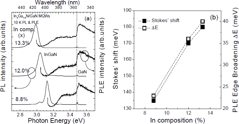
Figure 2 (a) 10 K PL and PLE spectra and (b) the corresponding Stokes shift and PLE bandedge broadening ΔE of the InGaN/GaN MQWs with different In compositions. The Stokes shift is the difference in energy between the PL peak energy and “effective band gap”Eeff. Eeff and ΔE values are obtained by fitting the PLE spectra. The lines in (b) are guides for the eye.
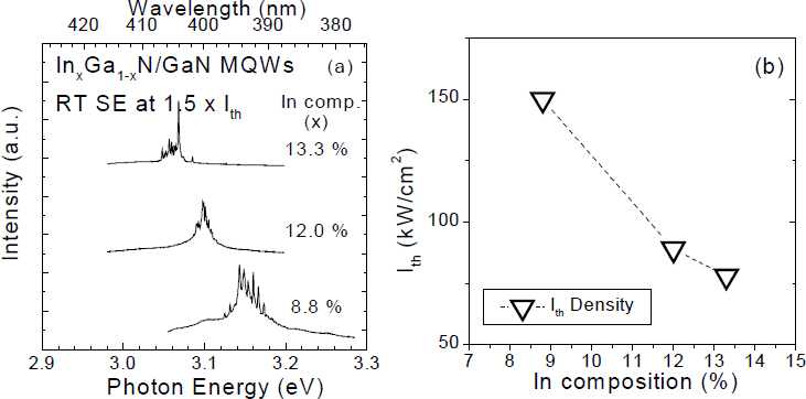
SE experiments at RT (the normal device operation temperature) were performed in order to compare the SE behavior of the InGaN/GaN MQWs with different In compositions. SE spectra shown in Fig. 3 (a) were obtained at a pump density of 1.5 × Ith, where Ith is the SE threshold. Ith is plotted as a function of In composition in Fig. 3 (b). Below Ith, the spontaneous emission peak blueshifted with increasing excitation power density due to the band filling of localized states or due to the screening of the piezoelectric field by the higher charge carrier density. As we further raise the excitation power density above Ith, a considerable spectral narrowing occurs, as shown in Fig. 3 (a) [Reference Bidnyk, Schmidt, Cho, Gainer, Song, Keller, Mishra and Denbaars9]. The SE threshold was 150, 89, and 78 kW/cm2, for the samples with In compositions of 8.8%, 12.0%, and 13.3%, respectively. It is interesting to note that the SE threshold decreases with increasing In composition, while the SL-1 and SL-2 FWHM and PLE bandedge broaden with increasing In composition, indicating the deterioration of interface quality due to the difficulty of achieving uniform In incorporation into GaN layers. This interface fluctuation causes scattering loss, and the absorption states distributed over a wider energy range broaden the gain spectrum. Both factors are disadvantageous to SE. However, a lower SE threshold density is observed for higher In composition. This is contrary to traditional III-V semiconductors such as GaAs and InP [Reference Sugiura, Mitsuhara, Oohashi, Hirono and Nakashima13]. The FWHM of the SL diffraction peaks is closely related to the optical quality of MQWs and the performance of devices using MQWs as an active layer for many other III-V semiconductor systems [Reference Sugiura, Mitsuhara, Oohashi, Hirono and Nakashima13].

Figure 3 (a) RT SE spectra and (b) the corresponding SE threshold pumping density Ith of the InGaN/GaN MQWs with different In compositions. The line in (b) is a guide for the eye.
To further investigate the optical efficiency and recombination dynamics of InGaN/GaN MQWs, temperature-dependent PL and TRPL measurements were performed. As the temperature was increased from 10 K to 300 K, the integrated PL intensity decreased by a factor of 25, 6, and 5 for the samples with 8.8%, 12.0%, and 13.3% In, respectively. The samples with a higher In composition are less sensitive to the increase in temperature, possibly due to less thermally activated nonradiative recombination. To clarify this, temperature-dependent carrier lifetimes were measured by TRPL, as shown in Figure 4 (b). In addition, the energy position dependent lifetime at 10 K is shown in Fig. 4 (a). At 10 K, the lifetime at the low-energy side of the InGaN peaks is longer for higher In composition, as expected from the larger Stokes shift [Reference Cho, Song, Keller, Minsky, Hu, Mishra and Denbaars8]. Below ∼50 K, the lifetimes increase with temperature, indicating that radiative recombination dominates in these samples at low temperatures. As the temperature is further increased, the lifetime decreases, since non-radiative processes predominantly influence the emission at higher temperatures. At RT, the samples have very different lifetimes because of different levels of thermally activated nonradiative recombination. From an analysis of the temperature dependence of the integrated PL intensities and carrier lifetimes, we extracted the RT nonradiative recombination lifetimes of 0.6, 2.7, and 3.6 ns for the 8.8%, 12.0%, and 13.3% In samples, respectively [Reference Narukawa, Saijou, Kawakami, Fujita, Mukai and Nakamura6]. These results are consistent with the temperature-dependent PL data and indicate the suppression of nonradiative recombination for higher In composition samples. The possible mechanism for these phenomena can be argued as follows. First, the effect of localization keeping carriers away from nonradiative pathways can be enhanced with increasing In, as shown in Fig. 2 (a) and (b) by the increase in Stokes shift with increasing In composition [Reference Chichibu, Abare, Minsky, Keller, Fleisher, Bowers, Hu, Mishra, Coldren, Denbaars and Sota4,Reference Narukawa, Kawakami, Funato, Fujita, Fujita and Nakamura5]. Second, the incorporation of more In into the InGaN well layer can reduce the density of nonradiative recombination centers [Reference Narukawa, Saijou, Kawakami, Fujita, Mukai and Nakamura6]. The RT SE threshold is lowered by suppressing nonradiative recombination, since only radiative recombination contributes to gain. In addition, a lower RT SE threshold for samples with higher In composition indicates that the suppression of nonradiative recombination overcomes the drawbacks associated with increasing interface imperfection.

Figure 4 (a) Energy-position dependent lifetime at 10 K and time-integrated PL spectra and (b) temperature-dependent lifetime of wavelength-integrated luminescence for the InGaN/GaN MQWs with different In compositions.
Conclusion
In summary, we investigated the effect of In on the structural and optical properties of InxGa1−xN/GaN MQWs and showed the relevance of these properties to device applications. As the In composition increases, the FWHM of SL x-ray diffraction peaks broadens due to the spatial fluctuation of interfaces. However, the RT SE threshold densities decrease, and this is attributed to the increased suppression of nonradiative recombination with increasing In composition. The explanation for these phenomena may be the role of In atoms in keeping carriers away from nonradiative pathways and/or in reducing the density of nonradiative recombination centers.
Acknowledgements
This work was supported by BMDO, AFOSR, NSF, and ONR.