


Introduction
Atomic force microscopy (AFM) has experienced a vast expansion of applications because it has been used to map not only topography but also a range of material properties. For mechanical characterization, modes such as PeakForce Quantitative Nanomechanics (QNM) and fast force volume (FFV) have not only made high-resolution mechanical mapping routine, but have also provided an entire force curve for every pixel of the image [Reference Pittenger1, Reference Pittenger and Yablon2]. For electrical characterization, a range of application modules is available, and even electrical measurements in liquid are possible with the recent introduction of insulated AFM nanoelectrode probes for scanning electrochemical microscopy (SECM) [Reference Nellist3, Reference Nellist4]. In the conventional approach, a fixed set of operating conditions (DC bias, AC bias, frequency, etc.) is used, and a single electrical measurement is performed for every XY location, yielding a 2D electrical map. This is also true in PeakForce Tunneling AFM (TUNA) [Reference Li5] and related PeakForce Tapping–based electrical modes, which overcome the limitations of contact mode. Aside from 2D maps, AFM-based electrical characterization has long included point spectroscopy, such as current-voltage (I-V) curves at individual points or in arrays, for studying pn-junction delineation in Si devices [Reference Edwards6] and for investigating humidity effects on nanoscale electrochemistry in solid silver ion conductors [Reference Yang7].
In this article, we describe a set of new electrical data-cube (DCUBE) modes that combine imaging and point spectroscopy, producing an integrated 3D data set. Thus, the subjective approach of guessing locations of interest (for single-point spectroscopy) is replaced by a big-data approach resulting in higher dimensional data that can be sliced along any axis or plane and is conducive to principal component analysis and machine learning approaches to data reduction. Rather than employing contact mode, spectrum acquisition is embedded in the hold segment of a force curve that is part of a FFV map (see Figure 1) [Reference Pittenger and Yablon8], using a patented low-force trigger capability to maintain regular imaging speeds with force ramp rates up to 300 Hz and sub-100 ms dwell times for the hold segment. The force curve at every pixel embedded in the FFV map constitutes a set of nanomechanical data cubes acquired simultaneously, which are spatially correlated with the electrical data cubes. Since the FFV map avoids lateral forces, this approach also extends electrical measurements to polymers, nanoparticles, and other fragile samples that are impossible to study in contact mode.
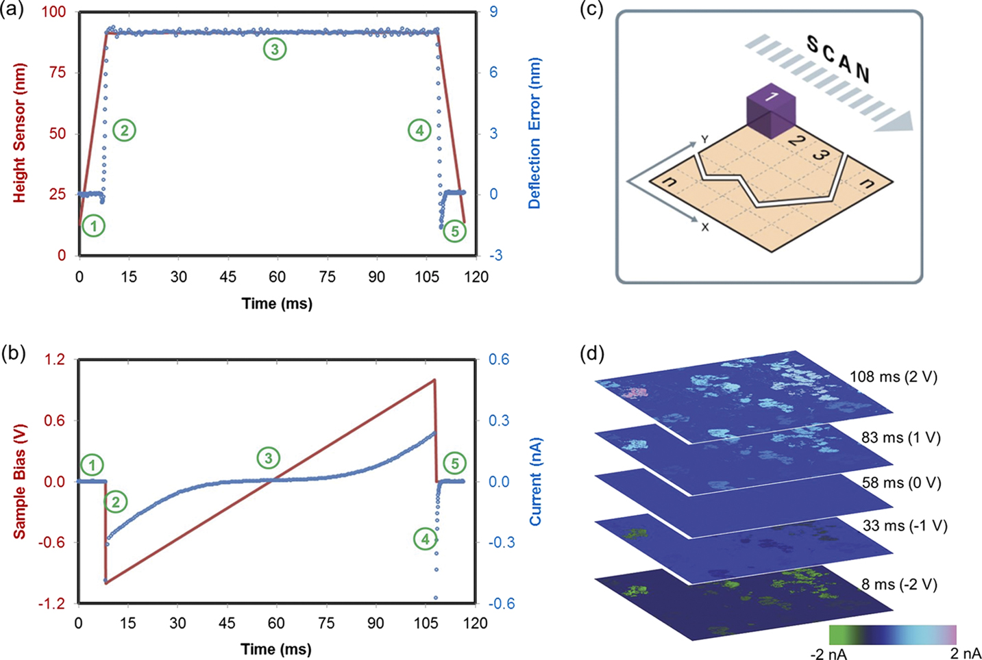
Figure 1 Data cube (DCUBE) modes operating on fast force volume (FFV) approach: (a) height sensor (red) and deflection error (blue open circle) plots with segments showing extend (1–2), dwell (3), and retract (4–5) cycles; (b) pattern of sample bias (red) and corresponding tunneling AFM (TUNA) current (blue); (c) illustration of scan pattern during acquisition of DCUBE-mode data; and (d) five TUNA current slices from the DCUBE-TUNA results.
This approach is general. All measurable electrical parameters can be ramped (for example, DC bias or frequency), and time-dependent phenomena can be studied. Applicable electrical modes include conductive and tunneling AFM (DCUBE-TUNA) [Reference Li5], scanning capacitance microscopy (DCUBE-SCM) [Reference De Wolf9], scanning spreading resistance microscopy (DCUBE-SSRM), scanning microwave impedance microscopy (DCUBE-sMIM) [Reference Huang10], piezoresponse force microscopy (DCUBE-PFM) [Reference Calahorra11], and contact resonance piezoresponse force microscopy (DCUBE-CR-PFM). The resultant data can not only be analyzed as a set of spatial images, spatio-spectral slices, or point spectra, but they represent a complete multidimensional data set.
The sections below describe six data-cube (DCUBE) modes. The figures related to these modes illustrate various ways of extracting and presenting data from the data-cube.
Barrier Height Mapping with DCUBE-TUNA
For this study, a data cube containing a tunneling AFM (DCUBE-TUNA) data set was acquired on a thin film of maghemite (γ-Fe2O3), a material with applications ranging from data storage to biomedicine. As shown in Figure 2, the topography (2a), the concurrent acquisition of adhesion strength (2b), and electrical information (2c) show the presence of several particle types with distinct adhesion behavior and a range of conductivities. The single current slice shown in Figure 2c represents all that would be available in a conventional conductivity map. From this data-cube mode, an entire stack of images can be extracted spanning bias voltages from -2V to +2V. Doing so shows the presence of additional domains that are not apparent in a single electrical slice, or in the topography or adhesion channels. Further, analysis of a sub-space of the data cube, such as I-V curves, and presentation of the extracted data in a density plot (2d) reveals that three primary types of curves are present. For further analysis and data reduction, the data cube was imported into MATLAB, where the I-V spectrum at each pixel was fit to a thermionic emission model to determine the Schottky barrier height at the metal tip / γ-Fe2O3 semiconductor junction for each location. The result is shown in Figure 2e. Here the color bar represents a barrier ranging from zero (ohmic behavior) to one (insulator). This result confirms previous PeakForce TUNA and sMIM studies showing that for this sample distinct electrical properties exist at the particle level [Reference Huang10].
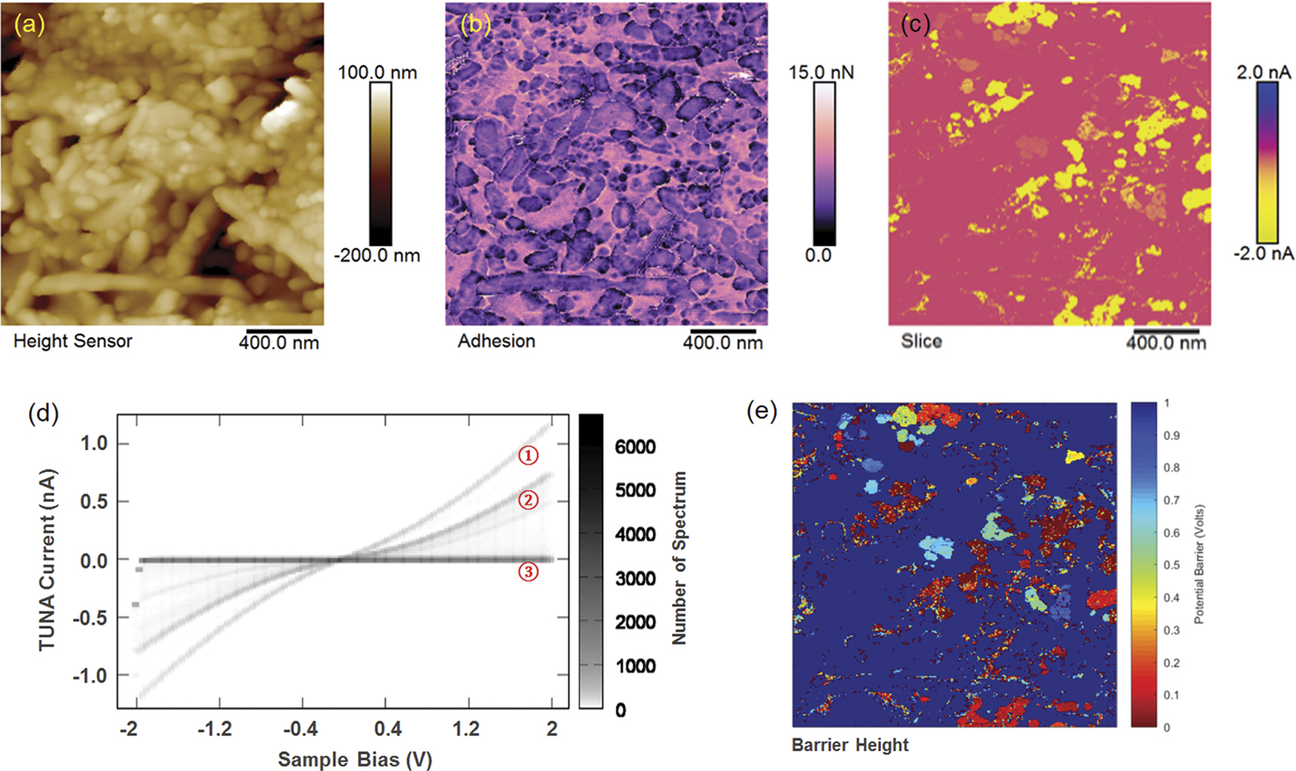
Figure 2 DCUBE tunneling AFM (TUNA) data from γ-Fe2O3: (a) surface topography; (b) adhesion map extracted from the fast force volume (FFV) data; (c) TUNA current slice at -1V bias; (d) density plot with color indicating the frequency of a given current-bias pair; and (e) scanning barrier height image created by analysis of each local I-V spectrum.
Li-ion Battery Cathode Characterization with DCUBE-TUNA
AFM has been a powerful tool for battery studies. A battery system integrates materials with distinct mechanical properties, from soft (polymer additive) and loose (conductive additive) to hard (Li metal oxide) and porous (separator) surfaces [Reference Palacin and de Guibert12]. Significant variation in surface topography and properties is also common for battery electrodes and poses challenges for conventional AFM electrical modes that operate in contact mode. The high normal and shear forces of contact mode lead to sample damage and AFM tip fouling, which limits resolution and reproducibility. For this reason PeakForce Tapping and its nanoelectrical variants, such as PeakForce TUNA [Reference Li5], have played an important role in AFM-based battery research in recent years [Reference Liu13]. Here, the added advantages of DCUBE-TUNA are illustrated on a battery cathode consisting of Li metal oxide, polymer binder, and conductive carbon nanoparticles.
Figure 3 shows 15 µm × 15 µm images extracted from a DCUBE-TUNA data set. A few large Li metal oxide grains are easily seen in topography and are marked as areas 1–3 in panel 3a. The modulus image (3b) identifies the interstitial material as mostly soft polymer binder. Closer inspection of Figure 3b shows variation in the softer material, which correlates with the conductivity map in Figures 3c and 3d. Regions of high conductivity where carbon black particles are embedded in the binder material are clearly differentiated. This is in line with expectations, given prior knowledge of this cathode’s constituents. Interestingly, the conductivity image (3c) also shows that the grain marked as number 2 is “dead.” It shows no measurable conductivity over the entire -3.5 V to +4 V bias range represented by the image slices extracted in Figure 3e. This could be an issue of the carbon black additive distribution having failed to provide a conductive channel (no evidence of carbon black is seen near this grain in the conductivity maps), or it could be the nature of this metal oxide grain itself. In a practical battery, “dead” grains are to be avoided as they lower available specific and volumetric energy density without a concomitant increase in lifetime or power density. Thus, DCUBE-TUNA enables new battery cathode studies. The resulting reproducible, multidimensional data set not only allows dissection of the spatial component distribution, it also can uncover the presence of “dead” metal oxide grains.
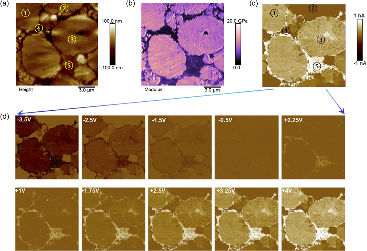
Figure 3 DCUBE tunneling AFM (TUNA) studies of a battery cathode: (a) surface topography with typical features showing domains of Li metal oxide (1–3), polymer binder (4), and carbon black (5); (b) quantitative elastic modulus map differentiating domains; (c) a slice of the TUNA current data cube at +4 V; and (d) a collection of slices at select biases. All data acquired in a single scan.
Active Carrier Profiling with DCUBE-SCM
Scanning capacitance microscopy (SCM) provides a method for profiling carrier concentration with nanometer-scale resolution in two dimensions [Reference De Wolf9]. Applications of SCM include failure analysis and 2D carrier profiling of semiconductor devices. Traditional SCM has two well-known issues. One, it is based on contact mode and thus suffers from typical issues of high normal and shear forces. The other is the limited information content available at fixed DC bias. The data cube approach addresses both issues, giving additional insight into device properties, such as effective gate channel length and defects.
Figure 4 shows dC/dV amplitude data extracted from a DCUBE-SCM data set of two adjacent static random-access memory (SRAM) transistors. The spatio-spectral slices in Figures 4a and 4b highlight the evolution of the junction profile with increasing DC bias. This allows visualization of the apparent junction with its true effective gate channel length as a function of applied bias. Figures 4c–4g show image slices at various fixed DC bias values. Some of these slices show that the transistor on the right has a defect that shows up at certain bias values, which would have been easily missed in a conventional SCM image at a single bias.
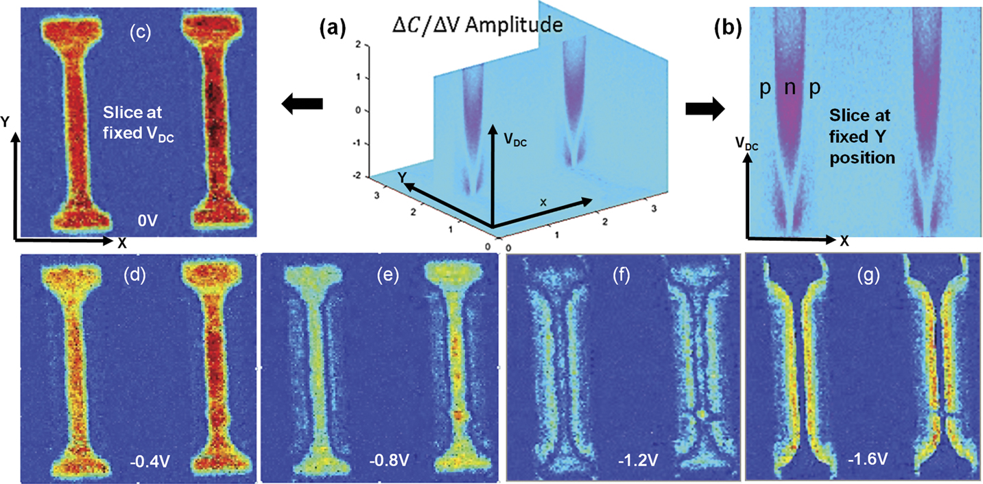
Figure 4 DCUBE scanning capacitance microscopy (SCM) studies of a SRAM transistor: (a) data cube in a 3D space of X, Y and Vdc; (b) a slice of the data cube at a fixed Y position; and (c)–(g) slices at select, fixed DC biases along the Vdc coordinate.
Impedance Microscopy with DCUBE-sMIM
Scanning microwave impedance microscopy (sMIM) is an AFM-based near-field optical technique for materials and device characterization [Reference Huang10]. The sMIM mode creates maps not only of dC/dV (as does SCM), but also maps of nonlinear resistivity dR/dV, as well as variations in absolute permittivity (capacitive signal, sMIM-C) and conductivity (resistive signal, sMIM-R) of the material. Again, DCUBE-sMIM improves on traditional sMIM mode by avoiding the use of contact mode. It further reveals additional information, such as conduction type, oxide thickness, oxide surface charges, contamination from mobile ions, and interface trap density.
Figure 5 shows data extracted from a DCUBE-sMIM study of a Si sample with n-type and p-type staircase carrier profiles, obtained from Infineon Technologies. In this study, both the C-V (sMIM-C vs sample bias) and R-V (sMIM-R vs sample bias) were collected within 100 ms per pixel, covering a bias range of -2 V to 2 V. Having images over this bias range helps in differentiating and locating all regions and carrier levels in the sample. This is seen in the sMIM-C data of Figures 5a–5c, where the negative bias in Figure 5a drives the n-type regions into the depletion regime, enhancing their contrast, while p-type regions are in the inversion regime, depressing their contrast. The positive bias in Figure 5c has the opposite effect. Figures 5d–5f show force, R-V, and C-V spectra on the locations marked by X in Figure 5b. Figure 5g combines bias-dependent sMIM-C and sMIM-R signals with pixel-wise location information into a single spatio-spectral slice.
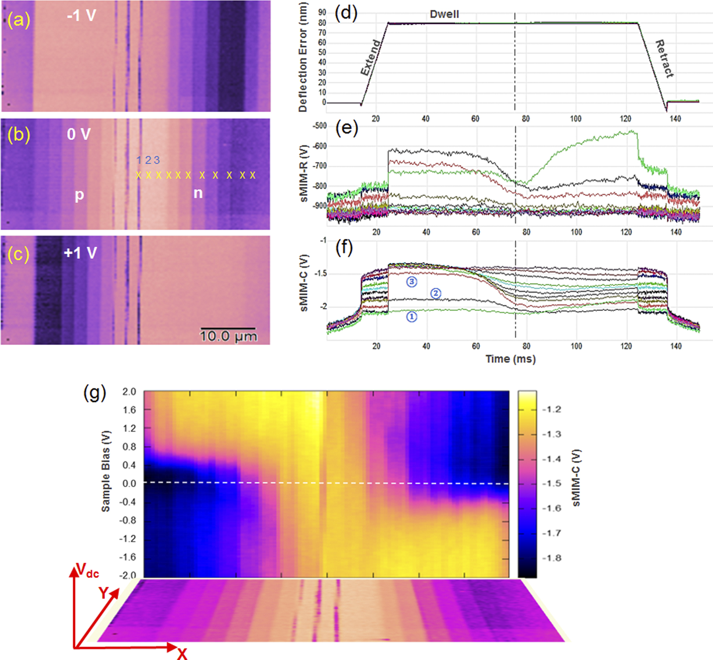
Figure 5 DCUBE scanning microwave impedance microscopy (sMIM) study of a Si sample with n-type and p-type staircase carrier profile: (a)–(c) slices of carrier profiles at selected sample biases; (d)–(f) eleven spectral sets of force, sMIM-R and sMIM-C, respectively, user-selected from the X-marked point locations on (b); and (g) a slice image representing the sMIM-C signal versus sample bias and X position at a fixed Y location.
Moreover, DCUBE-sMIM provides valuable nanoelectrical information both during the surface hold time and during the approach and retract processes. This is seen in Figures 5e and 5f, which are spectra taken at the locations marked by X in Figure 5b. First, during the hold time, the sMIM-C signal in Figure 5e shows a gradual change in slope with carrier density. Most curves were taken in the n-type region. At negative bias, this region is in the accumulation regime, causing equally high sMIM-C signal, which then drops as the bias turns positive and the sample goes into depletion. The signal drops further for lower doped regions. Second, Figures 5e and 5f also capture the sMIM signals before the probe touches and before bias is applied, automatically capturing the distance dependence. Fitting of the sMIM-C versus distance spectra allows one to extract tip-shape information, while subtraction of signal background is a path for quantification of the sMIM-C signal. Detailed analysis and comparison of the sMIM signal during the “extend” and “retract” period also provides important information. For example, asymmetric behaviors indicate a change of the sample surface after the dwell time. This is likely since the voltage sweeping rate is slow to avoid unwanted charge accumulation, and one can observe the spectral feature of the quasi-static capacitance.
Domain-Switching Dynamics with DCUBE-PFM
Piezoresponse force microscopy (PFM) has been widely used for domain writing and ferroelectric switching studies [Reference Wang14]. Traditionally, PFM is performed in contact mode, using a lock-in amplifier to measure cantilever AC deflection. Use of DCUBE-PFM enables simultaneous acquisition of nanomechanical mapping along with PFM amplitude and phase spectra in every pixel. The PFM spectra reveal the switching voltage of each individual domain in a single data set. In addition, DCUBE-PFM overcomes artifacts, tip wear, sample damage, and the complexity of data analysis associated with conventional contact mode approaches.
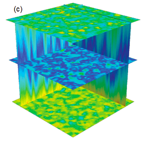
Piezoelectric poling dynamics vary by domain. The study of a thin film of BiFeO3 (BFO) and individual spectra of amplitude and phase give an indication of the variability. This can be seen in Figures 6a and 6b, where the switching voltage, as shown in the minimum of piezoelectric amplitude (6a) or the phase flip (6b), varies from spectrum to spectrum. While the spectra fall roughly into two groups, there is an obvious additional variation. These spectra are part of a 128 × 128 × 833 (or 1 µm × 1 µm × 6 V) DCUBE-PFM data set that is visualized more completely in Figure 6c (amplitude) and 6d (phase) using Mayavi software [Reference Ramachandran and Varoquaux15], as well as in Figures 6e to 6n, where 5 image slices of PFM amplitude (e–i) and 5 image slices of PFM phase (j–n) are extracted. Here we see that the spectral variation seen in 6a and 6b was not a question of reproducibility, but rather clear spatial variation, domain to domain, as well as within domains where phase flipping appears to occur from the boundary inward.
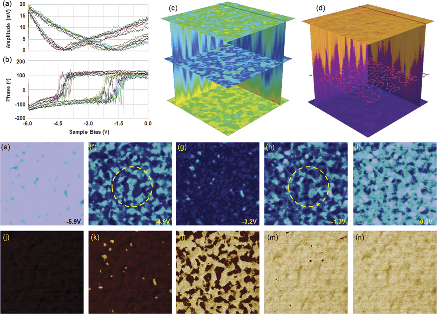
Figure 6 DCUBE piezoresponse force microscopy (PFM) studies of a BiFeO3 (BFO) piezoelectric film: (a) amplitude spectra; (b) corresponding phase spectra; (c) and (d) amplitude and phase cubes; (e)–(i) slices of amplitude at different sample bias; and (j)–(n) slices of phase at different sample bias.
High-Sensitivity Piezoelectric Mapping with DCUBE-CR-PFM
In PFM, applying an AC bias of a certain frequency results in a periodic deformation of the sample surface at the same frequency, which in turn drives a periodic deformation of the cantilever. The frequency can be chosen to coincide with the contact resonance of the cantilever-sample system, thus providing a signal enhancement on the order of the Q-factor, and this has been exploited in PFM to provide enhanced piezoelectric response signal [Reference Harnagea16]. The contact resonance frequency and Q-factor exhibit a strong dependence on contact stiffness, which is the basis of contact resonance imaging as a nanomechanical tool. Because of this dependence on the properties of a material phase, a single frequency is not sufficient for performing resonant-enhanced PFM on a heterogeneous (multiphase) sample.
DCUBE-CR-PFM addresses the aforementioned challenge by performing a fast frequency sweep during the surface dwell time to detect the number of contact resonance eigenmodes for every image pixel. This provides at the same time the following signals: a PFM signal enhancement and a complete nanomechanical characterization, including storage modulus, loss modulus, and adhesion, which can be determined from the contact resonance spectrum and the force curve. Figure 7 shows a DCUBE-CR-PFM data set of a LiTaO3 sample spanning a 3 µm × 3 µm × 150 kHz range. Figures 7a–7c are typical force, PFM phase, and PFM amplitude spectra, respectively, captured on two different domains. The variation of contact resonance with location is apparent in Figures 7d and e where sliding the image plane along the frequency axis highlights areas with enhancement at the same frequency. Figures 7h, 7i, and 7j show the strongest deviations in contact resonance frequency, amplitude, and Q-factor, and thus, viscoelastic properties for dark spots that correlate with elevations in topography may be surface adsorbates. The smaller contrast difference observed between phases is a result of the opposite poling in canceling vertical tip motion, leading to an effective reduction in drive amplitude at those locations, as indicated in Figure 7g.
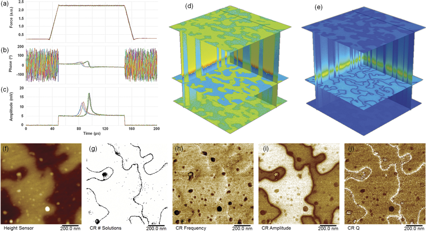
Figure 7 DCUBE contact resonance piezoresponse force microscopy (CR-PFM) studies on a LiTaO3 sample: (a)–(c) typical DCUBE-CR PFM force ramping, PFM phase, and PFM amplitude spectra, respectively, with frequency swept from 250 to 400kHz; (d)–(e) phase and amplitude data cubes; (f) surface topography; (g) contact resonance solution; and (h)–(i) contact resonance frequency, amplitude, and quality factor.
Conclusion
Data cube–based electrical AFM modes represent a big-data approach to property measurements with the potential to provide new information in a wide range of applications, especially on samples with high complexity (multiple phases). Extracting image slices, spatio-spectral slices, or spectra at every pixel opens the door to new data reduction methods and analyses. This has been illustrated with the following examples: determining the local barrier height to current flow, uncovering intra-grain heterogeneity in battery cathodes and defects in semiconductor devices, determining the effective transistor gate length as a function of operating conditions, quantifying microwave impedance signals, and mapping single-domain piezoelectric switching dynamics and mechanical properties. It seems clear that AFM data cube capabilities will have an impact across a wide range of nanoelectrical characterization and research topics.


