Introduction
Energy-dispersive X-ray spectroscopy (EDS) is the method of choice for elemental microanalysis in the scanning electron microscope (SEM) and transmission electron microscope (TEM). It offers fast, easy-to-interpret information on constituent elements (qualitative analysis), composition (quantitative analysis), and elemental distribution (X-ray mapping) for most materials and applications. The development and utilization of the field emission gun (FEG) over the past 25 years has significantly improved the spatial resolution and therefore minimum feature size detectable in the SEM. Nano-characterization, defined here as the analysis of sub-100 nm features and structures, is now routine. The latest ultra-high-resolution FEG-SEMs promise examination of structures in the sub-10 nm regime using very low-beam energies (100–1,000 eV), and within-lens electron detectors. These developments have closed a performance gap with TEM and surface science tools, such as Auger, secondary ion mass spectrometry (SIMS), and X-ray photoelectron spectroscopy (XPS). This is timely because it coincides with the explosion of characterization requirements driven by developments in the fields of nano-technology and nano-science. Most EDS systems are only useful down to accelerating voltages where subsurface beam scattering limits the spatial resolution to 30 nm or greater. This means that a performance gap remains in SEM: samples can be imaged at nanometer resolution, but elemental analysis is still restricted to much larger regions.
In this article we look at the potential of new windowless silicon drift detector (SDD) EDS detectors, with more efficient geometry and low-noise electronics that significantly enhance sensitivity to low-energy X-rays. We also consider how the capability to detect low-energy X-rays offers potential for enhancing the spatial resolution and surface sensitivity of elemental analysis, as well as improving light element characterization in the SEM.
Materials and Methods
Challenges of low-energy X-ray analysis
The most direct method for improving the spatial resolution of EDS analysis in bulk specimens is by reducing the electron accelerating voltage. This improvement comes about by reducing the size of the X-ray generation volume (Figure 1). However, EDS spatial resolution can still be on the order of 50–100 nm at 5 kV. To reduce interaction to the sub-20 nm level requires accelerating voltages of 2 kV or less for many (particularly low-density) materials. This has been the promise for improving spatial resolution since the early days of FEG-SEM [Reference Barkshire1], however, the barriers to practical analysis increase as the accelerating voltage is reduced.

Figure 1 Monte Carlo simulations at 3, 1.5, and 1 kV for pure iron (7.9 gm/cm3). Black trajectories show the total extent of electron penetration, and red trajectories indicate where electrons have sufficient energy to excite Fe L X-rays. Sub-10 nm spatial resolution is possible in this material if 1 kV can be used.
Figure 2 shows that as depth resolution improves with reduced accelerating voltage, the relative net count rates for the K-series of iron also decreases [Reference Pinard2]. This highlights two issues. Firstly, the K-series is only well excited at high kV (for example, 20 kV) and has low intensity at 10 kV. Secondly, below 7 kV only the less reliable L-series is excited, and its intensity also decreases rapidly as the accelerating voltage is reduced. At 2 kV the intensity of Fe L is around 35× smaller than Fe K intensity generated at 20 kV. Furthermore, a low accelerating voltage for high spatial resolution also means a small beam current, often measured in 10s or 100s of pA, thus further reducing the X-ray count rate.

Figure 2 X-ray emission depths or X-ray range (solid lines) and net intensity of the Fe K–L3 and L3–M4 and M5 X-ray transitions (dotted lines) as a function of the accelerating voltage [Reference Pinard2]. The range was calculated as the depth where 95% of the X-rays are emitted. The vertical dash lines indicate the critical ionization energy (Ec) of each X-ray transition.
The largest conventional EDS detectors offer up to 15× the sensitivity of the 10 mm2 detectors that were typically used on a tungsten filament SEM (W-SEM) before the introduction of the SDD. This goes someway to offset this count-rate deficit, however even the largest conventional detectors are only practical for analysis down to about 3 kV accelerating voltage, which corresponds to 30–50 nm spatial resolution (Figure 1).
Hardware developments for low-kV elemental analysis
Space constraints limit the practical size and distance from the specimen of even SDD sensors. Therefore to improve sensitivity, other methods have been investigated. One way to improve X-ray intensity for low-energy lines is to remove the X-ray window from the front of the detector. Although windowless SDD detectors have been available for TEM, removing the window presents design challenges for the SEM because of the potential for contamination of the sensor at poorer vacuum levels and the higher frequency of chamber venting. However, compared to liquid-nitrogen-cooled Si(Li) detectors, SDD detectors can operate at much higher temperatures, and the thermoelectric cooling employed offers much faster sensor warming and cooling. The detector therefore can be switched off automatically either by interlocking the pump/vent cycle of the microscope or by sensing changes in vacuum at the detector. Provided the electronics for the detector are designed to achieve signal-measurement stability very rapidly after cool down, a windowless SDD can be warmed up for specimen exchange and be back in operation within minutes. Removing the window removes the absorbing effects of the window material and also the obscuring effect of the grid structure that supports a thin window. The typical benefits of this for a windowless design versus a grid-supported polymer window can be seen in Table 1. For microanalysis using K lines at high kV, count rates with a windowless detector can be up to 50% higher. For low kV EDS, count rate increases for lines less than 1 keV are greater, with typical improvements about 2–3×. For very-low X-ray energies (sub-100 eV), improvements rise rapidly, making practical the detectability of low-energy L-lines of Si, Al, and Mg, and even the K-line of Li. The Si L and Al L lines are particularly important because their K lines are not usefully excited below 2 kV, and they are common constituents of many nano-materials.
Table 1 Improvement in count rate for selected X-ray lines with a windowless detector design versus a conventional detector with an AP3-type polymer window.
Removing the window is not sufficient for successful low-energy EDS because the very low-energy photons still must be detected and measured. The efficiency of a conventional electronics counting chain (detector and pulse processor) is unlikely to be good enough for extremely low-energy X-rays. Low-energy noise has to be minimized and signal processing must be optimized to separate from noise the lowest energy X-rays such as Li K and Al L (Figure 3).

Figure 3 X-ray spectra of Al metal with its native oxide taken at 2 kV using two windowless EDS detectors. The spectrum in yellow is with the new low-noise electronics and that in red is with standard electronics.
One potential additional benefit of removing the window is the saving of space, allowing the sensor to be moved closer to the sample. Thus, a further improvement in sensitivity can be achieved by using an oval-shaped sensor instead of a circular device. This allows a detector of the same large area to be positioned closer to the sample without touching a conical pole-piece (Figure 4). Using an oval-shaped design in a windowless configuration, solid angles over 0.2 sr have been achieved in practice on FEG-SEMs. Taking into account windowless operation and solid angle improvements, increases in count rate of around 75–100× have been achieved versus a conventional 10 mm2 SDD detector, and between 5–10× versus a 150 mm2 SDD detector for the N K line. Figure 5 compares spectra for CaSO4, collected at 3 kV under identical conditions, from a 100 mm2 windowless detector and a conventional 150 mm2 windowed detector. The increase in sensitivity is clear; the Ca L lines, heavily absorbed by a polymer window, are easily detected with the windowless detector.

Figure 4 Schematic diagram showing the difference in geometry between a windowless detector with a non-circular sensor and a circular large-area SDD detector. A conventional detector with a circular sensor operates at a longer working distance and further from the sample.

Figure 5 Spectra collected at 3 kV from CaSO4 using a windowless 100 mm2 detector (X-Max Extreme - red) compared to a 150 mm2 detector (X-MaxN150 - yellow) with polymer window at an identical take-off angle on the same SEM. The windowless design shows significant improvement in intensity. For example, the Ca L-series is indistinct using the conventional detector because of strong absorption in the polymer window.
One final, critical design issue for low kV EDS on the SEM is analytical working distance, that is, the microscope working distance at which EDS is practical. Conventional EDS-detector working distances have been relatively short for FE-SEM, in the range of 5–15 mm. However, when operating at sub-3 kV accelerating voltage, working distance must be reduced further for two reasons. Firstly, the beam size increases with working distance [Reference Goldstein3], and many microscopes are specified at about 1 mm for best resolution at 1 kV. Secondly, the contrast of within-lens secondary, and particularly backscatter, signals decreases rapidly with increasing working distance; optimal is normally 5 mm or less. Therefore, a further barrier to low-energy EDS is the need to work at short working distance to achieve sufficient image resolution and contrast. A further benefit of using an oval-shaped sensor is that the detector can often be designed to work at working distances in the range of 3–5 mm, about half that of a conventional detector. Again, this can be seen in the schematic representation of this design versus a conventional circular EDS detector shown in Figure 4.
X-ray lines for low-energy analysis
Conventional microanalysis at 20 kV or higher uses K lines for most common elements in metals, oxide ceramics, and minerals up to and including the first-row transition elements. For heavier elements L or M lines are typically used. Low-energy X-ray analysis requires the use of a very different collection of X-ray lines, using K lines for only the lightest elements and making use of low-energy L, M, and even N lines for other elements. Low-energy lines (< 1 keV) present a number of challenges for EDS including the following: low intensity, poor peak-to-background, poorly understood X-ray absorption (including self-absorption), and transitions from valence electrons, meaning line positions and intensities may change depending on the bonding environment of the constituent elements.
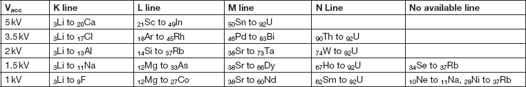
Table 2 shows the highest-energy X-ray line series available for EDS analysis at different accelerating voltages in the range 1–5 kV. Only at 5 kV can all naturally occurring elements be detected using K, L, or M lines, and this requires using L lines for first-row transition elements. At 3 kV, N lines are required for Th and U, and elements such as Sn require low-energy M lines. At 2 kV a line for every element may be detectable, although some like Si Ll at 92eV require the most sensitive detectors, and further effort is required to achieve accurate spectrum processing of these lines [Reference Burgess4]. Increasing interest in N lines (Figure 6) [Reference Burgess5] is being driven by their potential use for detecting some important heavy elements (for example, Ta and W) in semiconductor devices and superalloys. Even at 1 kV, where EDS spatial resolution is often significantly less than 10 nm, and surface analysis becomes possible, the majority of elements still emit characteristic X-rays giving the possibility for some elemental characterization (Table 2).

Figure 6 Spectra collected with a 100 m2 windowless detector (X-Max Extreme) at 3 kV for metals in the sixth row of the periodic table. Note the N lines detected for Bi (135 eV), Hf (200 eV), Ta (205 eV), W (21 eV), Ir (235 eV), Pt (245 eV), and Au (250 eV). Samples were plasma-cleaned for 30 minutes but show variable intensities of the C Kα peak, which makes particular contributions to the Ir N, Pt N, and Au N peaks.
Table 2 Highest-energy X-ray lines available for elements at different accelerating voltages from 5 kV–1 kV. As accelerating voltage is decreased, the highest-energy available lines will be lower in energy with reduced intensity and reduced peak-to-background. Even at 1 kV characteristic lines may be excited for most elements.

Results
The hardware solutions for low-energy X-ray analysis described above indicate that more low-energy X-ray lines are becoming accessible. These lines may not be as reliable for analysis as high-energy lines, but they do offer the potential for elemental analysis in applications and materials where previously no elemental information was attainable in the SEM. We now consider some applications that indicate the potential of a detector optimized for low-energy sensitivity: high spatial resolution nano-analysis, surface analysis, light element analysis, and lithium detection.
High spatial resolution analysis
Low accelerating voltage imaging of nano-particles using within-lens detectors shows detailed topographical information and atomic-number contrast. Figure 7 shows the analysis of ceramic oxide nano-particles (20–80 nm) formed by the sparking of ferrocerium on a silicon substrate [Reference Zhou6]. The backscatter image (Figure 7b) shows three distinct gray levels suggesting the existence of three phases of differing mean atomic number within these particles. To achieve the necessary spatial resolution, X-ray maps were collected at an accelerating voltage of 2 kV. The composite map (Figure 7c) confirms that three distinct oxide phases are present: the darkest, a MgZn oxide; medium-gray-level Fe oxide; and the brightest, an LaCe oxide. The elemental distribution was shown down to sub-10 nm scale with an acquisition time of 5 minutes.

Figure 7 Nanoparticles produced during sparking of ferrocerium [Reference Zhou6]. (a) SE image and (b) BSE image that shows strong material contrast variation within the particles indicating that each particle is composed of multiple phases. Images were collected using a Zeiss GeminiSEM500 at 2 kV beam energy with InLens (SE) and EsB (BSE) electron detectors. (c) Composite EDS layered element map of ferrocerium particles showing iron (yellow), lanthanum and cerium (green), magnesium and zinc (magenta), and silicon (blue) superimposed on a BSE image.
Additively manufactured Alloy 718 is a superalloy containing a range of precipitates of different sizes [Reference Bertali7]. It contains disk-shaped Ni3(Nb,Ti) γ” precipitates on the order of 10–15 nm in thickness in a matrix mainly of Cr, Fe, and Ni (Figure 8). Spectra collected at 3 and 1.5 kV from these precipitates and surrounding matrices demonstrate the improvement in spatial resolution achieved by reducing the accelerating voltage. In the 1.5 kV spectrum (Figure 8c), the Nb Mζ, and Ti L signals are clearer than the corresponding Nb L or Ti L signals in the 3.5 kV spectrum (Figure 8b). Note even at 1.5 kV that Fe and Cr are in the spectrum collected from the precipitate, showing that the X-ray generation region is not solely contained within the precipitate. A spectrum image dataset collected from an area containing these Ni3Nb γ” precipitates (Figure 8d) demonstrates that it is still practical to study elemental distribution of features on this scale using X-ray maps collected at 1.5 kV.

Figure 8 Fine-scale microstructure of Ni3Nb γ” precipitate grains in an Alloy 718 sample. (a) Within-lens BSE image (Zeiss Merlin ESB), (b) spectra collected from a γ” precipitate and adjacent Fe-Cr-rich matrix using 3 kV accelerating voltage; and (c) spectra collected from a γ” precipitate and adjacent matrix at 1.5 kV accelerating voltage. The γ” precipitate is enriched in Ni and also contains Nb and Ti. (d) Composite EDS layered element map of N, O, Fe, Cr, and Nb showing Al2O3, NbTiCN, and Ni3Nb γ” precipitates collected at 1.5 kV using an FEI Magellan SEM. Ni3Nb γ” precipitates are 30 nm long and less than 10 nm in width. Sample and data courtesy of A. Janssen and M.G. Burke, Materials Performance Centre, The University of Manchester.
Surface analysis
As shown in Figure 1, by reducing the accelerating voltage to very low values, the interaction volume of the electron beam is concentrated in the top few nm of a material. This is used in electron imaging to identify surface features such as in complex semiconductor structures (Figure 9). By reducing the accelerating voltage from 3 to 1 kV, the surface selectivity of the data improves, and imaging contrast is more clearly related to those structures on the sample surface. Collecting X-ray data under the same conditions makes the determination of what constitutes the surface of a complex structure, such as in this sample, much clearer [Reference Sagar8]. For example the X-ray maps for O K and Si L reveal where these elements are on the surface when collected at 1 kV, in contrast to the O K and Si K maps collected at 3 kV where elemental information from subsurface layers contributes significantly to the signal. In the case of Ti L, its presence as a surface layer is only clearly revealed in the 1 kV data. Only by imaging and carrying out EDS analysis at 1 kV can the morphology and chemistry of the surface structures of this complex device be studied.

Figure 9 Investigation of the structures on the surface of a 20 nm SRAM semiconductor device. First column: image and maps collected at 3 kV. (a) SE image at 3 kV, (b) O K map, (c) Si K map, and (d) Ti L map. Second column: image and maps collected at 1 kV. (e) SE image at 1 kV, (f) O K map, (g) SiL map, and (h) Ti L map. Data at 1 kV shows enhanced image and maps of the surface structures.
The surface sensitivity of low-energy EDS, particularly around 1 kV, is also attracting the interest of high-end electronic component manufacturers who are using low-kV SEM to image surface contaminants and defects. The capability to add elemental information to these images reduces or eliminates the need for time-consuming additional analysis techniques such as Auger or SIMS to characterize these defects.
Light element analysis
The term light element analysis is often used interchangeably with low-energy analysis. In this case light element means Be-F (lithium is treated separately below). The K-line X-rays from these light elements are low in energy and therefore have the same issues as other low-energy L, M, and N lines. Improvements in detector sensitivity described in this article are also relevant to the detection and analysis of these lines. Therefore large sensitivity gains are possible for materials containing boron, carbon, nitrogen, and oxygen.
Figure 10 shows X-ray maps collected from a Ni-alloy coating on a valve. This material contains nitrides, carbides, and borides. In the area studied there are numerous Cr boride and some Cr carbide precipitates in a Ni matrix. Where the greater sensitivity of this type of technology becomes valuable, however, is in its capability to clearly show the distribution of dissolved boron in the Ni matrix, which is present at around 2.5 wt% as measured using WDS. The boron X-ray map shows the areas with increased dissolved boron as medium-contrast regions, which also have intermediate contrast in the electron image.

Figure 10 Nickel alloy coating containing chromium borides, carbides, and nitrides. X-ray maps were acquired at 7 kV: (a) SE image, (b) B K map, (c) C K map, (d) N K map, (e) Cr L map, and (f) Ni L map. The medium contrast phase in the boron X-ray map is boron dissolved in the Ni matrix.
Samples containing light elements are often sensitive to damage by the electron beam (for example, organic materials and polymers) and are typically non-conductive, requiring very low kV to eliminate charging (for example, BN). Figure 11 shows light element distributions in a biological sample (mouse kidney cells). The concentration of nitrogen seen in the nucleus of the cells agrees with earlier data collected by nano-SIMS [Reference Lechene9]. The low kV EDS technique allows microscopy and elemental analysis to be done simultaneously in the same tool.

Figure 11 Cell sample from a mouse kidney, fixed and embedded in LR White embedding resin and sectioned with an ultramicrotome. Section was retrieved and put on a Si substrate chip. X-ray maps were collected using a windowless 100 mm2 detector (X-Max Extreme). (a) SE image, (b) carbon map, (c) nitrogen map, and (d) oxygen map. Data courtesy of The University of Manchester, Electron Microscopy Centre.
Lithium analysis
The lightest element that can be detected by EDS is lithium [Reference Li10–Reference Li12]. The lithium K X-ray from LI to K shells is not an allowed transition [Reference Goldstein13] because it fails the azimuthal quantum number (l) selection rule, with both energy levels in the transition having the same value of orbital angular momentum (l=0). This means that likelihood of X-ray emission will be very low, unless bonding interaction causes the LI electron to take on more LII/III characteristics [Reference Hovington14]. Therefore not all lithium compounds can generate lithium X-rays, for example, X-rays have never been detected from Li-metal oxides (LMO) used as cathodes in current-generation lithium-ion batteries. Hovington et al. [Reference Goldstein13] summarize the latest progress on detection of Li K in lithium-bearing compounds. The greatest role for Li analysis by EDS appears to be in the development of next-generation lithium batteries. Materials from this technology are showing significant levels of Li X-ray emission. For example, Figure 12 shows spectra collected from compounds being studied for potential roles in next-generation batteries: Li2S as a cathode material and lithium lanthanum zirconate (LLZ), a constituent in the solid electrolyte.

Figure 12 Detection of Li K X-rays from lithium-containing compounds used in research on next-generation Li batteries. (a) Li2S [Reference Hovington14] and (b) lithium lanthanum zirconate (LLZ). X-ray spectra collected (a) at 2 kV using an 80 mm2 windowless detector and (b) at 3.5 kV using a 100 mm2 windowless detector.
Discussion
The examples shown in this article demonstrate that with this technique useful elemental information is provided where the alternative would be to move the sample to a different tool such as TEM, Auger, or SIMS for further analysis. The majority of elements have low-energy, characteristic X-ray lines that can be excited at accelerating voltages as low as 1.5 kV. The lines often have poor intensity and peak-to-background ratio and may be fully absorbed or have very low-emission probability in some compounds. Many of these lines are not useful for conventional quantitative microanalysis. However, the results here show useful qualitative analysis using X-ray spectra, X-ray maps showing elemental distributions, and the correction of overlaps in automatic peak identification and deconvolution mapping.
Further work is clearly needed to maximize the potential of this technique. For example, there is interest to improve the characterization of these low-energy lines to provide composition determination in certain applications. The challenges for compositional analysis range from experimental to computational. Experimentally, one issue is the need to provide sample surfaces free of carbon-based contamination, or oxidation resulting from attempts to remove this contamination using plasma or similar cleaning methods. In terms of the development of quantitative analysis software, in addition to the lack of information about line energies and intensities, other factors such as mass absorption coefficients are poorly known, and discrepancies will cause large errors, for example, for lithium analysis [Reference Demers15].
Conclusion
Using low-incident beam energies for X-ray analysis reduces the scale of beam-sample interaction to as small as 10 nm, thus expanding the potential of EDS in the SEM to more closely match SEM imaging in recent high-resolution FEG-SEMs. In practice the substantial loss in signal intensity has been offset by the development of a new type of SDD detector optimized to collect X-rays when SEMs are operated at very low kV. These detectors maximize sensitivity to low-energy X-rays using windowless operation, low-noise electronics, and large non-circular SDD sensors that can be placed very near to the sample at a short working distance.
Acknowledgements
The authors would like to thank Mary Grace Burke, Greg McMahon, Arne Janssen, and Giacomo Bertali at the School of Materials, University of Manchester, and Fang Zhou and Luyang Han at Carl Zeiss Microscopy for supplying samples, microscope access, assistance, and data to illustrate the applications examples shown in this study. We would like to thank Kaoru Sato of JFE Steel for his help, advice, and encouragement for the development of ultra-low kV EDS. We would like to thank Pierre Hovington at Hydro Quebec for his data and work on developing applications for Li analysis in battery materials. Finally, we thank Peter Statham and Philippe Pinard of Oxford Instruments NanoAnalysis for help and advice preparing this paper.