


1. Introduction
The group III-Nitrides have considerable promise for both light-emitting materials in the visible/UV part of the spectrum and for high temperature electronics applications Reference Morkoc, Strite, Gao, Lin, Sverdlov and Burns[1] Reference Mohammad, Salvador and Morkoç[2]. (AlGaIn)N-based blue and green LEDs are now commercially available Reference Nakamura, Mukai and Senoh[3] Reference Nakamura, Senoh, Iwasa, Nagahama, Yamada and Mukai[4] and the first results for electrically pumped laser diodes have recently been reported Reference Nakamura, Senoh, Nagahama, Iwasa, Yamada, Matsushita, Kiyoku and Sugimoto[5]. Nevertheless the structural properties of the films available at present is far from optimum, and it is possible that these defects play a role in the short lifetime of present laser devices.
All of the above progress has resulted from films grown by the metalorganic vapour phase epitaxy (MOVPE) process, but much of the fundamental research has been based on films grown by Molecular Beam Epitaxy (MBE). For MBE-grown films, the structural and optical properties can be directly related to the growth mechanisms. We have recently demonstrated that growth on GaAs (0 0 1) substrates results in ordered polycrystalline columnar material with the [0 0 0 1] direction in the wurtzite GaN layers being parallel to the [0 0 1] direction in the GaAs substrate Reference Cheng, Jenkins, Hooper, Foxon, Orton and Lacklison[6] Reference Hooper, Foxon, Cheng, Jenkins, Lacklison, Orton, Bestwick, Kean, Dawson and Duggan[7]. We have also shown that by supplying an additional As flux to the surface during growth, we can grow single crystal, zinc-blende epitaxial films of GaN on (0 0 1) oriented GaAs substrates.
In an effort to obtain true epitaxial films of wurtzite GaN we have studied the growth of such films on (1 1 1)A and (1 1 1)B oriented GaAs substrates. In this paper we report preliminary structural and optical data for such films.
2. Experimental details
The samples used in this study were grown using a modified MBE technique, in a Varian MOD-II system equipped with an Oxford Applied Research CARS25 RF activated plasma source to provide active nitrogen. Elemental sources were used for Ga, As2, Si and Mg. Further details of the experimental arrangement have been published elsewhere Reference Foxon, Cheng and Novikov[8]. The growth rate of GaN films used in this study (0.3μm/h) was determined by the group III arrival rate, since excess atomic nitrogen was provided. In this study we are comparing films grown at 700°C under similar conditions on (0 0 1), (1 1 1)A and (1 1 1)B substrates. We have also studied the effects on the structural and optical properties of the growth temperature in the range 600 to 700°C and also the influence of the nitrogen to Ga ratio. N- and p-type doping has been achieved using Si and Mg, respectively.
The structural properties of both hexagonal and cubic films were examined using various x-ray diffraction techniques: powder diffractometer (θ−2θ), double crystal x-ray diffraction (ω−2ω) and high resolution diffraction space maps (θ−2ω). The detailed structural properties were also examined using conventional cross sectional transmission electron microscopy (TEM) and high resolution TEM (HRTEM). Convergent beam electron diffraction (CBED) techniques were used to determine the crystal polarity.
The photoluminescence (PL) has been studied in the temperature range 6K to 300K using a He-Cd laser for excitation at 325nm with 5mW illuminating an area of about 0.01mm2. Spectra were obtained in the energy range 2 to 3.7eV, using a 0.75m spectrometer and a bi-alkali photomultiplier detector.
3. Results and Discussion
PL spectra for three samples grown under nominally identical conditions on (0 0 1), (1 1 1)A and (1 1 1)B GaAs substrates are shown in see Figure 1. It is evident that the best optical quality samples are obtained for growth on the (1 1 1)B oriented substrate. For this sample the low temperature PL is dominated by the recombination of excitons bound to shallow neutral donors indicating a high overall quality of the layer. For growth on the (0 0 1) or (1 1 1)A substrates additional defect/impurity related features are observed. It should be noted, however, that in all three samples typical deep (yellow) emission was very weak or absent under the conditions used for PL studies (not shown in see Figure 1).

Figure 1. Low temperature PL spectra from GaN films grown on (0 0 1), (1 1 1)A and (1 1 1)B substrates.
TEM studies show that the film grown on (1 1 1)B GaAs is epitaxially related to the substrate with the [0 0 0 1] direction in the film being parallel to the [1 1 1] direction in the substrate. A high density of threading defects is observed aligned along low angle grain boundaries, not all of which may be dislocations. For growth on the (1 1 1)A oriented substrate, however, a thin amorphous layer is observed at the substrate layer interface. CBED studies on this and the first sample indicate that the polarity is the same for both samples and is N-terminated in both cases. The polarity inversion for the (1 1 1)A substrate is due to the amorphous interlayer. Defect densities for the (1 1 1)A oriented growth are higher than those for the (1 1 1)B case. In both cases some small islands of zinc-blende material are also observed. Growth on (0 0 1) GaAs results in highly faulted columnar grains of GaN, but with an additional As2 flux present, single crystal zincblende GaN is obtained with a high density of stacking faults and microtwins. Detailed TEM studies will be presented elsewhere Reference Xin, Brown, Boothroyd, Preston, Humphreys, Cheng, Foxon, Andrianov and Orton[9].
X-ray rocking curve data for a similar GaN sample grown on a (1 1 1)B oriented GaAs substrate indicates that the peak widths for the substrate and epilayer were 54 and 720 sec, respectively. The epilayer is tilted slightly with respect to the substrate. High resolution triple axis diffraction space maps for this same sample show very clearly the effect of the mosaic spread in the sample in agreement with the TEM observations. Similar x-ray studies on other samples indicates that in our case the best epitaxial material is also obtained using (1 1 1)B oriented samples.
Having established that optimum growth is obtained on (1 1 1)B substrates we studied the effects of substrate temperature and N to Ga ratio on the PL and morphology of the samples. Growth at lower temperatures results in films with Ga droplets present, even though this does not occur using the same N to Ga flux ratio on (100) oriented samples. Increasing the N to Ga ratio at substrate temperatures below 700°C reduces, but does not eliminate the presence of Ga droplets. This must imply that the growth mechanisms are different on the different substrate orientations, which we will discuss in detail elsewhere. Growth at lower substrate temperatures also has a detrimental effect on the low temperature PL with an increase in defect related features. The PL from a film grown under our optimum conditions is shown in see Figure 2. This shows again that the I2 line at 3.466eV associated with recombination of excitons bound to neutral donors is dominant with a FWHM of 17 meV. This linewidth decreases with increasing substrate temperature. However, we are limited to about 700°C by decomposition of the GaAs substrate. In this same sample a weak feature which might be associated with the presence of cubic phase material is also observed at 3.266 eV.
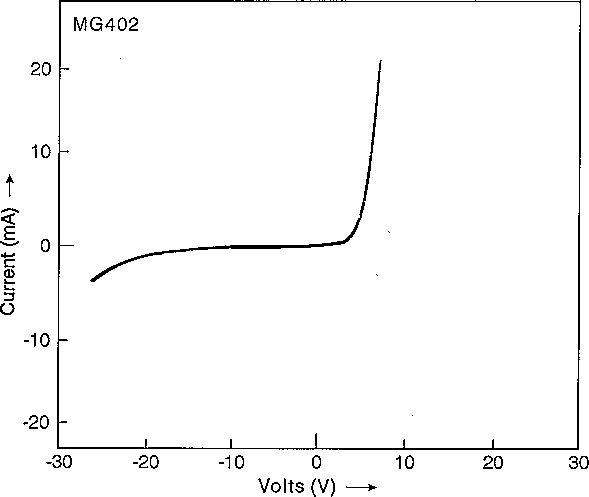
Figure 2. A typical low temperature PL spectrum for an epitaxial layer of GaN grown on (1 1 1)B substrate under optimum conditions of temperature and V:III ratio.
Under the same growth conditions we have grown p-n junction diodes on GaAs (1 1 1)B n+ substrates using Si doping for the approximately 1μm thick n-region followed by Mg doping for the p-region. The I-V spectrum for this sample is shown in see Figure 3 taken using a standard curve tracer at room temperature using contacts to the front surface and the substrate. The turn-on voltage is about 3 eV as would be expected. A reverse breakdown at −15 V is consistent with a doping level in the lightly p-doped region around 1017 cm−3. Mesa isolated and properly contacted samples are being prepared for studies of the light vs. current characteristics.
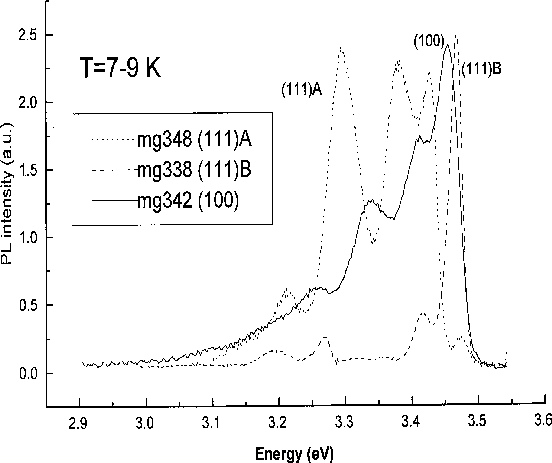
Figure 3. An I-V curve for a GaN p-n junction device grown on a Si doped (1 1 1)B GaAs substrate. Data were obtained using a front contact to the GaN film and a back contact to the GaAs.
4. Conclusions
Growth of high quality epitaxial films on (1 1 1)B oriented GaAs substrates has been demonstrated using a modified MBE method. Using this procedure it is possible to fabricate directly p-n junction diodes on n+ GaAs substrates.
Acknowledgments
The authors would like to acknowledge support for this work from an ESPRIT Long Term Research Project 20968 (LAQUANI) and from the Royal Society (GBR).


