Introduction
Very little work has been performed to understand the effect of plasma damage on p-GaN. Shul et.al. [Reference Shul, Zhang, Baca, Willison, Han, Pearton, Ren, Zolper and Lester1] reported that the sheet resistance of p-GaN increased upon exposure to Inductively Coupled Plasmas (ICP) of pure Ar. The increases were almost linearly dependent on ion energy (90% increase at −350 eV), but weakly dependent on ion flux (∼25% increase at ∼1017 ions·cm−2·s−1).
Most past work in this area has focused on n- type material. The sheet resistances of GaN [Reference Eddy and Molnar2], InGaN [Reference Pearton, Lee, MacKenzie, Abernathy and Shul3], InAlN [Reference Pearton, Lee, MacKenzie, Abernathy and Shul3] and InN [Reference Pearton, Lee, MacKenzie, Abernathy and Shul3] samples were found to increase in proportion to ion flux and ion energy in an Electron Cyclotron Resonance (ECR) Ar plasma. Ren et.al. [Reference Ren, Lothian, Pearton, Abernathy, Vartuli, MacKenzie, Wilson and Karlicek4,Reference Ren, Lothian, Chen, MacKenzie, Donovan, Vartuli, Abernathy, Lee and Pearton5] examined the effect of ECR BCl3/N2 and CH4/H2 plasmas on the electrical performance of InAlN and GaN channel field effect transistors. They found that hydrogen passivation of the Si doping in the channel may occur if H2 is a part of the plasma chemistry and that preferential loss of N2 degraded the rectifying properties of Schottky contacts deposited on plasma-exposed surface. Ping et.al. [Reference Ping, Schmitz, Adesida, Khan, Chen and Yang6,Reference Ping, Chen, Yang, Khan and Adesida7] found more degradation in GaN Schottky contacts exposed to Ar plasmas relative to SiCl4 exposure, which would be expected on the basis of the faster etch rate with the latter and hence improved damage removal. In general it is found the ion damage tends to increase the n-type doping level at the surface, most likely through preferential loss of N2, and that the bandedge photoluminescence intensity decreases through introduction of non-radiative levels [Reference Chen, Pan and Chi8-Reference Satore, Matsutani, Shirasawa, Mori, Honda, Sakaguchi, Kagana and Iga12].
Understanding the effects of plasma-induced damage in GaN has become more important as the interest in electronic devices for high temperature, high power applications has increased. One clear example is in the fabrication of GaN/AlGaN heterojunction bipolar transistors (HBTs) [Reference McCarthy, Kozodoy, DenBaars, Rodwell and Mishra13-Reference Han, Baca, Shul, Willison, Zhang, Ren, Zhang, Dang, Donovan, Cao, Cho, Jung, Abernathy, Pearton and Wilson15] or GaN bipolar junction transistors (BJTs) [Reference Yoshida and Suzuki16] where it is necessary to etch down to both a p-type base layer and an n-type subcollector layer. Energetic ion damage may result in increased surface and bulk leakage currents and changes in the electrical properties of the near-surface region through a change in Ga/N stoichiometry [Reference Shul, Zhang, Baca, Willison, Han, Pearton, Ren, Zolper and Lester1]. In other compound semiconductor systems it is often possible to remove plasma-damaged regions using slow wet chemical etching [Reference Pearton17]. In the GaN system, much less is known about the electrical effects of dry etch damage, and its subsequent removal by wet etching or annealing.
We describe the results of experiments in which p-GaN was exposed to Inductively Coupled Plasmas (ICP) of Cl2/Ar, H2 or Ar. The changes in electrical properties were measured by diode breakdown voltage.
Experimental
A schematic of the final Schottky diode structures is shown in Figure 1. Plasma exposures were performed with the contacts in place. The layer structure consisted of 1μm of undoped GaN (n-5×1016 cm−3) grown on a c-plane Al2O3 substrate, followed by 0.3µm of Mg doped (p-1017 cm−3) GaN. The samples were grown by rf plasma-assisted Molecular Beam Epitaxy [Reference Van Hove, Hickman, Klaassen, Chow and Ruden18]. Ohmic contacts were formed with Ni/Au deposited by e-beam evaporation, followed by lift-off and annealing at 750°C. The GaN surface was then exposed for 1 min to ICP Cl2/Ar, H2 or Ar plasmas in a Plasma-Therm 790 System. The 2MHz ICP source power was varied from 300-1400 W, while the 13.56 MHz rf chuck power was varied from 20-250 W. The former parameter controls ion flux incident on the sample, while the latter controls the average ion energy. Prior to deposition of 250µm diameter Ti/Pt/Au contacts through a stencil mask, the plasma exposed surfaces were either annealed under N2 in a rapid thermal annealing system, or immersed in boiling NaOH solutions to remove part of the surface. As reported previously it is possible to etch damaged GaN in a self-limiting fashion in hot alkali or acid solutions [Reference Kim, Lee, Park and Kim19-Reference Lee, Kim, Lee, Park and Kim21]. The current-voltage (I-V) characteristics of the diodes were recorded on an HP 4145A parameter analyzer.
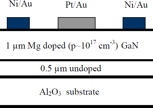
Figure 1. Schematic of completed p-GaN Schottky diode.
Results and Discussion
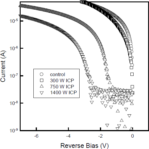
We observed an increase in reverse breakdown voltage (VB) on the p-GaN, whose magnitude was dependent on both ion energy and ion flux. The increase in breakdown voltage on the p-GaN is due to a decrease in hole concentration in the near-surface region through the creation of shallow donor states. The key question is whether there is actually conversion to an n-type surface under any of the plasma conditions. Figure 2 shows the forward turn-on characteristics of the p-GaN diodes exposed to different source power Ar discharges at low source power (300 W). The turn-on voltage remains close to that of the unexposed control sample. However there is a clear increase in the turn-on voltage at higher source powers, and in fact at ≥750 W the characteristics are those of an n-p junction [Reference Sze22]. Under these conditions the concentration of plasma-induced shallow donors exceeds the hole concentration and there is surface conversion. In other words the metal-p GaN diode has become a metal-n GaN-p GaN junction. We always find that plasma exposed GaN surfaces are N2-deficient relative to their unexposed state [Reference Shul, Zhang, Baca, Willison, Han, Pearton, Ren, Zolper and Lester1,Reference Pearton, Lee, MacKenzie, Abernathy and Shul3,Reference Ren, Lothian, Pearton, Abernathy, Vartuli, MacKenzie, Wilson and Karlicek4,Reference Ren, Lothian, Chen, MacKenzie, Donovan, Vartuli, Abernathy, Lee and Pearton5,Reference Shul, Zolper, Crawford, Hickman, Briggs, Pearton, Lee, Karlicek, Tran, Schurmann, Constantine and Barratt10], and therefore the obvious conclusion is nitrogen vacancies create shallow donor levels. This is consistent with thermal annealing experiments in which N2 loss from the surface produced increased n-type conduction [Reference Zolper, Rieger, Baca, Pearton, Lee and Stall23,Reference Brown, Ramer, Zhang, Lester, Hersee and Zolper24].

Figure 2. Forward turn-on characteristics of diodes exposed to ICP Ar discharges (150 W rf chuck power) at different ICP source powers prior to deposition of the Ti/Pt/Au contact.
The influence of rf chuck power on the diode I-V characteristics is shown in Figure 3 for both H2 and Ar discharges at fixed source power (500 W). A similar trend is observed as for the source power experiments, namely the reverse breakdown voltage increases, consistent with a reduction in p-doping level near the GaN surface.

Figure 3. I-V characteristics from samples exposed to either H2 (top) or Ar (bottom) ICP discharges (500 W source power) as a function of rf chuck power prior to deposition of the Ti/Pt/Au contact. The breakdown voltage increases with the rf chuck power employed during the plasma exposure.
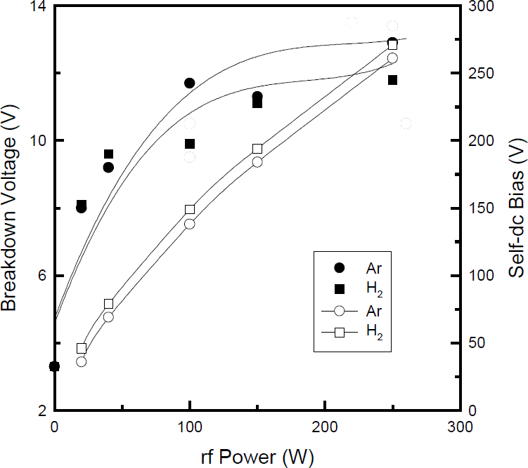
Figure 4 plots breakdown voltage and dc chuck self-bias as a function of the applied rf chuck power. The breakdown voltage initially increases rapidly with ion energy (the self bias plus ∼ 25 V plasma potential) and saturates above ∼100 W probably due to the fact that sputtering yield increases and some of the damaged region is removed. Note that there are very large changes in breakdown voltage even for low ion energies, emphasizing the need to carefully control both flux and energy. We should also point out that our experiments represent worse-case scenarios because with real etching plasma chemistries such as Cl2/Ar, the damaged region would be much shallower due to the much higher etch rate. As an example, the sputter rate of GaN in a 300 W source power, 40 W rf chuck power Ar ICP discharge in ∼40 Å·min−1, while the etch rate in a Cl2/Ar discharge under the same conditions is ∼1100Å·min−1.

Figure 4. Variation of diode breakdown voltage in samples exposed to H2 or Ar ICP discharges (500 W source power) at different rf chuck powers prior to deposition of the Ti/Pt/Au contact (solid symbols). The dc chuck self-bias during plasma exposure is also shown (open symbols).
Figure 5 shows I-V characteristics from samples that were wet etched to various depths in NaOH solutions after exposure to either Cl2/Ar or Ar discharges (500 W source power, 150 W rf chuck power, 1 min). For these plasma conditions we did not observe type conversion of the surface. However, we find that the damaged GaN can be effectively removed by immersion in hot NaOH, without the need for photo- or electrochemical assistance of the etching. The VB values increase on p-GaN after plasma exposure due to introduction of shallow donor states that reduce the net acceptor concentration.

Figure 5. I-V characteristics from p-GaN samples exposed to ICP Cl2/Ar (top) or Ar (bottom) discharges (500 W source power, 150 W rf chuck power) and wet etched in boiling NaOH to different depths prior to deposition of the rectifying contact.
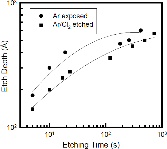
Figure 6 shows the wet etch depth in plasma damaged p-GaN as a function of etching time. The etch depth saturates at depths of 500-600Å, consistent with the electrical data. It has previously been shown by Kim et.al. [Reference Kim, Lee, Park and Kim19] that the wet etch depth on thermally- or ion-damaged GaN was self-limiting. This is most likely a result of the fact that defective or broken bonds in the material are readily attacked by the acid or base, whereas in undamaged GaN the etch rate is negligible. I-V characteristics were recorded from samples exposed to 750 W source power, 150 W rf chuck power (-160 V dc chuck bias) Ar discharges and subsequently wet etched to different depths using 0.1 M NaOH solutions before deposition of the Ti/Pt/Au contact. Figure 7 shows the effect of the amount of material removed on the diode breakdown voltage. Within the experimental error of ±12%, the initial breakdown voltage is reestablished in the range 400-450Å. This is consistent with the depth obtained from the etch rate experiments described above. These values are also consistent with the damage depths we established in n-GaN diodes exposed to similar plasma conditions [Reference Cao, Cho, Pearton, Dang, Zhang, Ren, Shul, Zhang, Ren, Shul, Zhang, Baca, Hickman and Van Hove25].

Figure 6. Wet etch depth versus etch time in boiling 0.1M NaOH solutions for plasma damaged p-GaN.

Figure 7. Variation of VB with depth of plasma exposed p-GaN removed by wet etching prior to deposition of the rectifying contact. The dashed line shows the control value in unexposed p-GaN diodes.
We also performed annealing experiments on the plasma-damaged p-GaN at temperatures up to 900°C under a N2 ambient. At this temperature the VB values were returned to within 10% of their control values. Annealing at higher temperatures degraded the electrical properties, most likely due to nitrogen loss for the surface.
Summary and Conclusions
ICP plasma exposure of p-GaN produced large increases in reverse breadown voltage, independent of the plasma chemistry employed. The results are consistent with creation of nitrogen vacancy-related shallow donors in the near-surface region (<600Å). Although not discussed here, the damage was found to accumulate in this region even for very short plasma exposure times (3-4 secs). Two different methods for restoring VB were investigated. Annealing at 900°C essentially returned VB to its original, control value, whereas wet etch removal of the damaged surface in boiling NaOH prior to deposition of the Schottky contact was also effective in restoring the initial electrical properties.
Acknowledgements
The work at UF is partially supported by a DARPA/EPRI grant, No. MDA972-98-1-0006 (D. Radack and J. Melcher) monitored by ONR (J.C. Zolper) and a NSF grant DMR97-32865 (L.D. Hess). Sandia is a multiprogram laboratory operated by Sandia Corporation, a Lockheed-Martin Company, for the US Department of Energy under contract No. DEAC04-94-AC-85000.