


Introduction
Disordered dielectric metal and semiconductor oxide thin films are of great technological importance for a wide range of electronic applications, especially in the semiconductor industry (Kingon et al., Reference Kingon, Maria and Streiffer2000; Fortunato et al., Reference Fortunato, Barquinha and Martins2012; Edwards et al., Reference Edwards, Barnaby, Campbell, Kozicki, Liu and Marinella2015; Yu et al., Reference Yu, Marks and Facchetti2016), as gate oxides in transistors (Robertson, Reference Robertson2006) or tunnel barriers in non-volatile memories (Garcia Ruiz et al., Reference Garcia Ruiz, Tienda-Luna, Godoy, Donetti and Gamiz2009). A broad understanding and careful characterization of these devices at the nanoscale is of particular importance for further technological advances (Fortunato et al., Reference Fortunato, Barquinha and Martins2012). Due to continued device miniaturization, advanced characterization tools such as high-resolution and in situ transmission electron microscopy (TEM) techniques are essential and well established to understand the structure–property correlations (Rudneva et al., Reference Rudneva, Gao, Prins, Xu, van der Zant and Zandbergen2013; Kamaladasa et al., Reference Kamaladasa, Sharma, Lai, Chen, Salvador, Bain, Skowronski and Picard2014).
Recently, new types of electrical memories have been investigated, such as memristors (Kim et al., Reference Kim, Gaba, Wheeler, Cruz-Albrecht, Hussain, Srinivasa and Lu2012a, Reference Kim, Sah, Yang, Cho and Chua2012b; Zahari et al., Reference Zahari, Hansen, Mussenbrock, Ziegler and Kohlstedt2015), to allow binary or analog switching behavior (Strukov et al., Reference Strukov, Snider, Stewart and Williams2008). Redox-based memristors typically work on the principle of valence state change, where migration of anions and vacancies result in local redox reactions creating pathways for higher conductivity (low resistive state) and vice versa for lower conductivity (high resistive state). In both cases, the matrix for cation and vacancy migration is typically a thin film oxide (Edwards et al., Reference Edwards, Barnaby, Campbell, Kozicki, Liu and Marinella2015; Ielmini, Reference Ielmini2016; Zidan et al., Reference Zidan, Chen, Indiveri and Lu2017; Wang et al., Reference Wang, Rao, Midya, Joshi, Jiang, Lin, Song, Asapu, Zhuo, Li, Wu, Xia and Yang2018). Experimentally demanding work has been conducted to understand the structure, processes and dynamics of memristive materials, and devices down to the atomic scale (Ha & Ramanathan, Reference Ha and Ramanathan2011; Yao et al., Reference Yao, Zhong, Natelson and Tour2012; Fan et al., Reference Fan, Fan, Li and Dong2013; Park et al., Reference Park, Kim, Park, Li, Heo, Lee, Chang, Kwon, Kim, Chung, Dittmann, Waser and Kim2013; Gale, Reference Gale2014; Strobel et al., Reference Strobel, Hansen, Dirkmann, Neelisetty, Ziegler, Haberfehlner, Popescu, Kothleitner, Chakravadhanula, Kübel, Kohlstedt, Mussenbrock and Kienle2017). One of the critical issues in these studies is the complex data interpretation and evaluation to understand bulk materials/device properties from the local observations. One of the challenges involves sample preparation (Mayer et al., Reference Mayer, Giannuzzi, Kamino and Michael2007; Langford & Rogers, Reference Langford and Rogers2008). For example, Ga implantation and defect generation during focused ion beam (FIB) sample preparation (Frey et al., Reference Frey, Lehrer and Ryssel2003) and contamination during Pt, W, or C deposition (Hammad Fawey et al., Reference Hammad Fawey, Chakravadhanula, Reddy, Rongeat, Scherer, Hahn, Fichtner and Kübel2016), as well as redeposition (Cairney & Munroe, Reference Cairney and Munroe2003) cannot be completely avoided. Furthermore, surface effects, e.g. due to differences in diffusion properties can play a critical role, as well as the interaction with and damage by the electron beam (Aitken et al., Reference Aitken, Young and Pan1978; Berger et al., Reference Berger, Macaulay and Brown1987; Egerton et al., Reference Egerton, Li and Malac2004) during TEM characterization, leading, for example, to the generation of oxygen deficient structures (Egerton et al., Reference Egerton, McLeod, Wang and Malac2010). While these effects are often quite well understood for ex situ analysis, in situ studies are more sensitive as the effects of these artifacts on the processes and physical properties are typically not well established. Depending on the properties of interest, small structural changes induced by the electron beam can potentially alter reaction pathways or properties of the materials/devices.
Electron beam damage is well known to be critical in in situ battery studies due to the sensitive lithium compounds (Lin et al., Reference Lin, Markus, Doeff and Xin2014; Mehdi et al., Reference Mehdi, Qian, Nasybulin, Park, Welch, Faller, Mehta, Henderson, Xu, Wang, Evans, Liu, Zhang, Mueller and Browning2015) and the organic electrolytes (Drummy et al., Reference Drummy, Yang and Martin2004), even though the detailed effects on the reaction pathways during electrochemical cycling are often not established. In case of metal oxides or semiconductor oxides, electron beam damage is typically only considered to be a significant factor for TEM analysis at very high dose. This is partially because the structural changes due to the electron beam are often difficult to identify clearly, especially in amorphous oxides. However, the electrical response can be drastic, even at fairly low dose, for both low and high voltage scanning electron microscopy (SEM) and TEM. In this paper, we attempt to identify the changes in semiconductor and metal oxide systems during electron beam irradiation and correlate them with the electrical changes. We will discuss the electron beam induced damage using SiO2, TiO2, and NbxOy as examples to study the damage mechanism, the structural changes induced and, in particular, the effect on the electrical properties. These results will be put in perspective with regard to in situ SEM/TEM measurements involving these oxides. The results of these studies can be applied to a wide range of applications, where typical oxide materials are studied and patterned by means of the electron beam—e.g. for electron beam lithographic techniques.
Methods and Materials
TEM analysis was performed using an aberration (image) corrected Titan 80-300 microscope (FEI Company, Portland, OR, USA) equipped with a US1000 slow scan CCD camera and a Tridiem 863 image filter (Gatan Inc., Pleasanton, CA, USA). The microscope was operated at 300 kV for beam damage studies. Energy filtered TEM (EFTEM) analysis was performed using a 5 eV energy slit centered on an energy loss of 17 eV to image the silicon distribution (Iacona et al., Reference Iacona, Bongiorno, Spinella, Boninelli and Priolo2004) in the silicon oxide films. The electron dose rate was calculated from unfiltered TEM images, without a sample, with 1 s exposure time, acquired using the same illumination settings and camera, utilizing the calibrated conversion rate of counts to electrons of the camera.
The real space damage analysis of SiO2 was performed using 20 nm silicon oxide windows (SO100 A20Q33A, Simpore, West Henrietta, NY, USA) as test object, applying a dose rate of 1.76 × 10⁴ e/nm2 s.
For the electron beam damage dependent conductivity measurements, a parallel electron beam illumination in TEM mode was used with a defined electron beam diameter of 36 or 16 µm. Dose rates of 670 and 1,100 e/nm2 s were applied for SiO2 and 1,100 e/nm2 s in the case of NbO2. As TiO2 is more sensitive to the beam, it was exposed to a lower dose rate of 45 e/nm2 s. The oxide thin films were directly deposited on MEMS-based electrical devices for the in situ measurements (E-AEK11, Protochips Inc., Morrisville, NC, USA) using various deposition methods:
(1) ~15 nm silicon oxide was deposited by plasma enhanced chemical vapor deposition (PECVD) (Hartel et al., Reference Hartel, Hiller, Gutsch, Löper, Estradé, Peiró, Garrido and Zacharias2011),
(2) ~15 nm silicon oxide was deposited by DC reactive magnetron sputtering (Supporting data—Experimental),
(3) ~30 nm titanium oxide was deposited by pulsed laser deposition, and
(4) ~30 nm niobium oxide was deposited by magnetron sputtering (Strobel et al., Reference Strobel, Hansen, Dirkmann, Neelisetty, Ziegler, Haberfehlner, Popescu, Kothleitner, Chakravadhanula, Kübel, Kohlstedt, Mussenbrock and Kienle2017). The stoichiometry of the films was determined by X-ray photoelectron spectroscopy (XPS) (Supporting information—XPS results).
A FUSION 200 electrical holder (Protochips Inc., Morrisville, NC, USA) with a Keithley 2636A SourceMeter (Tektronix Inc., Beaverton, OR, USA) and a Reference 600 potentiostat (Gamry Instruments, Warminster, PA, USA) was used for electrical measurements. A schematic of the chip and the electron beam exposed area is shown in Figure 2e. Voltage controlled I/V cycles were acquired over ±3 V with a scan speed of 66 mV/s. The electron beam was always turned off during the measurement to prevent the electron beam current contributing to the I/V curve (as an exception, the graphs in Supplementary Fig. S7 show the electron beam effect on the I/V measurement for TiO2 and NbxOy). In the case of silicon oxide, the first I/V curve was neglected as charging effects of the sample contribute to the first I/V curve. The second and third I/V curves are quite similar suggesting that all electron beam induced charging has been removed. The I/V curves and values shown in this paper for silicon oxide are always from the third I/V curve.
Low-voltage measurements were performed in a SEM using an Auriga 60 (Carl Zeiss AG, Oberkochen, Germany) dual beam FIB. A Faraday cup was used to measure the electron beam current at different operation voltages between 2 and 30 kV for various spot sizes to determine the dose rate and total dose. The conductivity measurements were performed using the same samples as previously in the TEM.
Results and Discussion
Electron Beam Irradiation of Silicon Oxide
The electron beam induced damage in silicon oxide is interesting because it is one of the most established oxides for microelectronic applications. Similar to previous work (Gutsch et al., Reference Gutsch, Hiller, Laube, Zacharias and Kübel2015), EFTEM dose series, acquired on pure SiO2 thin films (TEMwindows, West Henrietta, NY, USA) at an energy loss of 17 eV, reveal the continuous formation of silicon-rich mostly disordered particles with increasing dose (Fig. 1) due to an electron beam induced reduction of the silicon oxide film. Initially, at 300 kV and a dose of up to 1.9 × 10⁶ e/nm2 with a dose rate of ~1.76 × 10⁴ e/nm2 s no silicon nanoparticles are visible in the EFTEM images of the film, only a slight cloudy appearance can be noticed. With increasing dose, particles start to segregate visibly, and both the number and average size of these particles increase with dose. Hence, the distance between the particles is reduced considerably, forming a close (perhaps interconnected) network of particles at a dose of ~8.5 × 10⁶ e/nm2. A further increase in dose eventually led to film degradation, to formation of holes, and finally breakage of the film. This is illustrated in Figure 1 for operation at 300 kV; similar damage was also observed at 80 kV (Gutsch et al., Reference Gutsch, Hiller, Laube, Zacharias and Kübel2015). In order to understand the electron beam induced structural changes in silicon oxide, radial distribution functions (RDFs) by selected area electron diffraction (SAED) are recorded. The short-range order of the pristine amorphous SiO2 thin film indicates that the as-prepared amorphous sample is similar to the structure in quartz. A distinctive peak in line with the Si–Si bond length in Si–diamond appears after dose of 3.7 × 10⁷ e/nm2. In addition, the reduced peak intensities corresponding to the Si–O and O–O distances compared to the pristine state shows that the sample is oxygen deficient. These observations indicate the reduction of the SiO2 phase and an increase of the Si phase in the exposed area. In agreement with the EFTEM analysis, this confirms that the bright particles are a Si-rich phase with direct Si–Si bonding.
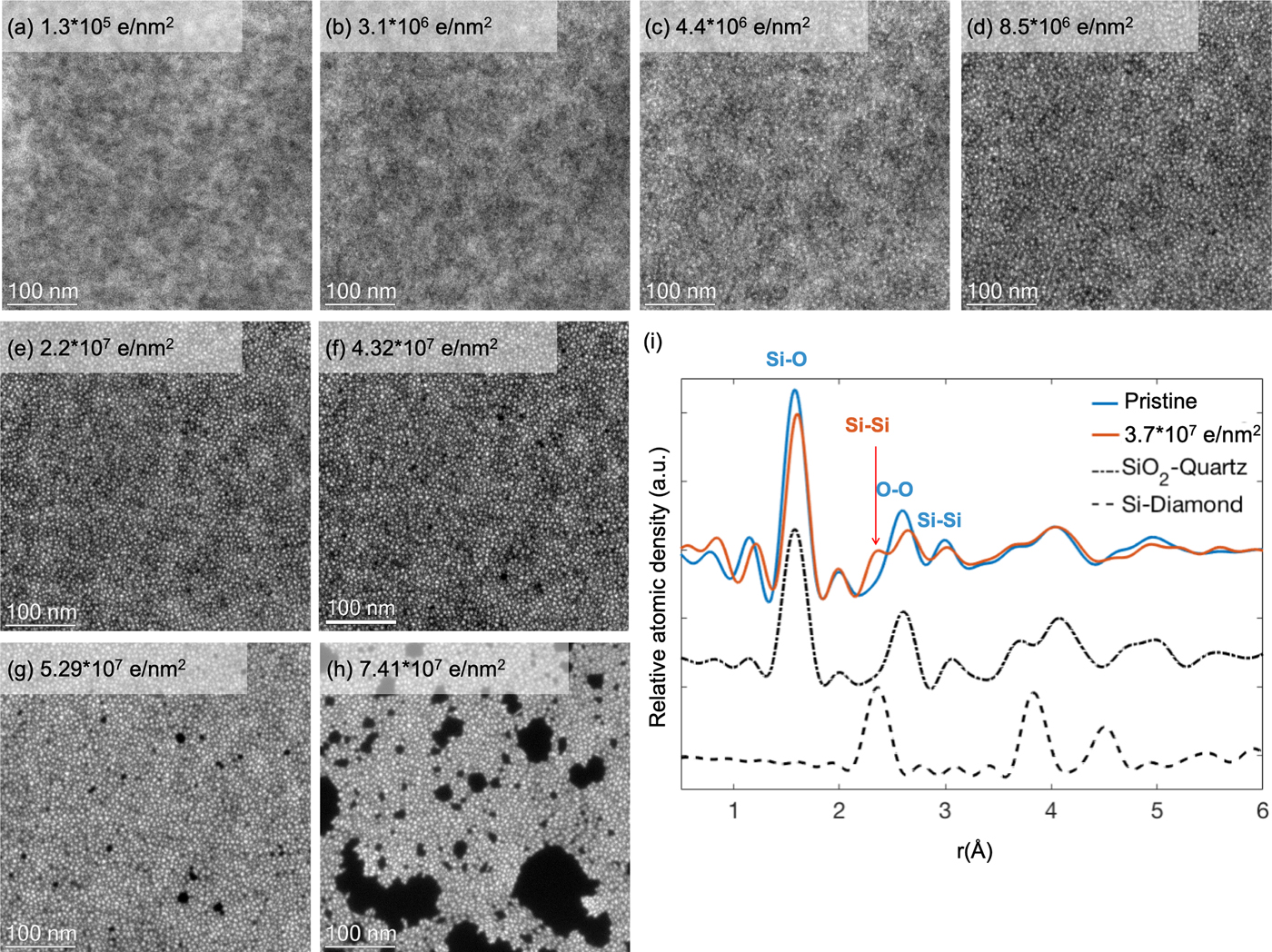
Fig. 1. EFTEM (at 17 eV energy loss) dose series showing Si nanoparticle formation under the electron beam. The dose rate was ~1.76 × 10⁴ e/nm2 s; the total dose is shown as inset in the images (a–h). (i) RDF analysis of the pristine silicon oxide film (blue curve) and beam induced damaged film after a dose of 3.7 × 10⁷ e/nm2 (red curve) with calculated RDFs (black) for crystalline SiO2–quartz (dot dash curve) and crystalline Si–diamond (dash curve).
Insulator to Semiconductor Transition
The silicon nanoparticles produced by the electron beam irradiation within the oxide (Fig. 1) resemble the silicon nanoparticle arrays investigated as active layer for silicon-based LEDs (Zacharias et al., Reference Zacharias, Heitmann, Scholz, Kahler, Schmidt and Bläsing2002; Heitmann et al., Reference Heitmann, Schmidt, Zacharias, Timoshenko, Lisachenko and Kashkarov2003). The conductivity of the material would be expected to increase, when a dense non-connected network has formed enabling electrical transport by tunneling between particles and increase further when an interconnected network is formed by electron beam reduction.
We investigated the electrical properties of the electron beam irradiated silicon oxides by measuring in situ dose dependent I/V curves as described in the experimental section for PECVD deposited SiO2 thin films. Figures 2a to 2d show the effect of the electron beam and the structural changes induced on the conductivity of the silicon oxide film. Initially (Fig. 2a), the I/V curve displays the typical shape of a capacitor, thus indicating that the as-prepared SiO2 thin film behaves as an insulator. After electron beam exposure with a total dose of ~3 × 10⁷ e/nm2, the I/V curve (Fig. 2b) shows a significant increase in conductivity. This change in conductivity is related to the electron beam induced reduction of the film (charging effects due to the electron beam have been excluded). Considering the dose, we assume that the change in conductivity is related to the formation of a dense or even fully connected network of silicon particles within the oxide film. The resulting Si nanoparticle network significantly increases the electron mobility in the film. Due to the absence of dopants in the material, charge carriers have to be injected into the film from the contacts. Therefore, the conductivity is limited by the resulting space-charge that opposes the applied electric field.
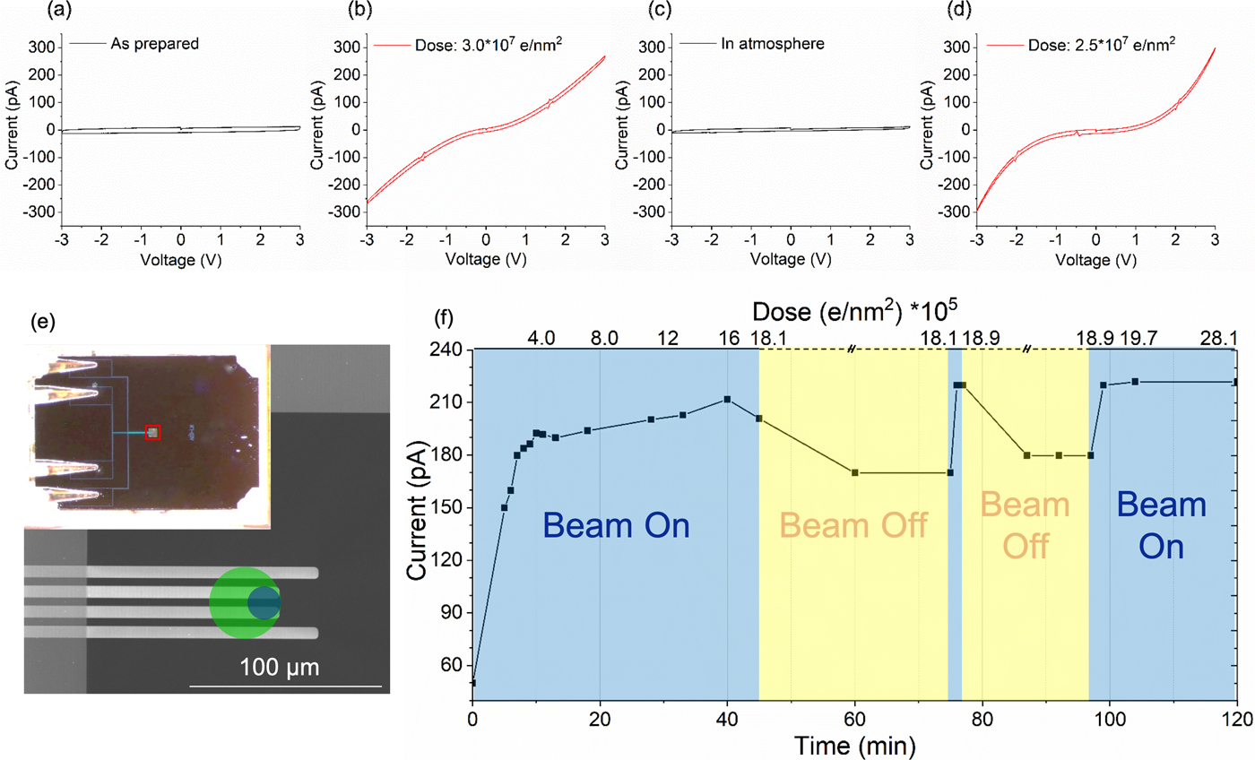
Fig. 2. I/V measurement on PECVD deposited SiO2: transformation from insulating (a) to conductive (b) after electron beam exposure (dose ~3 × 10⁷ e/nm2), back to insulator (c) after exposure to atmosphere and finally back to conductive (d) after further electron beam exposure (dose 2.5 × 10⁷ e/nm2). Dose rate: ~670 e/nm2 s. e: Schematic of the electrical chip. The green circle shows the area (D = 36 µm) exposed by the electron beam for SiO2 and the blue circle (D = 16 µm) for titanium and niobium oxides for conductivity measurements. f: Electron beam induced conductivity changes and oxygen sensitivity of PECVD deposited SiO2: current measured at 3 V depending on dose and reoxidation time in the TEM.
The insulator to semiconductor behavior is reversible. When the sample is exposed to air, the electrical characteristics change back to a capacitive behavior (Fig. 2c). We assume that such reversibility is based on a partial re-oxidation of the silicon particles/network within the thin film in air causing a deterioration of the connected network and hence a low conductivity of the film. Subsequent electron beam exposure switches the behavior back to a semiconducting state (Fig. 2d). This switching between capacitive and conductive behavior by exposure to the electron beam and air can be repeated extensively for both the PECVD and the magnetron sputtered silicon oxide films (data not shown). Interestingly, during the second (or further) electron beam exposure, a much lower dose is sufficient to achieve the switching compared to the first cycle. We tried to image the differences between the exposed and reoxidized state by EFTEM (Fig. S4). However, imaging the broken network turned out to be difficult, as the dose for the second electron beam reduction is much less than the minimum dose required to record an EFTEM image at sufficient resolution and signal to noise to detect the particles (see critical dose for conductivity changes of a pre-irradiated sample later).
Electron Dose Dependence
The evolution from insulator to semiconductor was examined in more detail for the magnetron sputtered SiO2 thin film (Fig. 3a). Initially, the film was insulating, resulting in a capacitive element in our setup prior the electron beam exposure (black I/V curve). With increasing dose, the evolution from a capacitive to a semi-conductive behavior can be seen clearly. The corresponding evolution of the maximum current at 3 V is plotted in Figure 3b. The plot clearly shows that during the early stages of electron beam exposure, up to a dose of ~4.8 × 10⁷ e/nm2, essentially no conductivity change is observed. Afterward, first a slight increase in the conductivity, and then at 6.3 × 10⁷ e/nm2, a significant increase is observed. This general behavior would fit the silicon particle evolution presented before: during an incubation time, no significant conductivity change is observed until the silicon particle network is dense enough to enable charge transport by tunneling. Once an interpenetrating network is formed, the conductivity should increase significantly again.
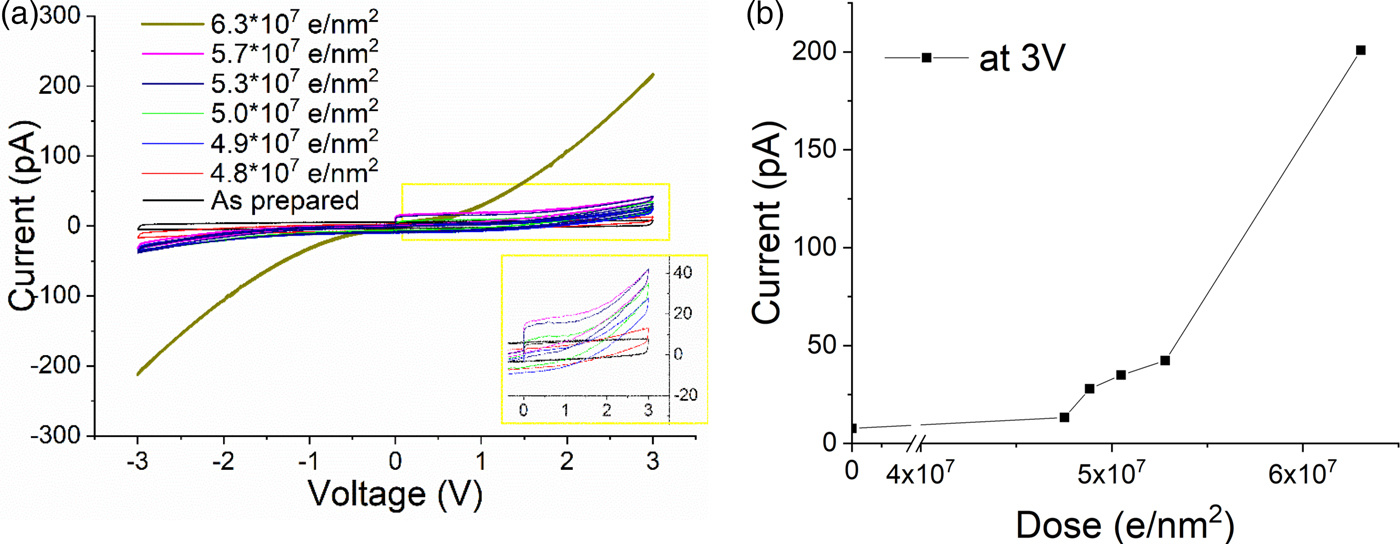
Fig. 3. a: I/V cycles showing the evolution of a magnetron sputtered SiO2 from capacitive to a conductive state. Dose rate 1,100 e/nm2 s. b: Electron beam (300 kV) induced conductivity changes: dose versus current at 3 V.
The absolute dose measured for the increase in conductivity roughly fits the dose needed for significant nanoparticle formation as imaged by EFTEM (cf. Fig. 1g). However, the exact numbers do not match perfectly. This might be partially due to slight differences between the films (thickness, free standing versus SiN-supported, deposition conditions). However, probably more significant are dose rate and the experimental time during the study: as discussed in the beginning, reoxidation of the films leads to a recovery of the capacitive behavior. This reoxidation also occurs within the vacuum system of the TEM, due to the residual oxygen pressure in the TEM column and results in competing reduction and oxidation effects causing strong dose rate sensitivity. Unfortunately, it was experimentally not possible to use comparable dose rates for EFTEM imaging (1.76 × 10⁴ e/nm2 s) and the conductivity measurements (6.7 × 10² e/nm2 s) because of the different illuminated areas for both measurements.
Reoxidation within the TEM column was investigated using one of the PECVD grown SiO2 thin films. Figure 2f shows the evolution of the maximum current at 3 V with respect to time and dose during the third electron irradiation cycle (the corresponding I/V plots are shown in Supplementary Fig. S5). The initial conductivity is a bit higher than in the as-prepared state, suggesting that the film had not fully recovered from the previous electron beam exposure prior to this experiment. After the third electron beam exposure was started, the maximum current quickly increased and asymptotically approached a maximum value of ~210 pA after around 40 min of exposure at a dose rate of 670 e/nm2 s. When the electron beam was turned off for 30 min, the maximum current decreased by ~20%. A brief exposure to the electron beam results in a recovery of the maximum current and when the beam was turned off again, a decrease in the conductivity was observed again. This suggests that the network is more or less fully formed after 40 min during the third cycle and reoxidation without the electron beam leads to the observed reduction of the conductivity, just much slower compared to exposure to air.
An important point is that already after 5 min beam exposure, corresponding to a dose of 2 × 10⁵ e/nm2, the current increased by 100 pA compared to the starting point of the third cycle. This dose is significantly lower compared to the 3 × 10⁷ e/nm2 required to initially observe an increased conductivity during the first cycle of this experiment (Figs. 2a–2d). This large difference of the dose required during initial and later electron beam illumination is because the sample does not reoxidize completely, but just enough to destroy the interconnected silicon network. Therefore, already a low dose is causing sufficient reduction during the following illumination to recreate the silicon network.
Supplementary Figure S6a shows further details on the recovery of the capacitive state in atmosphere, illustrating the evolution of the maximum current with time in air. As soon as the sample is in air the maximum current at 3 V immediately drops from ~250 to 100 pA and slowly reduces further to a saturation condition after about 3 h. It does not reach the as-prepared condition (maximum current ~15 pA—capacitive state), even after 10 h, indicating some residual leakage current in the film due to incomplete reoxidation.
Figure 4 schematically shows the electron beam induced evolution of the SiO2 thin film into a composite with silicon particles embedded and its recovery as deduced from the EFTEM imaging and the conductivity measurements. The electron beam irradiation of the SiO2 thin film causes formation of silicon-rich nanoparticles in the irradiated area. Increasing dose increases the particle size and the density of particles drastically, thus reducing the distance between them. In turn, the connected particles change the electrical properties of the film from a capacitive to a semiconducting state. When the film is exposed to air, the surface of these particles is reoxidized, increasing their distance and thus destroying an interconnected silicon network. This transforms the material from a semiconductor back to an insulator. When the sample is exposed to the electron beam again, even at low dose, we observe a rapid change in the conductivity of the film.
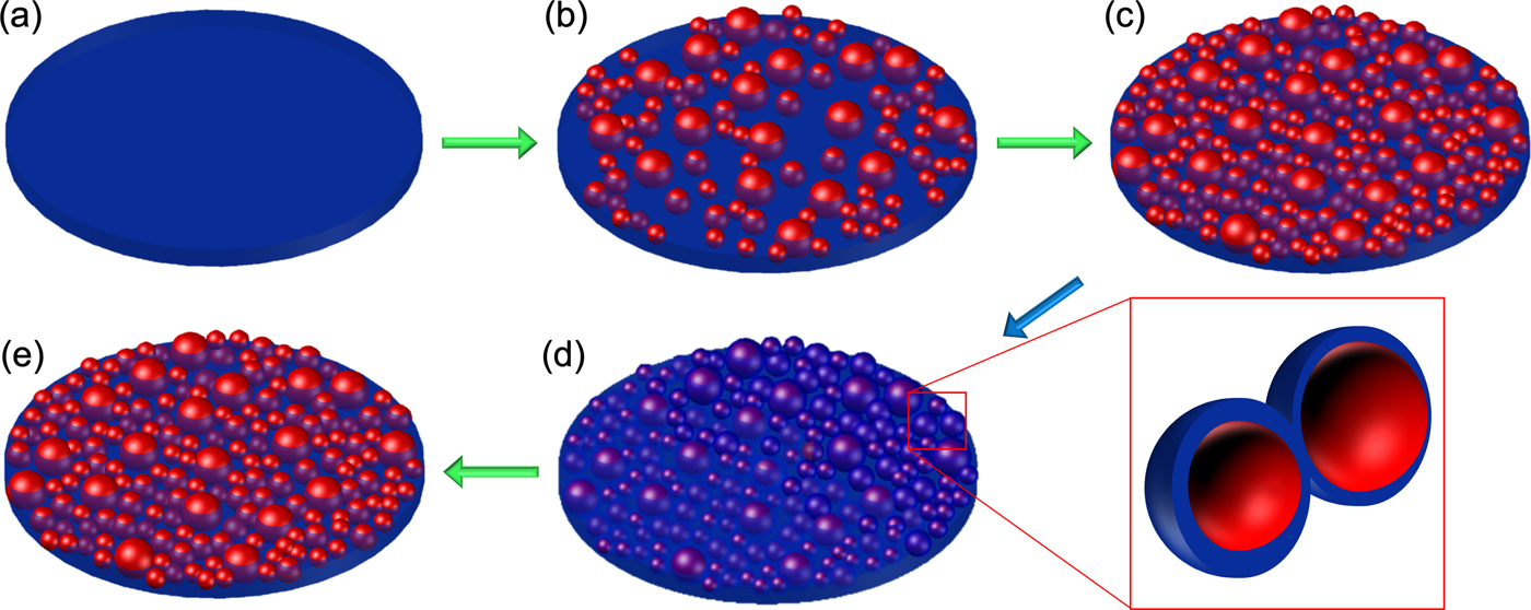
Fig. 4. Schematic illustration of the electron beam induced damage of the silicon oxide thin film leading to silicon particle formation in a composite with increasing dose (green arrow) (a–c) and resulting in an increased conductivity of the thin film. Once the sample is in atmosphere (blue arrow), a thin oxide layer forms on their surface (d) leading to the particles being disconnected from the network. Further exposure to the electron beam forms a connected network again (e) increasing the conductivity of the sample.
This observed effect of the electron beam on the electrical properties of silicon oxide might also be related to an earlier work by Mačković et al., where a change from brittle fracture to ductile was reported in silicon oxide nanospheres (Mačković et al., Reference Mačković, Niekiel, Wondraczek, Bitzek and Spiecker2016) and thin films (Mačković et al., Reference Mačković, Przybilla, Dieker, Herre, Romeis, Stara, Schrenker, Peukert and Spiecker2017).
Comparing the electron beam sensitivity observed in our electrical measurements on SiO2 (~5 × 10⁷ e/nm2), and the changes observed in EFTEM (~2 × 10⁶ e/nm2), with the electron beam sensitivity of organic materials such as pentacene or Cu-phthalocyanine (~104–5 × 10⁴ e/nm2) (Drummy et al., Reference Drummy, Yang and Martin2004), which are well known to be highly beam sensitive, the beam sensitivity at 300 kV is approaching that of small aromatic molecules and polymers.
The nucleation of Si nanoparticles in SiO2 films irradiated by UV or soft-X-ray radiation has been reported to proceed via conversion of SiO2 to SiOx and oxygen desorption followed by disproportionation of SiOx to Si and SiO2 at elevated temperatures (Akazava, Reference Akazava2001), which could be compared to the mechanism for the electron beam induced formation and growth of silicon nanoparticles. Kumar et al. reported the densification of silica in SiO2/HfO2 multi-layers during neutron irradiation, which might be related to silicon particle formation, as well as void formation in SiO2/Al2O3 multi-layers together with neutron induced silicon and aluminum diffusion within the multi-layers (Kiran Kumar et al., Reference Kiran Kumar, Leonard, Jellison and Snead2015). Changes of the electrical properties of quartz films due to heavy ion irradiation have been reported by Bush et al. and are discussed in terms of midgap interface states related to different trivalent silicon centers (Busch et al., Reference Busch, Slaoui, Siffert, Dooryhee and Toulemonde1992). MD simulations suggest the formation of more extensive structural damage leading to modification of the Si–O network and the formation of Si tetrahedra due to irradiation (Wang et al., Reference Wang, Yu, Pignatelli, Sant and Bauchy2015). While a direct comparison of these results with the damage in the amorphous silica thin films is not possible, the strong conductivity changes observed in our films are not related to individual defect centers as they only occur at a dose where a significant silicon nanoparticle density has been reached.
Electron Beam Damage of Titanium Oxide
Not only are silicon oxides sensitive to electron beam irradiation, but also metallic oxides. For example, for TiOx Berger et al. have shown that the material changes at high current densities (Berger et al., Reference Berger, Macaulay and Brown1987). Therefore, we used amorphous TiO2 as another candidate to evaluate the electron beam sensitivity and its effect on the electrical properties. As it turned out, the electrical properties of TiO2 are extremely beam sensitive even at very low dose. The I/V plots in Figure 5 show an insulating behavior of the TiO2 thin film before exposure to the electron beam. At a dose of ~2.0 × 10⁵ e/nm2 and a dose rate of 670 e/nm2 s, we could identify the formation of a metallic material with the measured current being ~1,000 times higher compared to the irradiated semiconductor silicon oxide film. Similar to the silicon oxide case, the electron beam induced reduction is reversible upon reoxidation. This occurs instantaneously in air or slowly in the TEM because of the low oxygen partial pressure.
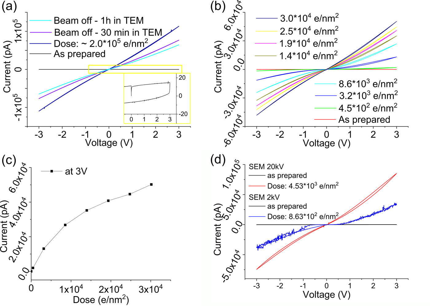
Fig. 5. I/V curves recorded after electron beam exposure of titanium oxide thin films: (a) as-prepared film and after exposure to a total dose of 2.0 × 10⁵ e/nm2 resulting in a metallic conductivity; electron dose rate: 670 e/nm2 s. After 30 and 60 min of the sample inside the TEM column (beam off), the conductivity is reduced considerably due to reoxidation; (b) I/V curves showing the evolution from a capacitive to a conductive state with increasing dose at a dose rate of 45 e/nm2 s. c: Electron beam induced conductivity changes plotted as electron dose versus max. current at 3 V [from (b)]. d: I/V cycles showing the electron beam induced damage in a SEM of titanium oxide: as-prepared and after electron beam exposure at 20 kV—dose rate of 151 e/nm2 s and at 2 kV—dose rate of 0.62 e/nm2 s.
The electron beam induced evolution of the conductivity was studied in more detail using a low current density of 45 e/nm2 s. Figure 5b shows the continuous increase in conductivity of the film with increasing dose. The first conductivity increase was detectable immediately after 10 s exposure at a dose as low as 4.5 × 10² e/nm2. Thus, the electrical response of amorphous TiO2 is around a factor of 1,000 more sensitive to the electron beam compared to SiO2. The material generated at low dose shows an I/V curve characteristic of a semiconductor. Only at a higher dose of 3.0 × 10⁴ e/nm2, we see a transition to a metallic conductor.
Presumably, the transition from an insulator to a semiconductor and then to a metallic material upon electron beam exposure is related to reduction leading to the formation of TiO2−x due to the progressive formation of oxygen vacancies. This electron beam reduction induced conductivity change is in line with the electrical properties of titanium suboxides reported by Bartholomew & Frankl (Reference Bartholomew and Frankl1969). The reason for the conductivity change being detected already at very low dose can be understood by the high sensitivity of the electrical conductivity on the oxygen content of TiO2−x (Bartholomew & Frankl, Reference Bartholomew and Frankl1969; Xu et al., Reference Xu, Sohn, Mohassab and Lan2016), with, for example, the magneli phases Ti3O5, Ti4O7, Ti5O9, and Ti6O11 being reported as highly conductive. The conductivity difference of TiO2 and Ti4O7 has also been discussed by Kwon et al. and these may be the active phases involved in switching states in TiO2-based memristors (Kwon et al., Reference Kwon, Kim, Jang, Jeon, Lee, Kim, Li, Park, Lee, Han, Kim and Hwang2010). Thus, the electrical response is different from the case of SiO2 reduction, where first silicon-rich particles form and create an interconnected network, whereas in TiO2 the reduction induced by creation of oxygen deficiencies is responsible for the electrical changes.
The RDF analysis of the amorphous TiO2 thin film (Fig. S9) indicates that the short-range order of the pristine amorphous TiO2 thin film reflects a mixture of rutile and anatase. However, we cannot differentiate between this anatase + rutile mixture and the sub-oxide phases as their short-range order is too similar. Therefore, we cannot unambiguously evaluate the structural changes during electron beam illumination.
In order to differentiate between ionization and knock-on damage as the main degradation mechanism in the titanium oxide thin films, we measured the electron beam induced conductivity dependence on the operation voltage. Figure 5d shows I/V curves recorded for the same titanium oxide samples as previously analyzed in the TEM, after electron beam irradiation in the SEM.
Beam damage of TiO2 is also observed in the SEM at 20 kV with a dose rate of ~150 e/nm2 s and at 2 kV with a dose rate of 0.6 e/nm2 s. The transformation from an insulating state to a conductor is evident in the SEM similar to that seen in the TEM. This clearly confirms electron beam damage of the films at very low dose and very low voltage.
At 2 kV acceleration voltage, knock-on damage should not be a significant contribution, suggesting that ionization damage is critically contributing at this voltage. A true quantitative comparison of the damage is difficult because of the changing imaging conditions, dose rate and illuminated oxide area (about 2× larger in SEM compared to TEM). However, the measured current per dose and contact area is of the same order at 2, 20, and 300 kV, reduced by a factor of ~2–5 at 300 kV. If ionization was solely responsible for the damage at 300 kV, a stronger increase in electron beam stability should be observed between 20 and 300 kV (Egerton, Reference Egerton2012), indicating that at 300 kV, knock-on damage is also contributing to the damage of the sample. The influence of the electron beam on the electrical property measurements of TiO2 is similar to imaging structural changes in typical aliphatic molecules and polymers, orders of magnitude more sensitive than e.g. graphene.
Niobium Oxide
NbxOy is an insulating material in the as-prepared state, but also shows a conducting behavior after illumination with the electron beam. The dose required for the reduction is between that of SiO2 and TiO2. At a dose rate of 1,100 e/nm2 s at 300 kV, the thin film was insulating up to a dose of 1 × 10⁶ e/nm2. Thereafter, niobium oxide showed a steady increase in conductivity (Fig. 6a). However, in contrast to titanium oxide, the I/V curves indicate metallic conductivity. No transition through a semiconducting behavior has been observed. Metallic conductivity has been reported for niobium suboxides (Bach, Reference Bach2009). Similar to titanium oxide, niobium oxide seems to show a conductivity change by reduction to suboxides rather than reduction to particles as in silicon.
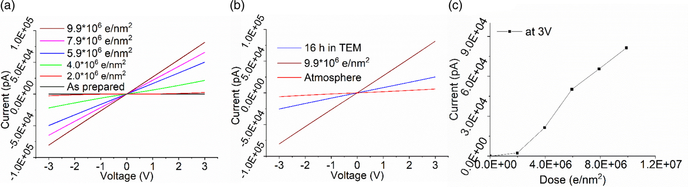
Fig. 6. I/V curves of electron beam exposed niobium oxide. Dose rate 1,100 e/nm2 s. a: Evolution of conductivity with increasing dose; (b) reoxidation leading to a slow reduction in conductivity without the beam in the TEM and fast after exposure to air; and (c) electron beam induced conductivity changes plotted as electron dose versus max. current at 3 V [from (a)].
When the sample is kept in the high vacuum of the TEM column, reoxidation leading to a reduction of conductivity (Fig. 6b) is slower compared to the titanium oxide or silicon oxide films. Only in atmosphere, the conductivity of the film drops quickly returning to the insulating material.
Comparison of the Oxide Behavior
From the dose versus resistivity plots (Fig. S10) we define a critical dose in analogy to the use of electron diffraction data for beam sensitivity analysis to compare the three oxides. For a comparison of our results to the available electron beam sensitivity data from Egerton (Reference Egerton2012), Drummy et al. (Reference Drummy, Yang and Martin2004), Wang et al. (Reference Wang, Botton, West and Hitchcock2009), and Meyer et al. (Reference Meyer, Kisielowski, Erin, Rossell and Crommie2008), Figure 7 shows the critical dose versus operating voltage for various materials. The black points represent the electron diffraction-based data from the literature. The blue points are the results obtained from the present electron beam induced conductivity studies. The green point in the plot corresponds to the first particles visible in the silicon oxide thin films by EFTEM imaging. While it is not possible to directly correlate diffraction and resistivity-based beam sensitivity measurements, it provides a basis to estimate when critical property changes are occurring in the material. The actual numbers will depend on how much structural change is needed to observe any conductivity changes. In SiO2 very significant structural changes have to occur before the resistivity changes, which is reflected by the first silicon-rich particles appearing a long time before any resistivity changes can be measured. On the other hand, in titanium (and presumably in niobium) oxide already very small structural changes are sufficient to introduce very significant resistivity changes, making the electrical measurements a very powerful tool to estimate damage. Overall, the critical dose we observe in these measurements are in the same range as for typical organic materials, indicating how crucial it is to consider electron beam effects during in situ TEM.
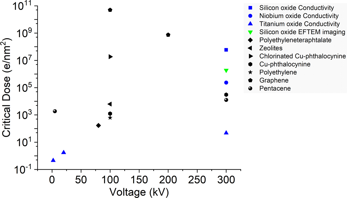
Fig. 7. Critical dose versus operating voltage for various materials (black) (Drummy et al., Reference Drummy, Yang and Martin2004; Meyer et al., Reference Meyer, Kisielowski, Erin, Rossell and Crommie2008; Wang et al., Reference Wang, Botton, West and Hitchcock2009; Egerton, Reference Egerton2012) and the present results (colored).
Conclusions
In this work, we show that even small amounts of structural damage caused by electron beam induced reduction at low dose can significantly alter the properties of amorphous oxide materials. Contrary to common experience, all three oxide films investigated in this work are prone to electron beam damage even at low doses, similar to organic materials.
Due to electron beam induced reduction, the electrical properties of SiO2, TiO2, and Nb2O5 thin films change from an insulating to a semiconducting or metallic state. The reversibility of the electron beam induced electrical properties by exposure to air is a strong indication that the damage mechanism is electron beam induced reduction of the oxides.
In SiO2 the damage proceeds via formation of silicon-rich nanoparticles in the oxide matrix, which might interconnect to a penetrating network resulting in a conductivity change. In contrast, in TiO2 and Nb2O5 the conductivity changes are directly related to the formation of suboxides, which are highly conductive. This is why the dose required for the conductivity change in silicon oxide is higher compared to the other two metal oxides. Based on the high electron beam sensitivity of TiO2 at low voltages and a slightly reduced sensitivity at 300 kV, we assume that ionization damage is the most critical contribution, but knock-on damage might also add to the reduction at high voltages. As one approach to quantify this, we defined a critical dose for electron beam damage by looking at the resistivity changes of three oxides.
We speculate that these results can be extended to other oxide materials, which will also exhibit strong beam sensitivity and corresponding changes of the electrical properties. While the effects are not drastic for most classical ex situ SEM/TEM analysis, the conductivity changes have to be critically considered for any in situ SEM and TEM measurements. These experimental results prove that electron beam effects will significantly alter in situ electrical tests.
Supplementary material
The supplementary material for this article can be found at https://doi.org/10.1017/S1431927619000175
Author ORCIDs
Christian Kübel, 0000-0001-5701-4006
Acknowledgments
This work was financially supported by Deutsche Forschungsgemeinschaft under project Forschergruppe 2093 “Memristive elements for neural systems”. X.M thanks the Deutsche Forschungsgemeinschaft (DFG) for funding of grant MU 4276/1-1. The authors gratefully acknowledge Julian Strobel, Franz Faupel, Rainer Adelung, Jürgen Carstensen, and Hermann Kohlstedt for fruitful discussions as well as Finn Niklas Zahari for Niobium oxide films used for XPS analysis and Leonardo Velasco Estrada for support in the XPS measurements of the titanium oxide films. The authors acknowledge the support of Karlsruhe Nano Micro Facility (KNMF) for the usage of the pulsed laser deposition system.


 Open access