Hostname: page-component-848d4c4894-nmvwc Total loading time: 0 Render date: 2024-06-14T22:25:30.716Z Has data issue: false hasContentIssue false

Effect of p-GaN layer on the properties of InGaN/GaN green light-emitting diodes

Published online by Cambridge University Press:  13 February 2015

Wenliang Wang
Affiliation:
State Key Laboratory of Luminescent Materials and Devices, South China University of Technology, Guangzhou 510640, China
Zuolian Liu
Affiliation:
State Key Laboratory of Luminescent Materials and Devices, South China University of Technology, Guangzhou 510640, China
Shizhong Zhou
Affiliation:
State Key Laboratory of Luminescent Materials and Devices, South China University of Technology, Guangzhou 510640, China
Weijia Yang
Affiliation:
State Key Laboratory of Luminescent Materials and Devices, South China University of Technology, Guangzhou 510640, China
Yunhao Lin
Affiliation:
State Key Laboratory of Luminescent Materials and Devices, South China University of Technology, Guangzhou 510640, China
Haiyan Wang
Affiliation:
State Key Laboratory of Luminescent Materials and Devices, South China University of Technology, Guangzhou 510640, China
Zhiting Lin
Affiliation:
State Key Laboratory of Luminescent Materials and Devices, South China University of Technology, Guangzhou 510640, China
Huirong Qian
Affiliation:
State Key Laboratory of Luminescent Materials and Devices, South China University of Technology, Guangzhou 510640, China
Guoqiang Li*
Affiliation:
State Key Laboratory of Luminescent Materials and Devices, South China University of Technology, Guangzhou 510640, China; and Department of Electronic Materials, School of Materials Science and Engineering, South China University of Technology, Guangzhou 510640, China
*
a)Address all correspondence to this author. e-mail: msgli@scut.edu.cn
Get access

Abstract

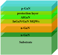
InGaN/GaN green light-emitting diodes (LEDs) have been prepared by metal-organic chemical vapor deposition with various growth temperatures for p-GaN layer. The structural and optoelectronic properties of as-grown multiple quantum wells (MQWs) and LEDs are studied in detail. It reveals that with the growth of p-GaN layer, the crystalline qualities of the as-grown n-GaN layer are improved significantly, while the optoelectronic properties of MQWs are decreased dramatically. Furthermore, the mechanisms for the effect of p-GaN growth temperature on the properties of InGaN/GaN green LEDs are proposed. It is demonstrated that the p-GaN layer grown at a suitable temperature of 950 °C shows the highest optoelectronic properties due to the fact that this suitable temperature for p-layer growth is good for the Mg doping and would not cause the fluctuation of indium in the MQWs, and eventually benefits to the effective recombination of carriers. This work provides an optimized p-GaN layer growth temperature for realizing highly efficient InGaN/GaN green LED devices.

Type
Articles
Copyright
Copyright © Materials Research Society 2015 

Access options

Get access to the full version of this content by using one of the access options below. (Log in options will check for institutional or personal access. Content may require purchase if you do not have access.)

References

REFERENCES

Kuen, L.K., Fong, W.K.P., Chan, P.K.L., and Surya, C.: Degradation mechanism of GaN-based LEDs with different growth parameters. MRS Proc. 1195, 207 (2010).Google Scholar
Gao, F.L., Guan, Y.F., Li, J.L., Gao, J.N., Guo, J.Q., and Li, G.Q.: Epitaxial growth and interfaces of high-quality InN films grown on nitrided sapphire substrates. J. Mater. Res. 28, 1239 (2013).CrossRefGoogle Scholar
Yang, W.J., Wang, W.L., Lin, Y.H., Liu, Z.L., Zhou, S.Z., Qian, H.R., Gao, F.L., Zhang, S.Z., and Li, G.Q.: Deposition of nonpolar m-plane InGaN/GaN multiple quantum wells on LiGaO2(100) substrates. J. Mater. Chem. C 2, 801 (2014).Google Scholar
Wang, W.L., Liu, Z.L., Yang, W.J., Lin, Y.H., Zhou, S.Z., Qian, H.R., and Li, G.Q.: Achieve high-quality InGaN/GaN multiple quantum wells on La0.3Sr1.7AlTaO6 substrates. Mater. Lett. 128, 27 (2014).Google Scholar
Jia, C.Y., Yu, T.J., Lu, H.M., Zhong, C.T., Sun, Y.J., Tong, Y.Z., and Zhang, G.Y.: Performance improvement of GaN-based LEDs with step stage InGaN/GaN strain relief layers in GaN-based blue LEDs. Opt. Express 21(7), 8444 (2013).Google Scholar
Zhang, L., Shao, Y.L., Hao, X.P., Wu, Y.Z., Zhang, H.D., Qu, S., Chen, X.F., and Xu, X.G.: Improvement of crystal quality HVPE grown GaN on an H3PO4 etched template. CrystEngComm 13, 5001 (2011).CrossRefGoogle Scholar
Lin, D.W., Lee, C.Y., Liu, C.Y., Han, H.V., Lan, Y.P., Lin, C.C., Chi, G.C., and Kuo, H.C.: Efficiency and droop improvement in green InGaN/GaN light-emitting diodes on GaN nanorods template with SiO2 nanomasks. Appl. Phys. Lett. 101, 233104 (2012).CrossRefGoogle Scholar
Lee, W., Limb, J., Ryou, J.H., Yoo, D., Ewin, M.A., Korenblit, Y., and Dupuis, R.D.: Nitride-based green light-emitting diodes with various p-type layers. J. Disp. Technol. 3(2), 126 (2007).Google Scholar
Crawford, M.H.: LEDs for solid-state lighting: Performance challenges and recent advances. IEEE J. Sel. Top. Quantum Electron. 15, 1028 (2009).Google Scholar
Tansu, N., Zhao, H.P., Liu, G.Y., Li, X.H., Zhang, J., Tong, H., and Ee, Y.K.: III-nitride photonics. IEEE Photonics J. 2, 241 (2010).Google Scholar
Brown, I.H., Blood, P., Smowton, P.M., Thomson, J.D., Olaizola, S.M., Fox, A.M., Parbrook, P.J., and Chow, W.W.: Time evolution of the screening of piezoelectric fields in InGaN quantum wells. IEEE J. Quantum Electron. 42(12), 1202 (2006).CrossRefGoogle Scholar
Zhao, H.P., Arif, R.A., Ee, Y.K., and Tansu, N.: Self-consistent analysis of strain-compensated InGaN–AlGaN quantum wells for lasers and light-emitting diodes. IEEE J. Quantum Electron. 45(1), 66 (2009).CrossRefGoogle Scholar
Feezell, D.F., Speck, J.S., DenBaars, S.P., and Nakamura, S.: Semipolar (20-2-1) InGaN/GaN light-emitting diodes for high-efficiency solid-state lighting. J. Disp. Technol. 9(4), 190 (2013).Google Scholar
Arif, R.A., Ee, Y.K., and Tansu, N.: Polarization engineering via staggered InGaN quantum wells for radiative efficiency enhancement of light emitting diodes. Appl. Phys. Lett. 91, 091110 (2007).CrossRefGoogle Scholar
Zhao, H.P., Liu, G.Y., Zhang, J., Poplawsky, J.D., Dierolf, V., and Tansu, N.: Approaches for high internal quantum efficiency green InGaN light-emitting diodes with large overlap quantum wells. Opt. Express 19(S4), A991 (2011).Google Scholar
Zhang, J. and Tansu, N.: Optical gain and laser characteristics of InGaN quantum wells on ternary InGaN substrates. IEEE Photonics J. 5(2), 2600111 (2013).CrossRefGoogle Scholar
Zhao, H.P., Liu, G.Y., Li, X.H., Huang, G.S., Poplawsky, J.D., Penn, S.T., Dierolf, V., and Tansu, N.: Growths of staggered InGaN quantum wells light-emitting diodes emitting at 520-525 nm employing graded growth-temperature profile. Appl. Phys. Lett. 95, 061104 (2009).Google Scholar
Iveland, J., Martinelli, L., Peretti, J., Speck, J.S., and Weisbuch, C.: Direct measurement of Auger electrons emitted from a semiconductor light-emitting diode under electrical injection: Identification of the dominant mechanism for efficiency droop. Phys. Rev. Lett. 110, 177406 (2013).Google Scholar
Tan, C.K., Zhang, J., Li, X.H., Liu, G.Y., Tayo, B.O., and Tansu, N.: First-principle electronic properties of dilute-As GaNAs alloy for visible light emitters. J. Disp. Technol. 9(4), 272 (2013).Google Scholar
Arif, R.A., Zhao, H.P., and Tansu, N.: Type-II InGaN-GaNAs quantum wells for lasers applications. Appl. Phys. Lett. 92, 011104 (2008).Google Scholar
Zhao, H.P., Arif, R.A., and Tansu, N.: Self-consistent gain analysis of type-II ‘W’ InGaN–GaNAs quantum well lasers. J. Appl. Phys. 104, 043104 (2008).Google Scholar
Lee, Y.J., Chen, C.H., and Lee, C.J.: Reduction in the efficiency-droop effect of InGaN green light-emitting diodes using gradual quantum wells. IEEE Photonics Technol. Lett. 22(20), 1506 (2010).Google Scholar
Yang, Y., Cao, X.A., and Yan, C.H.: Rapid efficiency roll-off in high-quality green light-emitting diodes on freestanding GaN substrates. Appl. Phys. Lett. 94, 041117 (2009).Google Scholar
Chang, S.J., Lai, W.C., Su, Y.K., Chen, J.F., Liu, C.H., and Lia, U.H.: InGaN–GaN multiquantum-well blue and green light-emitting diodes. IEEE J. Sel. Top. Quantum Electron. 8(2), 278 (2002).Google Scholar
Ryou, J.H., Limb, J., Lee, W., Liu, J., Lochner, Z., Yoo, D., and Dupuis, R.D.: Effect of silicon doping in the quantum-well barriers on the electrical and optical properties of visible green light-emitting diodes. IEEE Photonics Technol. Lett. 20(21), 1769 (2008).Google Scholar
Daele, B.V., Tendeloo, G.V., Jacobs, K., Moerman, I., and Leys, M.R.: Formation of metallic In in InGaN/GaN multiquantum wells. Appl. Phys. Lett. 85(19), 4379 (2004).CrossRefGoogle Scholar
Limb, J.B., Lee, W., Ryou, J.H., Yoo, D., and Dupis, R.D.: Comparison of GaN and In0.04Ga0.96N p-layers on the electrical and electroluminescence properties of green light emitting diodes. J. Electron. Mater. 36(4), 426 (2007).Google Scholar
Wang, W.L., Yang, H., and Li, G.Q.: Growth and characterization of GaN-based LED wafers on La0.3Sr1.7AlTaO6 substrates. J. Mater. Chem. C 1, 4070 (2013).Google Scholar
Wang, W.L., Lin, Y.H., Yang, W.J., Liu, Z.L., Zhou, S.Z., Qian, H.R., Gao, F.L., Wen, L., and Li, G.Q.: A new system for achieving high-quality nonpolar m-plane GaN-based light-emitting diode wafers. J. Mater. Chem. C 2, 4112 (2014).Google Scholar
Li, S.T., Jiang, F.Y., Fana, G.H., Fang, W.Q., and Wang, L.: The influence of growth mode on quality of GaN films and blue LED wafers grown by MOCVD. Phys. B 391, 169 (2007).Google Scholar
Liu, Y.J., Tsai, T.Y., Yen, C.H., Chen, L.Y., Tsai, T.H., Huang, C.C., Chen, T.Y., Hsu, C.H., and Liu, W.C.: Performance investigation of GaN-based light-emitting diodes with tiny misorientation of sapphire substrates. Opt. Express 18(3), 2729 (2010).Google Scholar
Wang, H.Y., Zhou, S.Z., Lin, Z.T., Hong, X.S., and Li, G.Q.: Enhance light emitting diode light extraction efficiency by an optimized spherical cap-shaped patterned sapphire substrate. Jpn. J. Appl. Phys. 52, 092101 (2013).Google Scholar
Lin, Y.S., Ma, K.J., Hsu, C., Feng, S.W., Cheng, Y.C., Liao, C.C., Yang, C.C., Chou, C.C., Lee, C.M., and Chyi, J.I.: Dependence of composition fluctuation on indium content in InGaN/GaN multiple quantum wells. Appl. Phys. Lett. 77(19), 2988 (2000).Google Scholar
Dupuis, R.D., Limb, J.B., Liu, J.P., Ryou, J.H., Horne, C., and Yoo, D.: InGaN MQW green LEDs using p-InGaN and p-InGaN/p-GaN superlattices as p-type layers. Proc. SPIE 6894, 68941D (2008).CrossRefGoogle Scholar
Lv, W.B., Wang, L., Wang, J.X., Hao, Z.B., and Luo, Y.: InGaN/GaN multilayer quantum dots yellow-green light-emitting diode with optimized GaN barriers. Nanoscale Res. Lett. 7, 617 (2012).Google Scholar
Ju, J.W., Zhu, J.J., Kim, H.S., Lee, C.R., and Lee, I.H.: Effects of p-GaN growth temperature on a green InGaN/GaN multiple quantum well. J. Korean Phys. Soc. 50(3), 810 (2007).Google Scholar
Taniyasu, Y., Carlin, J.F., Castiglia, A., Butté, R., and Grandjean, N.: Mg doping for p-type AlInN lattice-matched to GaN. Appl. Phys. Lett. 101, 082113 (2012).CrossRefGoogle Scholar
Yong, A.M., Soh, C.B., Zhang, X.H., Chow, S.Y., and Chua, S.J.: Investigation of V-defects formation in InGaN/GaN multiple quantum well grown on sapphire. Thin Solid Films 515, 4496 (2007).Google Scholar
Florescu, D.I., Ting, S.M., Ramer, J.C., Lee, D.S., Merai, V.N., Parkeh, A., Lu, D., Armour, E.A., and Chernyak, L.: Investigation of V-Defects and embedded inclusions in InGaN/GaN multiple quantum wells grown by metalorganic chemical vapor deposition on (0001) sapphire. Appl. Phys. Lett. 83(1), 33 (2003).Google Scholar
Ju, J.W., Kang, E.S., Kim, H.S., Jang, L.W., Ahn, H.K., Jeon, J.W., and Leea, I.H.: Metal-organic chemical vapor deposition growth of InGaN/GaN high power green light emitting diode: Effects of InGaN well protection and electron reservoir layer. J. Appl. Phys. 102, 053519 (2007).Google Scholar
Leem, S.J., Shin, Y.C., Kim, E.H., Kim, C.M., Lee, B.G., Moon, Y., Lee, I.H., and Kim, T.G.: Optimization of InGaN/GaN multiple quantum well layers by a two-step varied-barrier-growth temperature method. Semicond. Sci. Technol. 23, 125039 (2008).Google Scholar
Oh, M.S., Kwon, M.K., Park, I.K., Baek, S.H., Park, S.J., Lee, S.H., and Jung, J.J.: Improvement of green LED by growing p-GaN on In0.25GaN/GaN MQWs at low temperature. J. Cryst. Growth 289, 107 (2006).Google Scholar