


Introduction
Scanning transmission electron microscopy (STEM) is based on instantaneous measurements of electron flux as the specimen is illuminated by a focused probe. A variety of detectors may be employed, singly or simultaneously, which subtend different solid angles of scattering. These may be configured such that their signals are dominated by distinct scattering processes. Thus, a detector with multiple segments can report on coherent and incoherent scattering, or distinguish light from heavy elements, on the basis of comparative signal intensities (Tichelaar et al., Reference Tichelaar, Ferguson, Olivo, Leonard and Haider1994; Sousa et al., Reference Sousa, Hohmann-Marriott, Aronova, Zhang and Leapman2008; Hohmann-Marriott et al., Reference Hohmann-Marriott, Sousa, Azari, Glushakova, Zhang, Zimmerberg and Leapman2009; Elad et al., Reference Elad, Bellapadrona, Houben, Sagi and Elbaum2017). According to recent theory, tomographic scans acquired with an integrated Center of Mass (iCOM) detector is the most direct way to map the electro-optic refractive index in a sample (Bosch & Lazić, Reference Bosch and Lazić2019). COM may be defined as the first moment of the projected intensity and is measured conveniently using a pixelated detector in 4D STEM (MacLaren et al., Reference MacLaren, Macgregor, Allen and Kirkland2020). The refractive index is directly related to the local electric potential, which at sufficient resolution could reveal the atomic number and possibly molecular charge as long as intensity modulations within the primary diffraction disc are taken care of (MacLaren et al., Reference MacLaren, Wang, McGrouther, Craven, McVitie, Schierholz, Kovács, Barthel and Dunin-Borkowski2015).
Segmented detectors have been developed for several decades (Dekkers & de Lang, Reference Dekkers and de Lang1974; Rose, Reference Rose1974; Chapman et al., Reference Chapman, Batson, Waddell and Ferrier1978; Daberkow et al., Reference Daberkow, Herrmann and Lenz1993; Haider et al., Reference Haider, Epstein, Jarron and Boulin1994; Lohr et al., Reference Lohr, Schregle, Jetter, Wächter, Wunderer, Scholz and Zweck2012; Shibata et al., Reference Shibata, Findlay, Kohno, Sawada, Kondo and Ikuhara2012, Reference Shibata, Findlay, Matsumoto, Kohno, Seki, Sánchez-Santolino and Ikuhara2017; Yücelen et al., Reference Yücelen, Lazić and Bosch2018), but commercial data acquisition systems could acquire only a few channels, limiting their implementation. 4D STEM can be used to acquire the entire scattering or diffraction pattern for each scanned point (Ophus, Reference Ophus2019; Nord et al., Reference Nord, Webster, Paton, McVitie, McGrouther, MacLaren and Paterson2020). This approach offers the greatest versatility as virtual detectors may be defined post-acquisition. The primary limitation of 4D STEM is speed, which requires a compromise between dynamic range and spatial sampling, given that the entire camera must be read for each pixel. A more subtle issue arises for low-dose applications such as cryo-STEM (Wolf et al., Reference Wolf, Houben and Elbaum2014; Elbaum, Reference Elbaum2018) in that the number of measurement elements may exceed the number of illuminating electrons for a practical scan rate and real-space pixel density. As such, there remains a need for simultaneous acquisition of integrating area detectors such as ring shapes for annular dark-field (ADF) and off-axis elements for differential phase contrast (DPC). Computational methods such as integrated DPC (iDPC) offer a powerful extension in that the image contrast need not be a simple representation of an analog signal from the detector.
For wide-field TEM, the notion of the image as a 2D array of square pixels is inherent in the camera architecture. By convention, the STEM image is generated by scanning the probe in a raster pattern and synchronizing the detection window to define pixels in rows and columns, normally with an aspect ratio of one. While this 2D array is retained as a convenience for presentation and storage in a standard file format, in fact the raw signals are traces in time. Separating the measurement sampling from the image pixel leads to considerable freedom in generation of unconventional scan patterns and in measures for minimization of damage to radiation-sensitive specimens. Unconventional scans have been explored recently in the context of compressive sensing acquisition (Saghi et al., Reference Saghi, Benning, Leary, Macias-Montero, Borras and Midgley2015; Béché et al., Reference Béché, Goris, Freitag and Verbeeck2016; Kovarik et al., Reference Kovarik, Stevens, Liyu and Browning2016; Donati et al., Reference Donati, Nilchian, Trépout, Messaoudi, Marco and Unser2017; Li et al., Reference Li, Dyck, Kalinin and Jesse2018; Trépout, Reference Trépout2019; Monier et al., Reference Monier, Oberlin, Brun, Li, Tencé and Dobigeon2020; Zobelli et al., Reference Zobelli, Woo, Tararan, Tizei, Brun, Li, Stéphan, Kociak and Tencé2020), which could potentially offer an improvement in dose efficiency and scan time.
We report here on the development of a custom scan generator and data acquisition system, named SavvyScan, that provides simultaneous eight-channel acquisition (with a simple expansion route for more) and arbitrary waveform scanning capability. The implementation was closely linked to installation of a new solid-state segmented detector (Opal, El-Mul Technologies, Israel) shown in Figure 1. The SavvyScan system replaces the internal scan generator of the microscope (FEI Tecnai T20-F) to which it is attached via the external scan input relay, similarly to the popular DigiScan II (Gatan, USA). Acquisition hardware is built from off-the-shelf components (Spectrum Instrumentation GmbH, Germany). The software is organized so that the system appears as a camera to the popular microscope control platform SerialEM (Mastronarde, Reference Mastronarde2003), facilitating integration into sophisticated protocols such as automated acquisition or tomography. The software is publicly available and open source under the GNU General Public License.

Fig. 1. Opal detector. (a) Aperture in the center for a separate BF detector or EELS spectrometer, inner four-quadrant (A–D) and outer annular ring (E,F) segments. (b) Montage of 6 Opal channel segments acquired in a real-space scan showing the uniformity of detector response.
In the following sections, we discuss first the design considerations and describe the system performance. We then show a number of classical and novel imaging modes that can be implemented based on simultaneous multi-channel detection. Most strikingly, we show that additive terms in the contrast transfer function (CTF) for iDPC-STEM reflect material contrast related directly to phase, and a parallax component dependent on defocus. The latter provides a simple and very interpretable depth contrast. Compensation for the parallax shift provides an extended depth of field and suppresses contrast inversion in the phase image. The various image modalities are demonstrated using a nonplanar network of boron nitride (BN) nanotubes.
Methods
Design Considerations for an Improved Scan System
We consider four major design requirements for a flexible scan system.
Scan Patterns
The raster scan is the most natural way to fill a Cartesian plane, with a fast scan in one direction and a slow step in the other. The raster scan also corresponds conveniently to storage of data arrays in a computer by row and column. One should only synchronize the sampling in order to generate a 2D image similar to the read-out of a camera. The raster scan is not, however, a natural way to steer an electron beam. Both the magnetic deflectors and the electronic amplifiers that drive them have a minimal response time, which means that the actual beam location lags behind the control signal that determines the recorded pixel position. At the end of each line, the beam must come rapidly to a halt and reverse direction. This causes very strong scan distortions near the edges of the frame, where severe damage often accumulates. The displayed field is normally cropped to a smaller region where the scan is properly linear. A significant fraction may have to be discarded, and the displayed area may also shift horizontally depending on the scan speed.
A more natural way to scan would be to minimize changes in the probe acceleration. For example, a circular scan is entirely smooth, with sine and cosine functions driving orthogonal directions. The probe lag is equivalent then to a phase delay on both. By slowly reducing the amplitude, we obtain a shrinking spiral or set of concentric circles. A variety of spiral scan schemes has been explored previously (Sang et al., Reference Sang, Lupini, Unocic, Chi, Borisevich, Kalinin, Endeve, Archibald and Jesse2016). Alternatively, the plane may be covered by sweeping a large circle slowly along a line. The Hilbert pattern is another attractive scanning option to reduce distortion by shortening the flyback paths (Velazco et al., Reference Velazco, Nord, Béché and Verbeeck2020).
Maximal flexibility is achieved by preparing an array of scan coordinates in advance. The Cartesian pixel grid is recovered by interpolation between the sampled points taking the phase delay into account.
Synchronous Multi-Channel Acquisition
In order to make quantitative comparison between measurements in different channels, the acquisitions should be truly simultaneous. Many digitizers multiplex the measurements in time in order to use a single analog-to-digital converter (ADC). This approach can cause aliasing artifacts when sampling close to the clock speed, and moreover, it is not possible to increase the number of channels without slowing the acquisition proportionally. Therefore, simultaneous acquisition is considered essential. It is also desirable to sample at a frequency significantly higher than the temporal response of the detector amplifiers. This is useful for noise reduction by averaging and for optimal interpolation of non-Cartesian scans.
Software Integration
A data collection session for automated operations, such as through-focus series, tomography, and recordings for single-particle analysis, requires a level of meta-control beyond that of the single image recording. The SerialEM package (Mastronarde, Reference Mastronarde2003) is a mature community standard for such operations. Aside from manufacturer-supplied software, it is the de facto standard in life science TEM applications. Our scan generator integrates with SerialEM in order to leverage its capabilities for navigation, acquisition, and microscope control. Integration with other software should also be possible.
Data Structure
Requirements of the file format for saving multi-channel images with flexible scan patterns include efficient data compression, flexibility and tractability of the field definitions, and aggregation of multiple scans in tomography. Metadata should be saved in the same file. A current mature technology that fulfills the requirements is the MAT file by Mathworks, which can be loaded directly to MATLAB or processed with available open-source libraries based on the published format. For purposes of viewing and processing by other tools, we adopt the popular MRC format (Cheng et al., Reference Cheng, Henderson, Mastronarde, Ludtke, Schoenmakers, Short, Marabini, Dallakyan, Agard and Winn2015).
Hardware Arrangement
The hardware is based on computer cards from Spectrum Instruments GmbH (Germany): a two-channel arbitrary waveform generator (AWG) M2p.6541-x4, an eight-channel 16-bit ADC M2p.5923-x4, and an STAR-HUB that synchronizes the cards. The AWG outputs are attached to the “Line” and “Frame” external scan inputs (scanX and scanY, henceforth) for STEM. External terminators of 75 Ω are added at the high impedance microscope inputs. The scanning process begins with upload of pattern vectors for the scanX and scanY inputs of the microscope to the on-board memory of the AWG card. Sampling rates, duration, and amplitude are set to determine the field of view and resolution, including margins that will not be part of the image. Then, a synchronized generation and acquisition is handled by the STAR-HUB. Finally, the acquired records are downloaded to the computer from the internal RAM of the ADC. The internal storage is sufficient for eight channel scans of 2,048 × 2,048 pixels with oversampling and scan margins, but in principle a first-in-first-out (FIFO) mode could utilize the computer RAM to expand the sizes.
Full details of the implementation appear in the Supplementary material (Sections 1–6), including the data file structure, hardware block diagram, software interfaces, and GUI panels.
Scan Distortion Compensation and Resampling
Treatment of Inductive Scan Delays
The lumped circuit expected for the beam deflectors is a resistor and inductor in series (see Fig. 2a). The location of the beam is determined by the magnetic field and thus by the current passing through the inductor L in the scan coil. The commanded location of the beam is determined by the voltage generated by the AWG channels divided by a constant resistor R. The delay of the current after the voltage has a characteristic time τ = L/R, and therefore, the actual position lags behind the command signal. In principle, the delay can be reduced by removing part of the coil and sacrificing part of the field of view (Ishikawa et al., Reference Ishikawa, Jimbo, Terao, Nishikawa, Ueno, Morishita, Mukai, Shibata and Ikuhara2020). Alternatively, we compensate for the delay by adjusting the position key used to reconstruct the image. The relation between the commanded location X (or Y) and the actual location X corr (or Y corr) is determined by the first-order differential equation:
 $$X_{{\rm corr}} = X-\tau \displaystyle{{dX_{{\rm corr}}} \over {dt}}.$$
Fig. 2. Pseudo-spiral (contracting circle) scans. (a) A list of DAC vectors hold the target points (scanXi, scanYi) to feed the scan coils. Key vectors are the sample locations (xi, yi) in the reconstructed image, determined by the current in the magnetic coil that lags behind the DAC signal. (b) Pattern of the sequence of scan points. (c) Full span of a 10 s scan, uncorrected. (d) Central region of a 10 s scan, corrected. (e) Central region of a 5 s scan, corrected.
In discrete form, the equation reduces to a corrected series at positions n > 1
 $$X_{{\rm corr}}[ n ] = \displaystyle{{\left\{{X[ n ] + \displaystyle{\tau \over {\Delta t}}X_{{\rm corr}}[ {n-1} ] } \right\}} \over {\left({\displaystyle{\tau \over {\Delta t}} + 1} \right)}}.$$
The delay constant fitted to the microscope (FEI, Tecnai T20-F) was found to be approximately 200 μs. Comparing different scan amplitudes and times, we identified a second-order correction as a dependence of τ on the scan velocity. By analyzing images of a replica grating, it turned out that τ x and τ y must be tuned independently to remove kinks in vertical and horizontal lines, respectively. In summary,
 $$\;\tau _x = { A}1\ast [ 1 \ndash B1\ast ( {{\rm scanx\_amplitude/full}\,{\rm X}\,{\rm size}} ) /\Delta t],$$
 $$\tau _y = {A}2\ast [ 1\ndash {B}2\ast ( {{\rm scany\_amplitude/full}\,{\rm Y}\,{\rm size}} ) /\Delta t] .$$
In our tests, the fitted values were A1 = 220 μs, A2 = 265 μs, B1 = B2 = 0.1 μs/mV. Most likely different instruments will require slightly different corrections.
Resampling to 2D Image
The raw data series is converted to a 2D image in Cartesian coordinates for processing and presentation. This involves first a correction for the time delay as discussed above. Nonraster scans require an interpolation to the Cartesian grid of image pixels. Due to oversampling, the raw data are denser than the target array. (At acquisition, the oversampling factor is set by default to 10, but must be reduced if the recorded size or sampling rate would exceed hardware limitations of 512 MS at a rate of 20 MS/s.) Interpolation is based on an average of nearby (<1 pixel) sampled values around the filled pixel, weighted according to distance to sampled positions, that is,  $I( {x, \;y} ) = \sum {\mathsf{w}}_iS_i( {x_i, \;y_i} ) /\sum {\mathsf{w}}_i$. We used a bilinear weighting factor calculated as wi = (1 − |x − x i|)(1 − |y − y i|), according to the distance (in units of pixels) between the exact beam position and the center of the pixel. Bicubic or other weightings may be implemented as well.
We note that in contrast to compressive sensing acquisition, the present system is actually oversampling the equivalent pixel grid. This comes at no cost in exposure because, lacking a fast blanker, the beam is in any case sweeping across the sample, and the ADC bandwidth is higher than that of the detector response. The oversampling provides a measure of redundancy and noise reduction in comparison with instantaneous sampling coupled directly to a pixel lattice.
Scan Validation
A standard replica grating (S106, Agar Scientific, with 2160 lines/mm) was used to develop a number of scan patterns. Examples showing a conventional raster scan and a sliding circle scan appear in Supplementary Section 6. In Figure 2b, we show a pseudo-spiral scan consisting of a series of concentric circles with radius decreasing in steps of one pixel, starting from the circle circumscribing the requested square image. The fraction of the scanned area retained is then 2/π. In many applications, such as imaging of abundant particles, a square image is not required so the entire scan area may be used. The number of sampled points (x,y) is equal to the circumference of the circle times an oversampling factor samples_per_pixel, which is provided for noise reduction as above. The speed of the beam travel is constant and smooth except for the jumps over one pixel between the circles at a certain angle. Figure 2c shows the spiral scan with full circular margins circumscribing a square image. The uncorrected artifacts include a twist at the center of the scan and displacement of the lines that should appear straight. Figures 2d and 2e show two examples of correction for 10 and 5 s frame times according to the inductive model described above. A remnant distortion remains in the faster scan, which may be corrected with higher-order time derivatives as shown in Anderson et al. (Reference Anderson, Ilic-Helms, Rohrer, Wheeler, Larson, Bouman, Pollak and Wolfe2013). At the end of the scan, the beam is deflected to one of the corners outside the image frame.
Differential Phase Contrast and Annular Bright Field
Scan data from each detector channel can be stored separately, producing multiple images, yet the signals are not independent and the power of the segmented detector emerges in combinations among the channels. After Rose (Reference Rose1974) and Dekkers & Lang (Reference Dekkers and de Lang1974), Hawkes showed in detail (Hawkes, Reference Hawkes1978) how the sum of four-quadrant detector signals relates to the scattering amplitude and their differences to gradients of the phase shift. By definition, a signal I n is the raw current acquired by detector segment n normalized by the total current of the incident beam. The segments should be aligned with the scan direction at the sample plane, which due to the helical electron trajectory in the projection system may rotate in relation to the scan direction seen at the detector plane in image mode. After rotation transformation, we refer to quadrant channels 1 and 2 as being placed at the x > 0 half plane with respect to the sample scan, and the four channels are labeled counter-clockwise. The DPC and the sum (annular bright field, ABF) signals are found from the normalized quadrant signals and from the reciprocal vector k BF (corresponding to the extent of the bright-field illumination cone) according to
 $${\rm ABF} = I1 + I2 + I3 + I4, \;$$
 $${\rm DP}{\rm C}_x = \displaystyle{{\pi k_{{\rm BF}}} \over 4}( {I1 + I2-I3-I4} ) /{\rm ABF}, \;$$
 $${\rm DP}{\rm C}_y = \displaystyle{{\pi k_{{\rm BF}}} \over 4}( {I1 + I4-I2-I3} ) /{\rm ABF}.$$
Normalization of the DPC components by the sum signal is a minor adaptation to the loss of intensity due to scattering. Approximately, DPC is related to the specimen phase delay φ according to DPCx ≈ (1/2π)(∂φ/∂x) and DPCy ≈ (1/2π)(∂φ/∂y).
Center of Mass Alignment
Quadrant detectors are commonly used for laser alignment, or, for example, for measurement of tip displacement in atomic force microscopy. Unlike the Gaussian beam of a laser, STEM illumination projects a uniform diffraction disk with a sharp edge, for which the sensitivity of a quadrant detector to displacement differs in the cubic term (Zhang et al., Reference Zhang, Guo, Zhang and Zhao2019). In Appendix A, we offer a semi-analytical approach that allows accurate calculation of diffraction pattern displacements with a quadrant detector in STEM to mimic a proper position-sensitive detector (PSD). Operation of the quadrant detector as a PSD was tested by manually steering the beam using diffraction alignment controls and then comparing the response. Phase images were computed additionally based on the PSD signals. Details appear in Supplementary Sections 8 and 9.
Opal Detector
Uniform response is an important advantage of diode-based detectors such as the Opal. Figure 1b shows the response as a focused probe is scanned across the sensitive areas. Histograms of the intensities reported in each channel can be found in Supplementary Section 7. The variability in average response between the segments is less than 5%.
The Sample and Probe
We demonstrate the capabilities of the system for contrast enhancement by comparison and combination of multiple, simultaneously acquired detector signals. As a specimen, we use a nonplanar net of BN nanotubes (Garel et al., Reference Garel, Leven, Zhi, Nagapriya, Popovitz-Biro, Golberg, Bando, Hod and Joselevich2012), scanned with a pseudo-spiral pattern of 2,048 × 2,048 pixels for 20 s with a probe semi-convergence angle of 3.7 mrad. The camera length (calibrated to 1,500 mm) was chosen so as to largely fill the inner quadrant segments without overlap to the neighboring annular segment E, which then collects a dark-field signal. The accelerating voltage is 200 kV so the full-width at half-maximum probe diameter is approximately 0.5 nm, sufficiently fine to show mean-field phase gradients but not the steep footprint of individual atoms. In addition to mass-thickness contrast, there are discrete points of Bragg scattering coming from the unresolved lattice of the layered material.
Results and Discussion
Robustness of Phase Contrast Images at Low Spatial Frequencies
Acquiring reliable information on material density in TEM is problematic due to the weakness of phase contrast for low spatial frequencies. Various configurations of STEM suggest a suitable alternative. Among these, iDPC represents a promising recent development.
The iDPC image can be calculated according to  ${\cal F}_{\boldsymbol k}{ {{\rm iDPC}} } = $
  ${\boldsymbol k}\cdot {\cal F}_{\boldsymbol k}{ {\, \overrightarrow {\!{\rm DPC}} } } /2\pi { i}{k}^2$ as shown in Lazić et al. (Reference Lazić, Bosch and Lazar2016), where the Fourier transform
  ${\cal F}$ and reciprocal vectors
  $\vec{k}$ are specified in 2D. Thus, the iDPC image in Figure 3a was obtained from the imaginary part of the inverse transform of
  ${\boldsymbol k}\cdot {\cal F}_{\boldsymbol k}{ {{\bf DPC}} } /k^2$. An additional Gaussian high-pass filter at 0.01k BF removed the lowest spatial frequencies that suffer from a poor signal-to-noise ratio (Graaf et al., Reference Graaf, Momand, Mitterbauer, Lazar and Kooi2020). For the related iCOM, the Fourier integration method minimizes the noise contribution to the measurement of a conservative field (Lazić & Bosch, Reference Lazić, Bosch and Hawkes2017).

Fig. 3. Images of boron nitride nanotubes computed from OPAL quadrant (segments A–D) and ADF (segment E) data. (a) iDPC phase shift by Fourier analysis (iDPCFT). (b) iDPC phase shift by real-space integration (iDPCRS). (c) ADF scan (ADF). (d) Difference image from the sum of segments A–D at two defocus settings (Δf).
An alternative route to obtain iDPC is by integration in real space, namely
 $${{\rm iDPC}} ( {x, \;y} ) = \int_0^x {dx{\rm DP}{\rm C}_x} + \int_0^y {dy{\rm DP}{\rm C}_y + {\rm regularization}} .$$
Specifically, in the case of a DPC measurement, the vector field per se is not strictly conservative. As such, an elaboration on the real-space integration implemented in a code called intgrad2 (D'Errico, Reference D'Errico2013) is found useful. The code solves a set of 2*Nx*Ny equations with Nx*Ny variables iDPC(x i, y i) using the “backslash” linear equation solver in Matlab. Thus, in the case of a nonconservative vector field, that is, ∂DPCx/∂y ≠ ∂DPCy/∂x, the solution to the inconsistent gradient is obtained in a least-squares manner. This code was used to obtain the iDPC image shown in Figure 3b (with the same high-pass filter as in Fig. 3a). In general, visible image details revealed by the two integration methods are very similar. Both seem to be consistent in the signs of the phases in relation to zero mean, and, unlike the situation for phase contrast TEM, contrast certainly exists at low spatial frequencies. We consider that the real-space integration is somewhat preferable, since objects appear more uniform with less ringing.
The boundaries of the nanotubes form a phase gradient over a width of several pixels (probe sizes), which manifests in a shift of position of the diffraction disk (measured DPC signal there is 0.04k BF, calculated shift is 0.2 mm). At the low spatial frequencies, DPC and COM results should coincide and involve mostly this shift in position as was shown in Lazić et al. (Reference Lazić, Bosch and Lazar2016).
In Figure 3d, phase contrast is retrieved in a manner akin to the phase shift extraction in TEM images described in Amandine et al. (Reference Amandine, Cédric, Sergio and Patricia2019) or the more elaborate regression approach in Jingshan et al. (Reference Jingshan, Claus, Dauwels, Tian and Waller2014). The image is produced from the difference between one image in focus and another at a defocus of −1.4 μm. We found empirically that the calculation in reciprocal space of the image with kp to the power of 1 (instead of 2 as in the TEM methods) renders the richest detail, namely
 $$I_{{\rm dif}}( {{\bf k}_{\boldsymbol p}} ) \propto \displaystyle{1 \over {\vert {\boldsymbol k}_{\boldsymbol p}\vert ^1}}\displaystyle{{\Delta I( {{\boldsymbol k}_{\boldsymbol p}} ) } \over {\Delta z}}.$$
The difference in power of k p in STEM compared with TEM can be explained using notation of the wavefunction ψ = I 1/2eiφ and the Transport of Intensity Equation (Teague, Reference Teague1983) that reads as
 $$\displaystyle{{2\pi } \over \lambda }\displaystyle{{\partial I( {x, \;y, \;z} ) } \over {\partial z}} = {-}I\nabla _{x, y}^2 \varphi -\nabla _{x, y}I\cdot \nabla _{x, y}\varphi.$$
The second term on the right-hand side is neglected in TEM images, while in STEM it is dominant. Specifically, we can explain the result based on simulations of the effective CTF for ABF detector (Lazić & Bosch, Reference Lazić, Bosch and Hawkes2017). The difference CTF(ΔZ) − CTF(0) for small defocus Δz depends linearly on the spatial frequency at the low range. Hence, the expression (1/|kp|)(ΔI(kp)/Δz) should be nearly proportional to the Fourier transform of the phase and thus render in real space the best image among powers of k p.
Image Shifts with Defocus: A Parallax Effect
A striking observation made by comparing images from the four-quadrant segments is a lateral shift that depends on defocus. This can be seen in the four-frame Movie S1 in the Supplementary material. In a ray optics sense, the shift can be understood by invoking reciprocity: the STEM image acquired by a point-like detector off-axis is equivalent to a TEM image acquired with a tilted parallel illumination. In both cases, the image shift is zero in focus. This phenomenon provides a very convenient means to focus the STEM image, even if another mode such as HAADF will be used for data collection. The effect is also similar to parallax, one of the classic methods to focus a camera. However, it is clearly a wave phenomenon in the bright field; we do not observe focus-dependent image shifts when the quadrant detector collects in the dark field.
For an image acquired away from perfect focus, the four shifted images may be realigned (de-shifted) in order to compensate the parallax. This is demonstrated in Figure 4, where images in the upper row represent a simple ABF detector that was implemented by summing signals directly from the four channels ABCD. In the lower row, the same scans were summed after parallax correction by aligning the images by cross-correlation. The resulting images are clearly sharper than the simple sum of images. A similar compensation of defocus-dependent image shifts was also reported for a pixelated detector (Spoth et al., Reference Spoth, Yu, Nguyen, Chen, Muller and Kourkoutis2020).

Fig. 4. Focus extension in the sum images of OPAL bright-field quadrants by compensating the parallax image shifts. Defocus settings: −1.5 μm, −0.5 μm, 1.5 μm.
Testing Implications of CTF Theory
The mathematical description of the scan signal from thick samples can be described in an undisturbed probe model following Bosch & Lazić (Reference Bosch and Lazić2019) as an incoherent superposition of independent contributions from thin slices along the transmission direction, denoted by subscript l, each of which induces a phase delay Δφ l(x, y). The theory relies on the Born approximation across the entire sample, rather than an explicit weak phase approximation; hence, the refractive index n is related to the phase delay within each layer as  $\Delta \varphi _l = ( 2\pi \Delta z/\lambda ) ( n_{( {\boldsymbol r}_p, l) }-1)$, where Δz is the layer thickness and λ is the wavelength. In a two-dimensional Fourier space, the relation between the scan signal and the phase shift is written for iDPC as follows (Lazić & Bosch, Reference Lazić, Bosch and Hawkes2017):
 $${\cal F}_{{\boldsymbol k}_p}\{ {{\rm iDP}{\rm C}} \} = {\rm iDP}{\rm C}_\varphi( {{\boldsymbol k}_p} ) + {\rm iDP}{\rm C}_{\varphi ^2}( {{\boldsymbol k}_p} ) + {\rm iDP}{\rm C}_{\varphi ^3}( {{\boldsymbol k}_p} ), \;$$
where each part is linearly dependent on the sample features via a CTF, which in turn depends on defocus lΔz and spatial frequency kp
 $${\rm iDP}{\rm C}_\varphi = \mathop \sum \limits_l {\rm CT}{\rm F}_{iS}( {l\Delta z, \;{\boldsymbol k}_p} ) \;{\cal F}_{{\boldsymbol k}_p}\{ {\Delta \varphi_l} \},$$
 $${\rm iDP}{\rm C}_{\varphi ^2} = \mathop \sum \limits_l {\rm CT}{\rm F}_{\varphi ^2}( {l\Delta z, \;{\boldsymbol k}_p} ) \;{\cal F}_{{\boldsymbol k}_p}\{ {\Delta ( 1-{\rm cos}\varphi_l) } \},$$
 $${\rm iDP}{\rm C}_{\varphi ^3} = \mathop \sum \limits_l {\rm CT}{\rm F}_{\varphi ^3}( {l\Delta z, \;{\boldsymbol k}_p} ) {\rm \;}{\cal F}_{{\boldsymbol k}_p}\{ {\Delta ( \varphi_l-{\rm sin}\varphi_l) } \} .$$
 The third-order correction term  ${\rm iDP}{\rm C}_{\varphi ^3}$ is related to phase delays in the third power, and thus may be neglected in practice.
In the case of the ADF detector,
 $${\cal F}_{{\boldsymbol k}_p}\{ {I_{{\rm ADF}}} \} \approx c_{( {R, W} ) }\overline {{\cal F}_{{\boldsymbol k}_p}\{ {{\vert {\psi_{{\rm in}}} \vert }^2} \} } \mathop \sum \limits_l {\cal F}_{{\boldsymbol k}_p}\{ {\Delta ( 1-{\rm cos}\varphi_l) } \} , \;$$
where ψ in denotes the incident probe wavefunction. The prefactor c is assumed constant in a particular setup, and we may define the ADF CTF as
 $${\rm CT}{\rm F}_{{\rm ADF}}\propto \;\overline {{\cal F}_{{\boldsymbol k}_p}\{ {{\vert {\psi_{{\rm in}}} \vert }^2} \} }.$$
Understanding the role of the bright-field parallax in iDPC is key to its analysis for STEM for thick samples. We have calculated the various CTFs based on the theory of Lazić & Bosch (Reference Lazić, Bosch and Hawkes2017) at various defoci and spatial frequencies as shown in Figure 5 (method and reference to the code are described in Supplementary Section 14). The modeled detector geometry was chosen according to the OPAL dimensions and details of our configuration on the Tecnai T20-F microscope: spherical aberration C s = 2 mm, condenser C2 aperture = 30 μm, camera length L = 1,500 mm, and wavelength λ = 2.5 pm. At the corresponding semi-convergence angle of 3.7 mrad, with depth of field 180 nm, the contribution of the spherical aberration is practically negligible, rendering the CTF functions either symmetric or antisymmetric with defocus. CTFiS, which relates to the first-order term in iDPC, and CTFADF are symmetric and resemble a sinc function; both attenuate similarly with increasing spatial frequency. Hence, the first term in iDPC is expected to be similar to iCOM, since iCOM is defined as a cross-correlation between the probe intensity and the phase delay function. In Figure 5a, CTFiS is calculated for the OPAL detector with its hole in the center, while the hypothetical case without a hole appears in Figure 5b. Apparently, the hole introduces zero crossings to the CTF, yet the crossings are absent for defocus values smaller than the canonical depth of field defined by the convergence angle and wavelength.

Fig. 5. Calculation of CTF versus defocus at three spatial frequencies. (a) CTFiS for the Opal quadrant detector with other parameters as described in the text. (b) CTFiS for hypothetical quadrant detector without a central hole. (c) CTFφ 2 under similar conditions. (d) CTF of ADF (modulo prefactor).
The second-order term in iDPC, CTFφ 2, is antisymmetric with defocus as seen in Figure 5c. Interestingly, the CTFφ 2 has the same number of extrema as zero crossings in CTFADF, counted on the defocus axis. Locations in defocus of the extrema in CTFφ 2 and zero crossings in CTFADF roughly match at high spatial frequencies. Hence, the second iDPC term provides complementary information to that of the ADF. (Supplementary Fig. 15 shows the development with defocus of the respective CTFs as a function of spatial frequency.) Most significant is the emergence of a linear relation of CTFφ 2 to defocus. The slope of CTFφ 2 around the origin increases in value up to an asymptotic line at the lowest spatial frequency. The farther from focus, the stronger will be the low-frequency intensity, with inversion of sign around focus. This is strongly reminiscent of the image shifts by parallax described above. In Figure 6, we compute the iDPC signal (with real-space integration) from the datasets shown in Figure 4 as bright-field images. The upper row shows the iDPCφ part calculated based on aligned quadrant images, where the parallax contribution is compensated computationally (de-shifted). The lower row shows the second part,  ${\rm iDP}{\rm C}_{\varphi ^2}$, which is calculated from the remainder of the iDPC signal, namely
  $\;{\rm iDP}{\rm C}_{\varphi ^2} = {\rm iDPC}-{\rm iDP}{\rm C}_\varphi$. Based on the analysis shown in Appendix B, this part can be expanded as
  ${\rm iDP}{\rm C}_{\varphi ^2}\propto \sum l\Delta z\;{\cal F}_{{\boldsymbol k}_p}{ {\Delta ( 1-{\rm cos}\varphi_l) } } + O( k_pl\Delta z) ^2$, so it is dominated by the parallax contribution. Strikingly, the figures reveal that the contrast of first part is almost unaffected by defocus, whereas the second part is strongly affected. The first part is useful for tomography, especially since we can deconvolve the image by the known contrast transfer function CTFiS at focus. The second part,
  ${\rm iDP}{\rm C}_{\varphi ^2}$, provides relative height information instantly from a single scan. This result can be understood intuitively since its contrast is proportional to defocus Δf = lΔz at the lowest spatial frequencies. We observe that the objects in the iDPCφ 2 image almost disappears at focus; in underfocus, they are white, while in overfocus, they are dark. It is also easy to appreciate which of the nanotubes is on top based on the difference in shades, for example as shown in Figure 6 at Δf = 0.5 μm. Of course, the conventional DPC analysis is also available from the four independently recorded images. In the iDPCφ images of Figure 6, but not in the SUM images of Figure 4, we recognize a single significantly “bright” tip of a nanotube where the image intensity extends beyond the material boundary. Supplementary Figure 13 shows the inverted DPC vectors determined from the raw DPCx and DPCy components, whose direction and magnitude indicate an electric field arising from excess negative charge accumulated on the boundary of the nanotube and at the sharp tip.
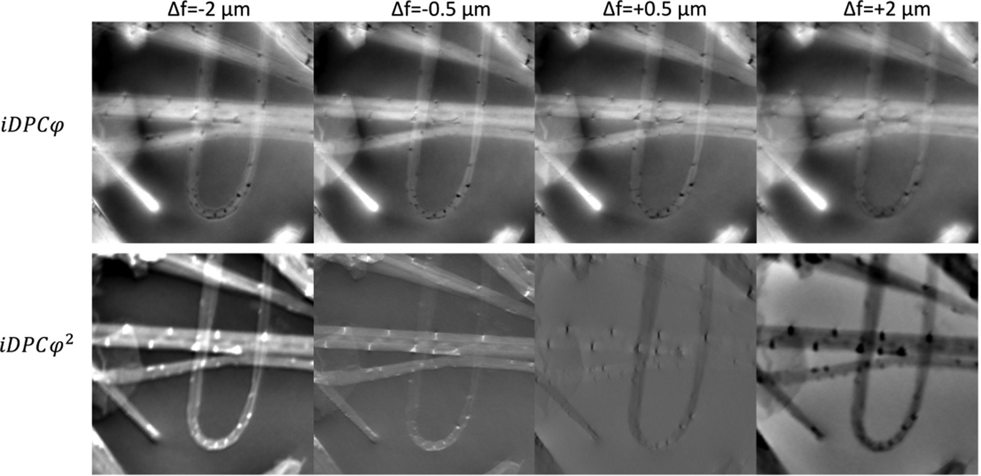
Fig. 6. Separation of iDPC parts reveals a constant part (upper row) related to phase or projected electric potential and a parallax induced part (lower row) related to depth or defocus; objects appear white in underfocus.
Conclusion
The flexible SavvyScan scan system reported here supplements a standard S/TEM and provides improved performance in a number of key areas. As a scan generator, it permits arbitrary scan patterns. Here, we demonstrate scanning with minimal acceleration, as opposed to the conventional raster scan, and develop a correction algorithm to account for the delay of the probe position with respect to the drive signal. As a data collection system, we have eight channels with simultaneous acquisition. We demonstrate the features of the SavvyScan in combination with a new segmented diode detector (Opal). Conventional bright-field and high-angle annular dark-field signals are also recorded. Digitization speed is sufficient for significant oversampling in time, which permits effective interpolation from the unconventional scan patterns to the Cartesian grid of a presentable image. The time stream can be saved for further analysis. The system has been programmed for compatibility with the popular SerialEM software package for microscope control and straightforward integration with sophisticated workflows.
The capabilities of multi-channel recording were explored in various combinations to generate contrast from a weakly scattering specimen of BN nanotubes. Compensation of defocus image shifts from off-axis detector elements provides a simple separation of phase and depth contrast in iDPC. In comparison to iCOM, the method of de-shifted iDPC provides the depth information essentially for free. As these analytical tools are applied post-acquisition, they should be useful as well with other quadrant detectors and even 4D STEM recordings. Looking forward, multi-channel acquisition combined with flexible scan capabilities can offer new sampling approaches in cryo-microscopy for single particle analysis and tomography.
Supplementary material
To view supplementary material for this article, please visit https://doi.org/10.1017/S1431927621012861.
Acknowledgments
The authors gratefully acknowledge the support and advice of David Mastronarde, as well as the generous contribution of his code for plugin/server communication with SerialEM. We thank Lior Segev for initial feasibility studies using Labview. The boron nitride nanotubes were a kind gift of Ernesto Joselevich. This work was supported in part by grants from the Israel Science Foundation, the Weizmann SABRA – Yeda-Sela – WRC Program, the Estate of Emile Mimran, and The Maurice and Vivienne Wohl Biology Endowment. M.E. is the Head of the Irving and Cherna Moskowitz Center for Nano and Bionano Imaging and incumbent of the Sam and Ayala Zacks Professorial Chair in Chemistry. The laboratory has benefited from the historical generosity of the Harold Perlman family.
Appendix A
Accurate calculation of the position of a uniform disk on a quadrant detector in relation to DPC
Assuming the diffraction disk is in focus and is actually uniform, the signal from the detector is proportional to the illuminated area within each quadrant. Adjacent quadrants form a half plane, and the area of intersection A between a round spot and the half plane is analytically determined by the radius R of the spot and the central angle θ measured at the circle center between the vertices of the half plane line cutting the circle.
 $$A = \displaystyle{1 \over 2}R^2( {\theta -\sin \theta } ).$$
In Figure A.1, the relation applies, in one example, to angle θ B and the area of intersection between the diffraction disk and quadrants 1 and 4. The area of one quadrant detector n illuminated by the diffraction disk is proportional to the signal acquired I n. Thus, the following equations are obtained for the ratio of the beam intensity G falling onto opposite half planes:
 $$G_A = \displaystyle{{( {I_1 + I_2} ) -( {I_3 + I_4} ) } \over {I_1 + I_2 + I_3 + I_4}} = \displaystyle{{\theta _A-\sin \theta _A} \over \pi }-1,$$
 $$G_B = \displaystyle{{( {I_1 + I_4} ) -( {I_2 + I_3} ) } \over {I_1 + I_2 + I_3 + I_4}} = \displaystyle{{\theta _B-\sin \theta _B} \over \pi }-1.$$
Fig. A.1. Analysis of the position of the uniform diffraction disk on a quadrant detector.
Using Newton's method with up to 10 iterations, the angles θ A and θ B are determined accurately and rapidly. For example, starting from θ A[0] = πG A + π,
 $$\theta _{A[ {i + 1} ] } = \theta _{A[ i ] }-\displaystyle{{\pi G_A + \pi -\theta _{A[ i ] } + \sin \theta _{A[ i ] }} \over {-1 + \cos \theta _{A[ i ] }}}.$$
As seen in Figure A.1, the isosceles triangles formed by the circle center and the vertices of the circle with x- and y-axes, we realize that
 $$\sin \displaystyle{{\theta _A} \over 2} = \displaystyle{{\sqrt {R^2-x_c^2 } } \over R},$$
 $$\sin \displaystyle{{\theta _B} \over 2} = \displaystyle{{\sqrt {R^2-y_c^2 } } \over R}.$$
 From these equations, it is simple to express the center location x c, y c in terms of the angles and the radius, where the sign of the coordinates is retrieved from the sign of G A and G B. Expanding sinθ A and cosθ A around π provides analytic expressions  $G_A\approx ( 4x_c/\pi R) ( {1-( 1/6) ( x_c^2 /R^2) } )$ and
  $G_B\approx ( 4y_c/\pi R) ( {1-( 1/6) ( y_c^2 /R^2) } )$, showing the quadrature term is absent. The illumination cone in k space corresponds to the radius of the diffraction disk R, the camera length L, and the wavelength λ as k BF = (R/Lλ). Based on the Fourier transform property:
  ${\cal F}_{{\boldsymbol k}_p}{ {{\rm e}^{i2\pi {\boldsymbol q}\cdot {\boldsymbol r}_p}\psi_{in}} } = {\cal F}_{{\boldsymbol k}_p-{\boldsymbol q}}{ {\psi_{in}} }$, with phase gradient 2π q = (∂φ/∂x, ∂φ/∂y) that is nearly constant, the diffracted beam should appear uniform and shifted along the x-axis in according to the vector (∂φ/∂x, ∂φ/∂y).
The known linear approximation of the DPC, namely the phase gradient, can be reproduced as (1/2π)(∂φ/∂x) = q x = (x c/Lλ) ≈ (π/4)G Ak BF and (1/2π)(∂φ/∂y) ≈ (π/4)G Bk BF. The signals G A and G B thus can be related to the DPCx and DPCy signals. The computed center location provides a direct measure of the intensity “center of mass” (COM) displacement for a thin specimen at focus.
We point out that at focus the  ${\rm iDP}{\rm C}_{\varphi ^3}$ term should be related to the third-order correction of the location of the diffraction disk. This leaves the quadratic term
  ${\rm iDP}{\rm C}_{\varphi ^2}$ the main contribution that does not involve the disk location.
Appendix B
Formal relation between parallax offsets and iDPC CTF
In geometrical optics, the wave aberration e−iχ(k) of the condenser lens gives rise to an angular ray deflection resulting in a ray displacement  ${\boldsymbol \delta } = ( 1/2\pi ) {\bf \nabla }_{\boldsymbol k}\chi ( k ) \;$at the plane of the STEM probe. k is the spatial frequency in the diffraction plane, thus δ is, in general, a function of the off-axial position of the detector element. If we assume only defocus ΔZ and no other lens aberrations, δ = λΔZ k. The displacements are introduced to the scanning image depending on the accumulated signal on the detector plane. With the detector sensitivity W(k), we can integrate the related ray displacements to obtain an effective image shift
  ${\boldsymbol S} = \smallint d^2k\;W( {\boldsymbol k} ) {\boldsymbol \delta }( {\boldsymbol k} ) /\smallint d^2k\;W( {\boldsymbol k} )$ with respect to the aberration-free image.
The image shift S for a detector of uniform sensitivity over the x > 0 half plane will be opposite in value compared to the image shift of a detector over x < 0 half plane. So we say that there is a parallax offset between the images of different quadrant detectors and, thus, DPC is affected by the image shift contribution. Yet, if we consider two half planes with a sensitivity similar to a COM sensor, namely W(k) = k x, the two half planes reveal the same S values. This means that the COM sensor is insensitive to the focus-related parallax effect, as it will be for any even aberration in k.
Our purpose is to prove that the CTF of the second term of iDPC is formally related to the difference in image shifts. The main term in  ${\rm CT}{\rm F}_{\varphi ^2}$ of the iDPC image is the integrated CTFc in reciprocal space, related to the cosine of phase contribution to the DPC vector. Without restriction we can consider the x-component based on the detector sensitivity W x(k), a similar result is obtained for the y-component. According to Lazić & Bosch (Reference Lazić, Bosch and Hawkes2017), the calculation is
 $$\overline {{\rm CT}{\rm F}_{c, \;x}} = {-}{\cal F}_{\boldsymbol k}\{ {\psi_{{\rm in}}( {\boldsymbol r} ) {\cal F}_r\{ {W_x{\cal F}_{\boldsymbol k}^{{-}1} \{ {\overline {\psi_{{\rm in}}( {\boldsymbol r} ) } } \} } \} } \} -{\cal F}_{\boldsymbol k}\{ {\overline {\psi_{{\rm in}}( {\boldsymbol r} ) } {\cal F}_r^{{-}1} \{ {W_x{\cal F}_{\boldsymbol k}\{ {\psi_{{\rm in}}( {\boldsymbol r} ) } \} } \} } \}.$$
 Using  $\psi _{{\rm in}}( {\boldsymbol r} ) = {\cal F}_{\boldsymbol r}{ {A( {\boldsymbol k} ) e^{{-}i\chi }} }$ and assuming even aberrations, χ(k) = χ( − k), and a symmetric condenser aperture
  $A( {\boldsymbol k} ) = A( {-{\boldsymbol k}} ) = \overline {A( {\boldsymbol k} ) }$ the calculation is reduced to convolution terms
 $$\overline {{\rm CT}{\rm F}_{c, \;x}} = {-}{\cal F}_{\boldsymbol k}\{ {\psi_{{\rm in}}( {\boldsymbol r} ) } \} \ast [ {W_x( {-{\boldsymbol k}} ) A( {\boldsymbol k} ) {\rm e}^{i\chi }} ] -{\cal F}_{\boldsymbol k}\{ {\overline {\psi_{{\rm in}}( {\boldsymbol r} ) } } \} \ast [ {W_x( {\boldsymbol k} ) A( {\boldsymbol k} ) {\rm e}^{{-}i\chi }} ].$$
For a small aberration phase shift, we can approximate eiχ ≈ 1 + ik x(∂χ/∂k x), hence
 $$\overline {{\rm CT}{\rm F}_{c, \;x}} = {-}{\cal F}_{\boldsymbol k}\{ {\psi_{{\rm in}}( {\boldsymbol r} ) } \} \ast \left[{W_x( {-{\boldsymbol k}} ) A( {\boldsymbol k} ) ik_x\displaystyle{{\partial \chi } \over {\partial k_x}}} \right] + {\cal F}_{\boldsymbol k}\{ {\overline {\psi_{{\rm in}}( {\boldsymbol r} ) } } \} \ast \left[{W_x( {\boldsymbol k} ) A( {\boldsymbol k} ) ik_x\displaystyle{{\partial \chi } \over {\partial k_x}}} \right].$$
Ignoring the convolution with the probe, the CTF can be integrated over x- and y-components via
 $${\rm CT}{\rm F}_{\varphi ^2}\approx {\rm CT}{\rm F}_{{ic}} = \displaystyle{{{\rm CT}{\rm F}_{c, x}} \over {2\pi ik_x}} + \displaystyle{{{\rm CT}{\rm F}_{c, y}} \over {2\pi ik_y}}.$$
Approaching k → 0, the convolution is replaced with integration over k space, therefore
 $${\rm CT}{\rm F}_{\varphi ^2}( {{\boldsymbol k} = 0} )$$
 $$\approx \displaystyle{1 \over {2\pi }}\int {\int {dk_xdk_y\vert A( {\boldsymbol k} ) \vert ^2\{ \displaystyle{{\partial \chi } \over {\partial k_x}}[ {W_x( {\boldsymbol k} ) -W_x( {-{\boldsymbol k}} ) } ] + \displaystyle{{\partial \chi } \over {\partial k_y}}[ {W_y( {\boldsymbol k} ) -W_y( {-{\boldsymbol k}} ) } ] \} } }$$
 $$\propto ( {S_x^ + {-}S_x^- } ) + ( {S_y^ + {-}S_y^- } )$$
 Written in this form, we observe that  ${\rm CT}{\rm F}_{\varphi ^2}$ at a low spatial frequency is proportional to the sum of image shift differences between the left and right quadrants as well as the image shifts between the upper and lower quadrants of the DPC detector. Thus, in the absence of lens aberrations, the CTFφ 2 of any symmetric four quadrant segments is expected to read
  ${\rm CT}{\rm F}_{\varphi ^2}\propto k {\rm \Delta }Z + O( k{\rm \Delta }Z) ^2$.


 Open access