


Introduction
Over the last decade, outstanding progress has been made concerning the imaging of nanomaterials at atomic resolution. Arguably, a mature aberration-correction technology (Hawkes, Reference Hawkes2015) enables the identification of most single atoms from the periodic table of elements in three dimensions (Chen et al., Reference Chen, Van Dyck and Kisielowski2016; Miao et al., Reference Miao, Ercius and Billinge2016). The precision to measure atom coordinates can reach the 1.9 pm wavelength (λ) limit for relativistic electrons accelerated by 300 kV if the recorded image contrast is adequate (Specht & Kisielowski, Reference Specht and Kisielowski2017). A spectacular resolution around half the diameter of a hydrogen atom is demonstrated by aberration-corrected electron microscopy even though the remaining objective lens aberrations still limit the resolution in electron microscopy to roughly 20*λ (Erni et al., Reference Erni, Rossell, Kisielowski and Dahmen2009).
Routine applications of this capability, however, remain challenging because achieving high contrast at atomic resolution requires the deposition of an extraordinary large power density by the impinging electrons, and this alters the observed object (Kisielowski et al., Reference Kisielowski, Wang, Specht, Calderon, Barton, Jiang, Kang and Cieslinski2013). While this aspect can occasionally be ignored in investigations of classic bulk materials, the research frontiers have moved to include radiation-sensitive matter, where awareness of electron-beam-induced object alterations becomes essential (Kisielowski, Reference Kisielowski2016). In biological sciences, for example, a suitable level of damage control is rigorously enforced by limiting the accumulated electron dose, d A, to gain a reproducible structure determination of proteins by cryogenic electron microscopy (cryo-EM) (Henderson, Reference Henderson2018). Moreover, time-resolved electron microscopy emerges (4D-EM) (Flannigan & Zewail, Reference Flannigan and Zewail2012), which stimulates interest in studying dynamic processes that lead to functional behavior. In those cases, beam–sample interactions have become a considerable bottleneck (Egerton, Reference Egerton2019).
From a practical point of view, critical parameters to assess electron-beam-induced damage can be related to the deposited electron charge C, which is given by the following equation:
 $$C = N \,\raise-2.5pt{\hbox{\ast}}\, e = d_{\rm A}\,\raise-2.5pt{\hbox{\ast}}\, F_{\rm I} = I \,\raise-2.5pt{\hbox{\ast}}\, t = d_{\rm R} \,\raise-2.5pt{\hbox{\ast}}\, F_{\rm I}\,\raise-2.5pt{\hbox{\ast}}\,t , $$
where N*e is the charge of N electrons, d A (e/Å2) is the accumulated electron dose, F I (Å2) is the area irradiated by the electron beam current I (e/s), t is the time, and d R (e/Å2/s) is the dose rate.
It is not surprising that the different scientific communities make the use of relation (1) in ways that best meet their needs. In biological research, the accumulated dose d A = C/F I is the most critical parameter because it was determined that the deposition of only a few electrons per square Ångström suffices to reduce diffraction intensities of organic crystals. This diffraction amplitude reduction is typically quantified as the d A required to reach 1/e of the initial diffraction intensity (Henderson & Glaeser, Reference Henderson and Glaeser1985). It is assumed that this beam-induced intensity reduction is independent of the irradiated area and occurs instantaneously with the onset of sample irradiation because it is driven by ionization cross-sections (Van Dyck & Wilkens, Reference Van Dyck and Wilkens1984). Exceptions to this general expectation are documented (Siegel, Reference Siegel1972; Bullough & Henderson, Reference Bullough and Henderson1987).
On the other hand, the beam current I is a critical parameter in 4D-EM that operates in space and time [r = r(x,y,z,t)] (Flannigan & Zewail, Reference Flannigan and Zewail2012) and relates to the deposited charge by I*t = C. Existing instrumentation currently approaches atomic resolution in real-space images, with a time resolution of attoseconds (Feist et al., Reference Feist, Echternkamp, Schauss, Yalunin, Schaefer and Ropers2015). It opens an exciting path to study dynamic material responses even at quantum limits and, in combination with modeling, provides improved insight into beam–sample interactions (Nordlund et al., Reference Nordlund, Zinkle, Sand, Granberg, Averback, Stoller, Suzudo, Malerba, Banhart, Weber, Willaime, Dudarev and Simeone2018). Unexpectedly, pronounced retardation of beam damage emerges as an additional benefit of operating pulsed electron beams. The effect was attributed to a time modulation of phonon excitations (Kisielowski et al., Reference Kisielowski, Specht, Freitag, Kieft, Verhoeven, van Rens, Mutsaers, Luiten, Rozeveld, Kang, McKenna, Nickias and Yancey2019; VandenBussche & Flannigan, Reference VandenBussche and Flannigan2019).
In material sciences, however, it is common that neither the accumulated electron dose nor the applied beam current is explicitly recognized as a critical parameter because the existence of sample damage can be subtle. For example, knock-on damage (McKinley & Feshbach, Reference McKinley and Feshbach1948) initiates atom displacements. But their resulting motion is fast compared to recording times, (Surrey et al., Reference Surrey, Pohl, Schultz and Rellinghaus2012) and their intensity contribution to the contrast of atom columns is thickness dependent and often small (Chen et al., Reference Chen, Van Dyck and Kisielowski2016), which makes their displacements hard to detect. An accumulated electron dose (d A) that easily exceeds 104 e/Å2 is routinely applied in the context of electron tomography with atomic resolution (Chen et al., Reference Chen, Van Dyck and Kisielowski2016; Miao et al., Reference Miao, Ercius and Billinge2016) where it is needed to detect single atoms above the noise. Indeed, the application of a high accumulated electron dose could be without consequences if knock-on damage were the only degradation mechanism and if only heavy atoms with strong bonds to crystal sites were considered (McKinley & Feshbach, Reference McKinley and Feshbach1948). However, structural alterations become disturbingly relevant during observation of small crystals (≲5 nm), surfaces, interfaces, or other crystal defects (Kisielowski, Reference Kisielowski2015), or if amorphous structures are investigated (Rezikyan et al., Reference Rezikyan, Jibben, Rock, Zhao, Koeck, Nemanich and Treacy2015) that tend to locally crystallize in the electron beam (Kisielowski et al., Reference Kisielowski, Specht, Gygax, Barton, Calderon, Kang and Cieslinski2015). Here, atom binding energies and their coupling to excited states vary greatly while ionization effects persist so that a hard damage threshold for mid-voltage electrons (20–300 kV) hardly exists (Jiang & Spence, Reference Jiang and Spence2012; Specht & Kisielowski, Reference Specht and Kisielowski2017; Kretschmer et al., Reference Kretschmer, Lehnert, Kaiser and Krasheninnikov2020). In fact, it can become impossible to determine if specific imaged material features are still pristine or were altered by beam–sample interactions. In addition, the size of the irradiated area, F I, changes dramatically depending on whether or not a focused probe is scanned across a sample (F I = 1–100 Å2) or parallel illumination (F I = 106–109 Å2) is applied. A few publications report the advantage of beam current variations to establish material-specific threshold values. Examples include a reliable determination of the charge state of vanadium atoms at oxide surfaces (Ek et al., Reference Ek, Ramasse, Arnarson, Moses and Helveg2017) or maintaining the structural stability of small gold crystals in low dose rate conditions, (Kisielowski, Reference Kisielowski2015) which is otherwise challenging to achieve (Knez et al., Reference Knez, Schnedlitz, Lasserus, Schiffmann, Ernst and Hofer2018).
It is desirable to embrace the rich technological opportunities that advanced electron microscopes offer to clarify in which circumstances the deposited charge or the beam current drives structural alterations at the atomic scale. This paper describes how direct imaging and electron diffraction in broad-beam mode can be optimized to achieve this goal without compromising high spatiotemporal resolution or the ability to detect single-electron scattering events. Simultaneously, the approach embraces the low-dose region, which is critical for cryo-EM applications. We find that in the ultimate detection limit where N = 1 in equation (1) and only single electrons and their self-interference are captured, both the accumulated electron dose and the dose rate become parameters that can modulate beam–sample interactions. Time and the size of the irradiated area link them to charge and beam current as required by equation (1).
Materials and Methods
Optoelectronic components of electron microscopes are intimately linked to their intended application. Figure 1 highlights selected instrument features that are of relevance here.
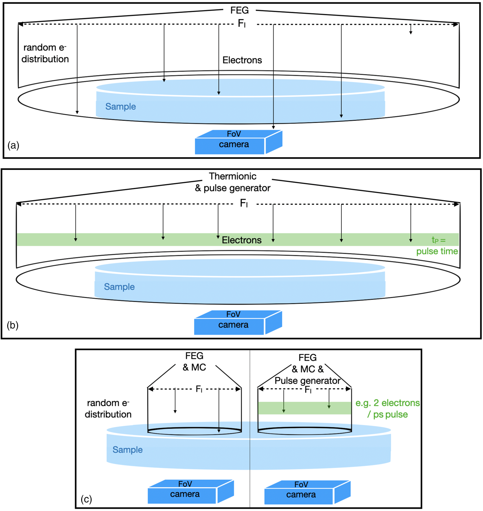
Fig. 1. Schematic features of selected microscope configurations. (a) Cryo-EM or high-resolution transmission electron microscopy, irradiated area (F I) > sample > FoV; the deposited charge is C = d A*F I; the electron distribution is random in time. Electrons that do not hit the sample are wasted. (b) 4D electron microscopy; same as (a) but equipped with a thermionic gun, the electron beam is structured in the time domain so that they arrive at the sample in pulses, 6 electrons/pulse are indicated. The deposited charge is C = I*t. (c) This work: pencil-like illumination with parallel beam (or STEM if focused). F I ≂ FoV < sample; the deposited charge is C = I*t = d A*F I = d R*F I*t; the relation between d A and d R can be studied; left: random electron distribution; right: electron distribution structured in time.
In biological cryo-EM (Fig. 1a), electrons are randomly emitted from a field emission gun (FEG), and a condenser system distributes them with equal intensity over a large irradiated area (F I). The field of view (FoV) is normally adjusted to match the size of the camera entrance aperture and can be much smaller than F I. Therefore, the size of the camera entrance aperture and its performance are of critical concern in cryo-EM (Grob et al., Reference Grob, Bean, Typke, Li, Nogales and Glaeser2013). The same setup is used for traditional high-resolution transmission electron microscopy (HRTEM), where the accumulated electron dose easily exceeds 10,000 e/Å2. In stark contrast, atomic resolution imaging of pristine soft matter is only achievable if the accumulated dose, d A, is kept below ~10 e/Å2 (Zhang et al., Reference Zhang, Zhu, Liu, Ying, Hsiung, Sougrat, Li and Han2018).
In 4D electron microscopy (Fig. 1b), the time modulation of the electron beam is either stimulated by laser pulses that assist photoelectron emission from a thermionic filament (Flannigan & Zewail, Reference Flannigan and Zewail2012) or by periodically deflecting the continuous electron flow from a field emission source at ultra-high frequencies (Verhoeven et al., Reference Verhoeven, van Rens, Kieft, Mutsaers and Luiten2018). Ideally, it is attempted to include only 1 e in each pulse that hits the sample during the pulse duration in order to avoid the Coulomb interaction of the negatively charged electrons at the source. Since the number of electrons in each pulse is kept small, beam current variations are achieved by altering the delay time between pulses. Therefore, the beam current is a critical parameter in such experiments that relate to the dose rate, d R.
Our experiments make use of a Nelsonian illumination scheme (Tiemeijer et al., Reference Tiemeijer, Bischoff, Freitag and Kisielowski2012), a Cc corrector (Kabius et al., Reference Kabius, Hartel, Haider, Müller, Uhlemann, Loebau, Zach and Rose2009), and a K2 camera (Grob et al., Reference Grob, Bean, Typke, Li, Nogales and Glaeser2013) that were installed in the transmission electron aberration-corrected microscope TEAM I. This setup is schematized in the left part of Figure 1c. The Nelsonian illumination scheme creates a remarkably coherent (ΔE: 100 meV), pencil-like illumination rod of a diameter that can be matched to the FoV of the K2 camera (106–107 Å2), while detecting single-electron scattering events and maintaining atomic resolution capability with a magnification-dependent image pixel size around 0.3×0.3 Å2. Furthermore, low-dose experiments benefit from the ability to quickly change the beam current (<1 s) by orders of magnitude without an introduction of uncontrolled lens aberrations (Kisielowski et al., Reference Kisielowski, Specht, Gygax, Barton, Calderon, Kang and Cieslinski2015). In addition, the Cc corrector enhances phase-contrast because it focuses all coherently scattered electrons into the same image plane, even if energy losses as large as ~600 eV occur (Kabius et al., Reference Kabius, Hartel, Haider, Müller, Uhlemann, Loebau, Zach and Rose2009). These characteristics are advantageous for the imaging of organic matter where plasmon losses can largely dominate over the zero-loss intensity. Previously, it was demonstrated that the approach is fully compatible with pulsed-beam operations (Kisielowski et al., Reference Kisielowski, Specht, Freitag, Kieft, Verhoeven, van Rens, Mutsaers, Luiten, Rozeveld, Kang, McKenna, Nickias and Yancey2019) (Fig. 1c, right), and it can naturally be extended to include scanning capabilities (Dwyer et al., Reference Dwyer, Kirkland, Hartel, Müller and Haider2007). In fact, it can be seen as a hybrid configuration to pursue scanning and broad beam experiments. It is somewhat unusual to operate the TEAM I microscope with a Cc corrector and a monochromator because both optoelectronic components were previously regarded as exclusive alternatives to enhance resolution. Here, they are used together to address beam–sample interactions. We note that in absence of beam pulsing capabilities, average information about time dependences can still be estimated from beam current variations because their inverse value provides an average delay time per electron that successively interacts with the sample.
If a critical accumulated dose can be increased by dose fractionation or if time resolution is pursued, the acquisition of image series becomes a necessity. Drawbacks relate to the creation of large data sets: if the K2 camera is employed (3,710 × 3,838 pixels/image) to record a series of 50 images, 2.6 GB of storage space is required that must be processed to provide a single image. Moreover, there is a well-known uncertainty in setting appropriate focus values in low-dose conditions because interpretable information may only become visible after image recording and processing, without the ability to produce a second image of the same area. We ease this uncertainty by capturing focal series of images. If averaged, a focal series provides a single HRTEM image for immediate inspection where the depth of the focal series Δf = f max−f min becomes the resolution-limiting factor because it exceeds the narrow focus spread (10–15 Å) of the TEAM microscopes (Kisielowski, Reference Kisielowski2016). It is well understood that the contrast transfer function modulates the image contrast of any HRTEM image. Thus, it remains unknown how to relate contrast to atom positions in the average image. However, it is well established how to remove this ambiguity offline by reconstructing the electron exit wave function from a recorded focal series using the Tempas software package (Kilaas, Reference Kilaas2021). This program is also used for all other image processing and for simulations. A reconstructed electron exit wave function provides element-specific atom positions in three dimensions from single projections (Chen et al., Reference Chen, Van Dyck and Kisielowski2016) and can even remove residual lens aberrations by applying a numerical phase plate. In addition, low spatial frequencies can be captured by recording images at large defocus values (Haigh et al., Reference Haigh, Jiang, Alloyeau, Kisielowski and Kirkland2013), which boosts phase contrast at low spatial frequencies to a similar extent as a physical phase plate (Alloyeau et al., Reference Alloyeau, Hsieh, Anderson, Hilken, Benner, Meng, Chen and Kisielowski2010). Necessarily, image drift must be removed from any image series. We use the cross- and phase-correlation methods in the Tempas software to align the entire series with sub-pixel accuracy. However, if discrete scattering events occur, image misalignments become significant if a substantial number of pixels remain void. Therefore, we choose beam currents large enough to capture at least 1 e in each pixel on average. This requirement translates into a minimum accumulated electron dose of 4 e/Å2 per real space image if 1 Å2 is sampled by 2 × 2 pixels. A dose rate of 4 e/Å2/s at 1 Å resolution is small enough to avoid structure modification in important materials that are radiation-sensitive (Zhang et al., Reference Zhang, Zhu, Liu, Ying, Hsiung, Sougrat, Li and Han2018) but it remains to be a considerable accumulated dose if organic substances are considered. As a result, experiments with organic substances are often performed by sacrificing resolution.
In diffraction mode, the accumulated electron dose can be reduced by another three orders of magnitude if single crystals are investigated because electrons must only be captured at the location of the diffraction spots. Figure 2a shows the historic double-slit experiments where electron holography is used to unmask the wave-particle dualism of single electrons at the ultimate detection limit where quantum mechanical principles apply. Single-electron scattering in crystals follows the same principal because their wave functions interact with the periodic crystal potential before they collapse into single particles at the detector (Fig. 2b). The result is the statistical buildup of intensity by single-electron scattering events within the envelope function of the diffraction pattern which can be observed due to self-interfering electrons. This provides the opportunity to study how a diffraction pattern emerges as a window into quantum mechanics instead of merely probing how diffraction spots decay as a result of beam–sample interactions. This comparison is pursued in this paper.

Fig. 2. Building diffraction patterns by self-interfering single electrons at the ultimate detection limit. (a) Holographic experiment that makes use of a bi-prism to build up the diffraction pattern of a double slit. The two images at time t 1 < t 2 were reported by Lichte (Reference Lichte1978). (b) Adaptation of the same idea to electron scattering in crystalline solids where electron waves interfere with the wave functions of the crystal (cylinders) and themselves but the diffraction pattern (blue) is built up by summing up electron particles (red) in time.
Beam currents are calibrated by Faraday cups and by counting electrons in the single-electron detection mode of the K2 camera. For a direct electron detector to work in single-electron counting mode, the electron flux per pixel cannot exceed ~10 e/s. We stay below this maximum electron count throughout this paper. This is possible because any desired accumulation of electron dose can be captured in image series with variable dose rates to study materials with very different responses to radiation which are investigated at the Molecular Foundry. Examples for the imaging mode include exotic materials such as ammonium hydrogen urate (NH4HU), which is the main component of kidney stones in Bottlenose dolphins. MoxSy nanowires of unknown stoichiometry are analyzed, which were grown by a vapor–liquid–solid technique from a gold seed at 800°C.
A double metal cyanide (DMC) material (Wojdeł et al., Reference Wojdeł, Bromley, Illas and Jansen2007) is at the core of our research interests and is an optimal choice for diffraction work. The single crystals are prepared chemically, and they exhibit facets of lateral dimensions around 500 nm. They crystalize in the monoclinic space group Pm (#6) and are stable during air exposure. DMC crystals are shown in Figure 3 in low-magnification/low-dose imaging conditions that reveal flat surfaces and a pronounced preference to attach the (001) plane to the lacey carbon mesh of the transmission electron microscopy (TEM) grid. This geometry is advantageous because it eliminates the need to align the [001] crystal orientation with the electron beam for each crystal flake. Moreover, a reasonably homogeneous crystal thickness of roughly 200 nm in the [001] direction allows comparing diffraction intensities quantitatively as long as F I is kept smaller than the lateral crystal dimensions (Fig. 3a).

Fig. 3. Low magnification images of the investigated DMC crystals deposited on a lacey carbon substrate and detected by 0.02 e/Å2/s. At low magnification the crystals are hardly visible but radiation damage becomes negligible during searches. (a–c) Defocused images recordings with an UltraScan camera. For reference, the FoV of the K2 camera system is indicated in (a). The diameter of the Nelsonian illumination system matches this size in our high-resolution and diffraction work. F I ≂ FoV < sample. (d) Focused recording that highlights the noise suppression by the K2 camera.
DMC materials were synthesized following a recipe developed at Dow. Briefly, its synthesis includes the following steps: (1) Prepare solution A by dissolving 11.4 g ZnCl2 in 11.4 g H2O; prepare solution B by dissolving 1.11 g K3[Co(CN)6] in 45.3 g H2O and 5.85 g tert-butanol (t-BuOH). (2) Add solution B to a beaker in a water bath at 30°C, with mechanical stirring at 250 rpm. (3) Add solution A to solution B to initiate the precipitation reaction. A slurry mixture is formed. (4) After the complete addition of solution A, allow the slurry to stir for 30 min. (5) Pour the mixture into centrifuge tubes and centrifuge at 8,000 rpm for 30 min. (6) Decant the supernatant and disperse the solid in a mixture of t-BuOH and water while stirring at 250 rpm for 30 min. (7) Pour the mixture into centrifuge tubes and centrifuge at 8,000 rpm for 30 min. (8) Decant the supernatant, disperse the solid again in a mixture of t-BuOH and water, and stir at 250 rpm for 30 min. (9) Pour the mixture into centrifuge tubes and centrifuge at 8,000 rpm for 30 min. (10) Decant the supernatant and dry the solid for 16 h in a vacuum oven at ~25 mbar at 50°C. (11) Grind the powder in a mortar to break up agglomerates. The material is then ready for characterization. All chemicals were purchased from Sigma-Aldrich and used without further purification. The prepared crystals were loaded on lacey carbon grids, pre-screened, and pre-investigated with Dow's ThermoFisher Titan TEM (Kisielowski et al., Reference Kisielowski, Specht, Freitag, Kieft, Verhoeven, van Rens, Mutsaers, Luiten, Rozeveld, Kang, McKenna, Nickias and Yancey2019).
Results and Discussion
The investigated materials are chosen from different research backgrounds to include material sciences (MoxSy), biological applications (NH4HU), and chemical sciences (DMC catalyst) stressing the ability of the approach to pursue interdisciplinary research into functional materials. Each example takes advantage of current state-of-the-art imaging to investigate materials with single-electron detectors, the ability to accommodate dependences on the accumulated electron dose or the dose rate, if present, and the potential for time-resolved studies. They are discussed in order of growing challenges. The first example is closest to a traditional HRTEM recording and describes research into MoxSy, which has attracted significant interest because of its designable electronic and optoelectronic properties (Wang et al., Reference Wang, Kalantar-Zadeh, Kis, Coleman and Strano2012) and its pronounced catalytic activity (Zhu et al., Reference Zhu, Ramasse, Brorson, Moses, Hansen, Kisielowski and Helveg2014). Electron irradiation of MoxSy is known to continuously alter atomic configurations in proximity to the surface where a hard threshold to beam damage does not exist (Kretschmer et al., Reference Kretschmer, Lehnert, Kaiser and Krasheninnikov2020). Here, it is demonstrated that even if the material is radiation-sensitive, defects and buried interfaces can be imaged at atomic resolution while enhancing control of beam damage by choosing a suitable low dose rate. Figure 4a shows the averaged focal series image of a MoxSy nanorod grown from a gold seed that is visible at the top of the nanorod. We chose to record a focus series of 50 images over a focal depth of Δf = 500 Å with an average count of 19 e/image pixel of 0.32 Å2 size. An image drift = 0.35 Å/s was determined by image correlation, which allows for an exposure time of 2 s while maintaining sub-Ångström resolution. These conditions provide a FoV that equals 4.5 106 Å2, a dose rate d R of 185 e/Å2/s, and an accumulated dose d A that reaches 18,500 e/Å2. Thus, the accumulated electron dose is high enough to detect single atoms. A beam current of 63 pA is comparable with scanning transmission electron microscopy (STEM) investigations where the dose rate would be orders of magnitude higher because the irradiated area would be about a square Ångström. Sub-Ångström resolution is maintained across the large FoV, and the magnified inset in Figure 4a is used to highlight the presence of lattice fringes everywhere. Image delocalization is most prominent at the Au/MoxSy interface and is caused by Δf. Moreover, Moiré fringes appear in the region of material overlap that terminates at a buried interface. The location of the Au/MoS2 interface is unknown within the thickness of the sample.
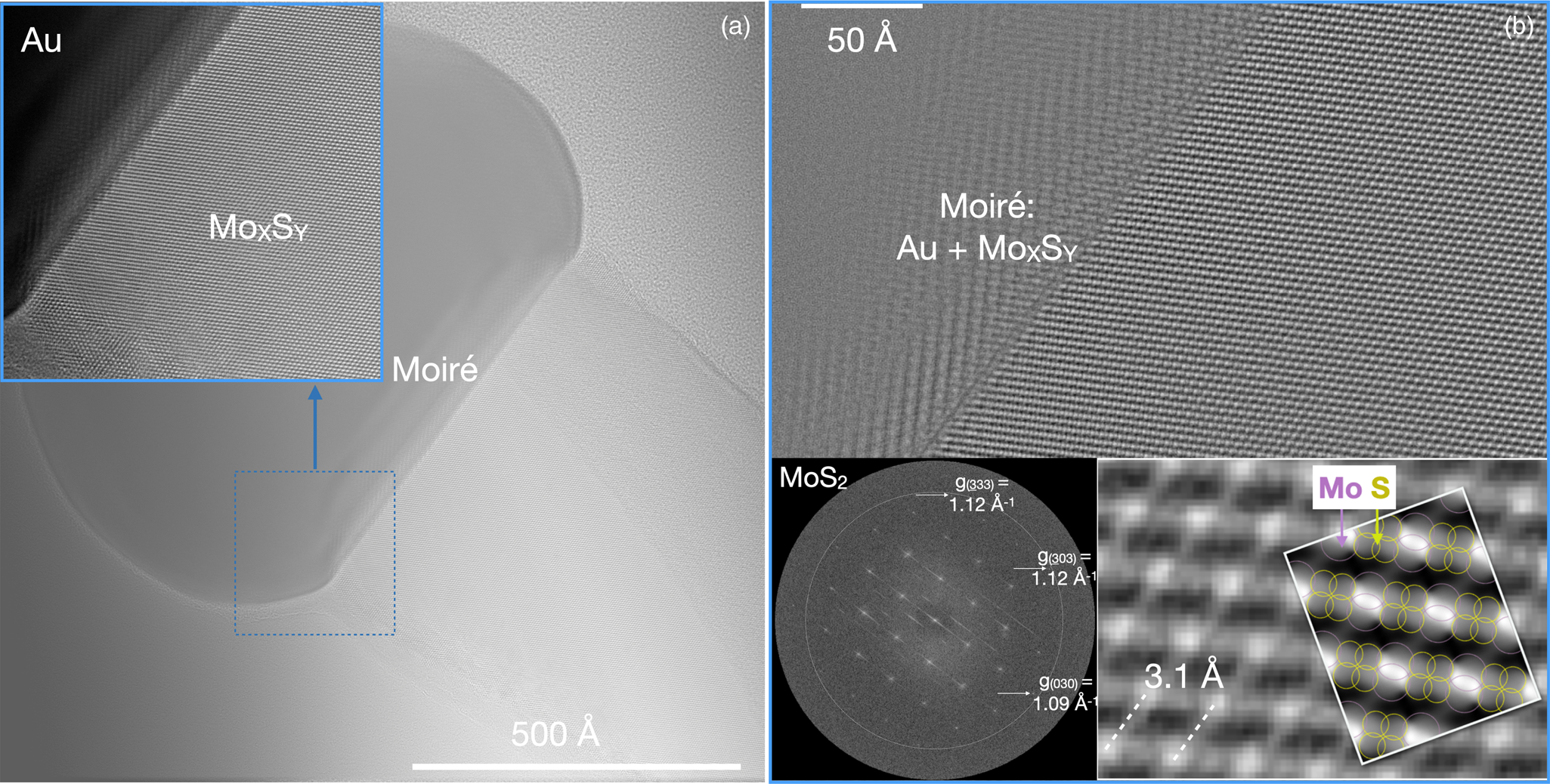
Fig. 4. Low dose rate imaging of an MoS2 nanorod grown from a gold seed. Imaging parameters: 50 images; Δf = (510 − 52) Å; image drift = 0.35 Å/s; counts = 19 e/pixel/s; image pixel size = 0.32 Å/pixel; d R = 185 e/Å2/s; d A = 18,500 e/Å2; FoV = 1.4*106 Å2, F I = 1.5*FoV; I = 63 pA. (a) Averaged lattice image providing an overview while maintaining sub-Ångstrom resolution everywhere, which becomes visible if areas of interest are magnified (inset). (b) Reconstructed phase image of the electron exit wave function focused at the Au/MoxSy interface. Insets: the nano-diffraction pattern calculated from the Fourier transform of the wave function is compatible with hexagonal [101] MoS2 and magnified phase image with a simulated phase for 700 Å thick hexagonal [101] MoxSy. The atom columns are labeled by circles and their phase signal is broadened because of the large sample thickness.
In Figure 4b, the reconstructed phase of the electron exit wave function is shown, which removes all delocalization effects at the Au/MoxSy interface if it is focused by wave propagation (Chen et al., Reference Chen, Van Dyck and Kisielowski2016). As a result, the buried interface is shown to be atomically abrupt. This is information that cannot be obtained otherwise. The Fourier transform of the exit wave function provides the nano-diffraction pattern of the inset with diffraction spots that reach beyond 1 Å. The 0.03 Å−1 difference between the g(333) = g(303) = 1.12 Å−1 and g(030) = 1.09 Å−1 reflections suggest a [101] zone axis orientation if hexagonal MoS2 is assumed (Dickinson & Pauling, Reference Dickinson and Pauling1923). Supporting this interpretation, the electron exit wave function is simulated to mimic the experimental phase image at a crystal thickness of 700 ± 13 Å as shown by the second inset in Figure 4b. However, the atomic columns remain unresolved because of phase signal broadening with increasing crystal thickness, which can hide structural variations. Because the sample is thick, surface alterations by the electron beam remain hidden, even if present, but a possible stimulation of beam-induced inter-diffusion (Zheng et al., Reference Zheng, Sadtler, Habenicht, Freitag, Alivisatos and Kisielowski2013) at the Au/MoxSy interface does not occur at the chosen low dose rate.
Another extreme is shown in Figure 5 where low dose rate images from ammonium hydrogen urate (NH4HU) are presented. The ability to capture such an image is remarkable because a dose accumulation of ~50 e/Å2 in a second wipes out all information about its atomic structure. Such single crystals are studied because the development of kidney stone disease in dolphins caused significant morbidity and mortality and has become one of the major threats to survival of Bottlenose dolphins. The presence of NH4 makes the material radiation-sensitive, and cryo-EM could be an appropriate choice to study the material. Moreover, rapid sample shrinkage occurs in the electron beam if the material is exposed to a dose rate of d R = 185 e/Å2/s as used in the previous example. That is common in frozen-hydrated biological materials (Typke et al., Reference Typke, Gilpin, Downing and Glaeser2007) and is often attributed to beam-induced hydrogen losses (Glaeser, Reference Glaeser2016). Only a reduction of the beam current to 8 pA and imaging with a dose rate of only 13 e/Å2/s allow for the acquisition of the single HRTEM image of Figure 5a. It reveals a perfect crystal structure, but the contrast is shot-noise dominated. Consistent with our past experience of reconstructing the wave function of the radiation-sensitive magnesium chloride, (Kisielowski, Reference Kisielowski, Specht, Freitag, Kieft, Verhoeven, van Rens, Mutsaers, Luiten, Rozeveld, Kang, McKenna, Nickias and Yancey2019) a total dose of 130 e/Å2 can be accumulated by dose fractionation to produce the average image of Figure 5b. The image drift is only 0.67 Å/s. Consistent with the low drift values, beam-induced sample alterations remain negligible, and the signal-to-noise ratio in Figure 5b is greatly enhanced by image averaging. As a result, image Fourier components between 1.4 and 14 Å are transmitted by the Cc-corrected objective lens, which is extraordinary for a radiation soft matter and is amplified by the corrector's ability to focus all inelastically scattered electrons up to 600 eV into the same image plane.

Fig. 5. Low dose rate imaging of radiation-sensitive NH4HU single crystals. Imaging parameters: ten images; Δf = 0 Å; image drift = 0.67 Å/s; counts = 2.3 e/pixel/s; image pixel size = 0.42 Å/pixel; d R = 13 e/Å2/s; d A = 130 e/Å2; FoV = 2.6*106 Å2; F I = 1.5*FoV, I = 8 pA. (a) Single-shot noise-dominated single image, d A = 13 e/Å2. (b) Average of ten images, d A = 130 e/Å2, Δf ~ 250 Å. The inserted Fourier transform demonstrates information transfer between 1.4 and 14 Å, where the low-frequency edge can be extended by recording at larger defocus values.
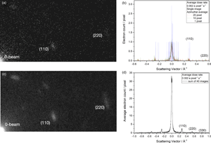
The current limit for the creation of real space images from dose-fractionated image series with low dose rates is the inability to align the images if they are exposed by less than ~1 e/image pixel. Independent of possible solutions to this problem, the beam current can be reduced by another three orders of magnitude if diffraction patterns are dose-fractionated because electron diffraction is insensitive to lateral sample translations. We use the DMC material for this purpose because its diffraction pattern vanishes in the electron beam if d A exceeds 5 e/Å2. A beam current of only 1 fA is used to record the diffraction pattern of Figure 6a. Single-electron scattering events are seen that produce a binary (telegraph) signal of integer numbers as shown by the single-pixel line profile of Figure 6b. It is seen that single electrons are detected well above the noise. For analysis, we smooth this telegraph signal by an azimuthal average over a few pixels to obtain the recognizable diffraction profiles as shown in the figure. Since void pixels are included in the average, the electron count drops well below 1 e/pixel in the diffraction spots. Moreover, the low beam current ensures that only electron self-interferences are detected, in perfect analogy to holographic experiments that use a bi-prism to build up a diffraction pattern of a double slit (see Fig. 2). The diffraction pattern of Figure 6c shows that electron accumulation occurs at the expected positions of diffraction spots that can be calculated from the scattered electron wave function and its interaction with the periodic crystal potential of DMC. Higher-order reflections emerge from noise upon summing successively recorded images so that the creation of a diffraction profile as shown in Figure 6d can be studied in detail instead of simply recording the decay of diffraction spots as a result of beam–sample interactions. This comparison is made next.
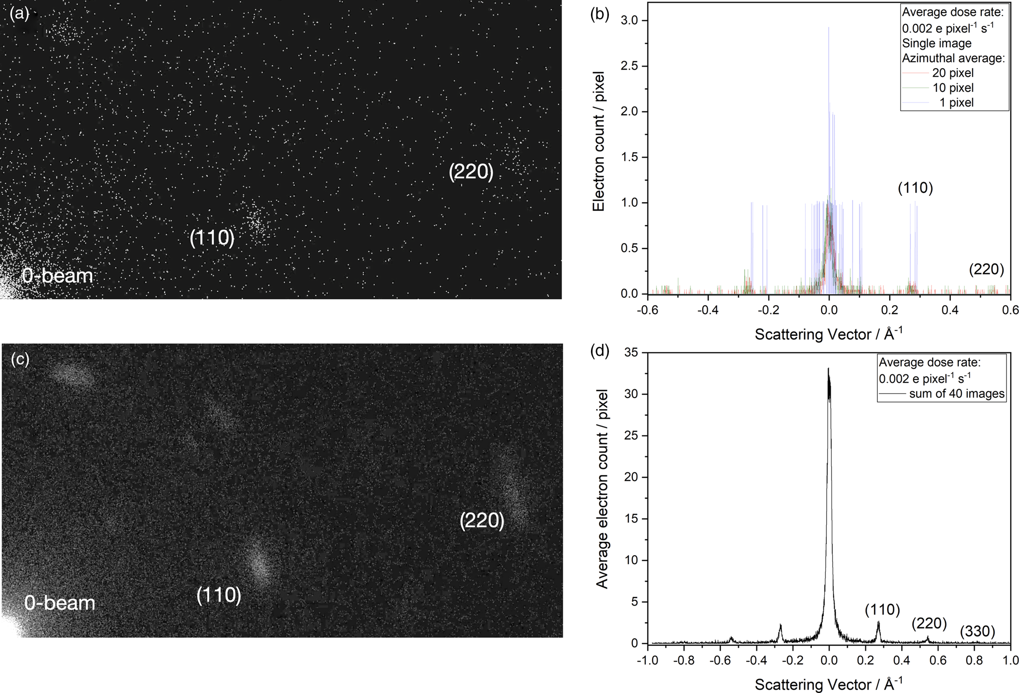
Fig. 6. Electron diffraction of DMC at the ultimate detection limit (Kisielowski et al., Reference Kisielowski, Specht, Yancey, Rozeveld, Kang, McKenna and Barton2020). The beam current is 1 fA and the dose rate is 0.002 e/pixel/s. (a) A diffraction pattern where the detection of electrons (particles) accumulate at locations of diffraction spots that are predictable because electrons have wave character (wave-particle dualism). (b) Single-pixel line profiles show integer electron counts with the K2 camera of a large S/N ratio. The telegraph signal can be smoothed by azimuthal averages as indicated. (c) Building up a diffraction pattern by summing 40 recordings as in (a) and using an azimuthal average of 20 pixels. (d) Line profile across the sum of the diffraction patterns, where the zero beam is not saturated and the higher-order diffraction peaks emerge. In this case, the diffraction pattern is built up to record a reciprocal distance of ~1 Å−1 with average counts well below 1 e/pixel.
Figure 7a shows an indexed diffraction pattern of DMC that was recorded with the microscope configuration depicted in Figure 1a. This enabled the study of fading diffraction spots with dose accumulation. The recording is at room temperature. The line profile of Figure 7c demonstrates that the electron count reaches into the thousands. A multitude of counts are created by irradiating a large crystal area (3.1 * 109 Å2) with a medium beam current (37 pA), thus obtaining a low dose rate (0.07 e/Å2/s) that allows tracking the decay of the (110) diffraction spots to their 1/e value at a critical accumulated dose of only 5 e/Å2. All higher-order diffraction spots decay faster. Figure 7b shows the same diffraction pattern of DMC, but recorded with the modified microscope configuration of Figure 1c. Black circles are used to show that a kinematic calculation of a selected area diffraction pattern matches the experiment if Wojdeł's model for DMC is used. Visually, both recordings are quite similar except for a somewhat different diffraction peak width. However, the vast differences between the recording techniques become obvious if absolute values are compared: the irradiated area is reduced 200-fold and the beam current by factors of 220 and 6,200, creating a dose rate that is ultra-low. As a result, required electron counts for the emerging (110) diffraction intensity drop into single digits that are only detectable with advanced camera systems. It is unexpected but welcome that the (110) intensity builds up almost linearly with dose accumulation so that there is only marginal intensity loss at an accumulated dose of 5 e/Å2, while the same signal was destroyed when the traditional recording technique was used. Thus, critical 1/e values for the accumulated electron dose reach beyond the x-scale of Figure 7d. Moreover, the signal intensity becomes dose rate dependent because the average delay time between successive electrons is reduced from 3 μs/e to 100 ns/e. At this point, structural transformations within the DMC are involved that reach beyond the scope of this paper. These altered sample responses, however, are greatly beneficial for investigations of radiation soft matter and are currently investigated in detail.

Fig. 7. Probing for dependences on the accumulated electron dose and on dose rate using the (110) diffraction spots in DMC. (a) Traditional recording of a diffraction pattern at room temperature (Fig. 1a) with Dow's microscope. (b) Diffraction at the ultimate detection limit with the TEAM I microscope (Fig. 1c) at room temperature. The electrons are randomly emitted from the FEG. (c) Line profile across the indexed diffraction spots together with the normalized decay of the (110) reflection upon dose accumulation. Recording parameters are listed. The critical accumulated dose of 5 e/Å2 is marked by a red arrow. (d) Emerging of the (110) peak intensity with dose accumulation at the ultimate detection limit (red and blue traces). The intensity grows almost linearly with dose accumulation to 5 e/Å2 and beyond. Absolute intensity values are dose rate dependent. The results are well reproducible within the spread of the depicted measurements. Black triangles depict the normalized decay of the (110) reflection recorded with the lower dose rate for comparison with frame (c).
Concerning theoretical considerations, a comprehensive description of electron scattering was given by Van Dyck et al. (Reference Van Dyck, Lichte and Spence2000) where electron scattering is described by the time-dependent Schrödinger equation with a Hamiltonian that contains all the particles of the object in isolation from the environment. This equation describes the time dependence of the transitions between the eigenstates of the object caused by the incident electron wave. Because the accelerated electrons travel close to the speed of light along the microscope column, one intuitively assumes that the self-interference of electron waves occurs during ~10 ns (ti) after the electron wave function is created at the filament and before it collapses at the detector. In this case, Heisenberg's uncertainty principle gives an energy uncertainty of ΔE > 10−7 eV, which is still much smaller than typical phonon energies. This energy value was estimated to be 10−15 eV (Van Dyck et al., Reference Van Dyck, Lichte and Spence2000; Röder & Lichte, Reference Röder and Lichte2011) because a recording time of 1 s was deemed relevant to the lifetime of a quantum state, which mixes the particle and wave pictures. Little is known about the time-dependent transition from a quantum mechanical model to a classical model. In any case, the existing theory is incompatible with the commonly held view that coherent, elastic scattering occurs if the energy loss in the sample is smaller than the zero beam energy spread and changes abruptly at higher energy losses to become incoherent and inelastic. More recent experiments using inelastic holography introduce a concept of “state coherence” that causes a lateral extension of interference fringes in the plasmon region (Lichte & Freitag, Reference Lichte and Freitag2000). On the other hand, a temporal coherence length (l t) can be estimated for any energy loss (E in) by the light optical argument (Pieper et al., Reference Pieper, Bergmann, Dengler and Rockstuhl2019):
 $$l_{\rm t} = \displaystyle{{\lambda {( {E_0} ) }^2} \over {\Delta \lambda }}, $$
where λ (E 0) = λ (300 keV) = 1.9 pm is the relativistic de Broglie wavelength of electrons accelerated by 300 keV and Δλ = λ (E 0)−λ (E in) is the wavelength change caused by inelastic electron scattering. Figure 8 is generated from equation (2) for typical energy losses and assuming that phase shifts φ are given by (2π/λ−2π/(λ+Δλ))*l t. The linear decrease of l t with energy becomes a reflection of Heisenberg's principle if the phase shift reaches 0.5 radian and values are divided by the speed of light, which creates the energy-time plane of action. The Heisenberg principle divides the action plane into the areas of quantum mechanics (red) and classical mechanics (Fig. 8), which are now linked to the energy-dependent coherence length of inelastically scattered electrons. It is striking that a coherence length of 10−7–10−8 m for plasmon losses is comparable to the lateral extension of interference fringes in inelastic electron holography (Lichte & Freitag, Reference Lichte and Freitag2000; Röder & Lichte, Reference Röder and Lichte2011) or that coherence remains extended to ~10−9 m for core losses, where the recording of lattice fringes is still possible (Kabius et al., Reference Kabius, Hartel, Haider, Müller, Uhlemann, Loebau, Zach and Rose2009). Unfortunately, inelastic scattering events of low energy are usually masked by voltage fluctuations that define an instrument-specific limit to temporal and spatial coherence. For our monochromated beamwidth of 0.1 eV and an exposure time of 1 s, a −1 μm is estimated from Figure 8. Thus, the inability to distinguish between phonon excitations and instrument stability in the phonon loss region creates the somewhat ambiguous distinction between inelastic and elastic scattering, which are concepts that are typically used in quantum mechanical considerations. Phonon losses may be energetically small (<0.1 eV), but their excitation is frequent (Van Dyck et al., Reference Van Dyck, Lobato, Chen and Kisielowski2014) because their cross-section is large. Unlike knock-on processes where the cross-section is of sub-atomic dimension, (McKinley & Feshbach, Reference McKinley and Feshbach1948), the cross-section for the excitation of acoustic phonons, for example, can be as large as the sample. Even the classical elastic scattering of an electron with a large particle is described as a collision between two particles that transfers energy (Marks & Zhang, Reference Marks and Zhang1992). Phonon excitation scales with the beam current in the irradiated area if it is smaller than the sample diameter, which makes those excitations essential contributions that occur much more frequently than ionization or knock-on processes.

Fig. 8. Estimated dependence of the coherence length and the related coherence time on energy losses (E 0/E). The (E–t) plane of action shows the Heisenberg limit (Et = ħ). The realm of quantum mechanics is shown in red. The vertical dotted line marks the energy where instrument instabilities prohibit access to the phonon region. The indicated experimental results only seem incompatible with theory if the assumption is made that inelastic scattering must be incoherent or that coherent scattering must be elastic.
Thus, the available experimental data already exclude the existence of inelastic incoherent scattering in the plasmon region, which supports our model. It also highlights that an experimental distinction of coherent elastic and coherent inelastic scattering is impossible in the phonon loss region. Therefore, the impact of phonon scattering on sample damage remains unsettled.
An average delay time of 3 μs/e (Fig. 7d) is much larger than ti, which ensures that only one isolated electron interacts with the solid. It is remarkable that the damage characteristics change if the delay time between successive electrons becomes shorter and possibly allows for containing more than 1 e between gun and detector (100 ns/e, Fig. 7d). For a random electron emission from the filament, this transition is ill-defined because it extends in the time domain in an unpredictable manner. Further investigations with pulsed electron beams are needed to address such matters.
Summary and Conclusions
The outlined experiments describe a path to further enhance microscopy performance by improving spatiotemporal resolution and tomographic capabilities and by enabling investigations of radiation-soft matter at the ultimate electron detection limit. We find that all electron scattering must be considered inelastic even if only self-interferences of single electrons occur. Therefore, temporal coherence decreases linearly with energy loss. Beam–sample interactions can be tuned to become dose or dose rate dependent because the deposited electron charge and the beam current are linked and their relative contributions can be modified by varying the irradiated area F I and the beam exposure time t as required by equation (1). In the absence of an explicit time control, we employ current variations to control the average delay time per electron that successively interacts with the sample. In cryo-EM, F I is typically chosen to be large (~109 Å2), but t is short (ns). In STEM, F I is much smaller (~1 Å2), but the time remains short (ns). Technological implementations that seek the flexibility to change F I and t (Fig. 1c) can be pursued in broad-beam mode or with a focused electron probe. In this paper, we vary F I by using the parallel Nelsonian illumination mode, which also allows for rapid current variation (i.e., variation in the time-averaged electron delay) by deflecting the monochromated electron beam of high temporal coherence in a controlled manner. Thereby, F I and t can be chosen to meet specific material needs, and the ultimate detection limit can be reached. The single electron counting mode is maintained in all cases such that the direct electron detector improves on performance by increasing the FoV and the signal-to-noise ratios. Moreover, the Cc corrector focuses all inelastically scattered electrons with energy losses up to 600 eV into the same image plane, instead of allowing them to contribute to background blur, which degrades phase contrast. Obviously, the outlined methodology can integrate established advantages of cryo-EM, HRTEM, 4D TEM, and STEM into potentially better control of beam–sample interactions at high spatiotemporal resolution. It would serve well in interdisciplinary research settings that aim at advancing an understanding of functional material properties at atomic resolution.
Acknowledgments
Electron microscopy is supported by the Molecular Foundry, which is supported by the Office of Science, the Office of Basic Energy Sciences, and the U.S. Department of Energy under Contract No. DE-AC02-05CH11231. The collaboration between Dow and the LBNL is supported by a CRADA that advances electron microscopy to gain insight into catalytic reactions. The underlying concepts were developed by C.K. who wrote the manuscript with input from all authors. W. Tang and J. D. Rimer from the William A. Brookshire Department of Chemical and Biomolecular Engineering, Houston, TX, kindly gave permission to publish Figure 5, and they provided suitable samples in collaboration with H. A. Calderon from ESFM-IPN, Mexico City. A.C.S. and O.D.D. promoted the catalytic growth of MoxSy with Diana Sanchez Ruiz from the Chemical and Biomolecular Engineering and MSE Departments at UC Berkeley. D.V.D. made input on theoretical aspects, in particular by promoting the view that all electron scattering are inelastic. Mingzhe Yu (Dow) synthesized the DMC material used in this study.


 Open access