


Introduction
2D junction profiling of semiconductor devices at high spatial resolution is of interest in the semiconductor industry for product development, manufacturing yield, and device reliability. Over the years, several techniques have been developed using electron microscopes for 2D junction profiling. The most notable of these is dual lens electron holography [Reference Wang1–Reference Wang7], which has flexibility in measuring the variable size of semiconductor devices, making it a versatile technique. Electron holography measures the electrostatic potential of a P-N junction [Reference McCartney and Smith8,Reference Tonomura9]. Recently, using differential phase contrast (DPC) in a scanning transmission electron microscope (STEM) to directly measure the electric field of a P-N junction has been reported, and results are comparable with the electrostatic potential measured by electron holography [Reference Hass10,Reference Shibata11].
The principle of the DPC method is to measure the deflection of an electron beam when it passes through an internal electric field of a P-N junction by determining the intensity difference between different segments of the detectors. The DPC method has also been applied using pixelated detectors [Reference Yang12,Reference Pennycook13]. In this paper, we report a method to measure electric field through measuring the deflection of an un-scattered electron beam with data fitting to a 4D STEM map.
Theoretical Background
DPC imaging has been used previously in a STEM to image local magnetic structures in materials [Reference Chapman14]. With improvements in microscopes and detectors, the use of DPC has been extended to measure the local electric field of the material [Reference Hass10,Reference Yang12]. As shown in Figure 1, DPC images are formed by taking the difference between the signals collected on different segments of the segmented annular detector, such as the difference between the left (L) and right (R) or top (T) and bottom (B) detectors. When the electron beam passes through the region without deflection, the signal difference between L and R (or T and B) is balanced to zero. When the electron beam is deflected by an electric field or magnetic field when passing through the sample, it is possible to observe changes in the differential signal between the segmented detectors. For junction profiling, the measured signal can later be converted into an electric field with calibration of the beam shift [Reference Hass10].

Figure 1: Schematic of DPC imaging with four detectors (L, R, T, B). When electrons pass through either a magnetic field or electric field, bending of the electron beam is detected through a DPC system as shown by the yellow dashed lines.
While the DPC technique is good at quickly generating an image and visualizing the electric field in the sample, the segmented detector cannot differentiate the contribution from diffraction disk shift and diffraction intensity redistribution within the disk. As shown later, it is common in experiments for sample bending, thickness variation, defects, and many other factors to change the diffraction contrast. If a 2D pixelated detector is used to capture the entire bright-field diffraction disk, as in 4D-STEM experiments, measurement accuracy is improved. The change in diffraction due to the electric field can be modeled by a classical theory as shown in Figure 2(a). When an electron with speed v 0 travels through the sample, it will gain momentum related to the electric field E, which is perpendicular to the direction of the electron beam, with increased velocity along that direction as a function of v 1 and sample thickness t as shown in equation 1:


Figure 2: Electric field measurement using 4D-STEM. (a) Classic theory for electron beam deflection due to an electric field; (b) example diffraction pattern in the 4D-STEM dataset; (c) diffraction pattern after edge filtering; (d) edge template used for cross-correlation based on template matching.
The bright-field diffraction disk shift in the diffraction pattern is associated with a small beam deflection angle θ:

When the diffraction disk shift is measured, the electric field can be calculated as:

where m = γme is the relativistic corrected electron mass and e is the charge of an electron. Using the equations, the electric field can be calculated based on the value of θ obtained through the measurement of electron beam deflection. In this case, no additional calibration is required, and the value of the beam deflection is directly calculated from equations (2) and (3).
To accurately measure the shift of the bright-field disk, we first get rid of the diffraction contrast within the disk by applying edge filtering to the disk using a 3 × 3 median filter to reduce the shot noise. A 3 × 3 Sobel filter is used as shown in equation 4:

which is used to calculate approximated vertical and horizontal derivatives of the disk image, and combined to calculate the gradient magnitude, as shown in Figure 2(c). Edge images obtained in this way are averaged over a small region where the disk shift is minimal to generate the edge template (Figure 2(d)). Cross-correlation between the filtered image and the template can be calculated to determine the position of the diffraction disks in a 4D-STEM dataset. The residual de-scan in a diffraction space due to imperfect optics and scan noise can be corrected using background subtraction.
For electron holography, the internal electric field of a P-N junction can be obtained from the potential map through one of the Maxwell equations as shown in equations 5–7:

Amplitude of the electric field is defined as:

Charge density can be calculated through Gauss’ law as:

To illustrate potential, electric field, and charge relationship, one can use an inverse tangent function to approximate 1-D P-N junction potential, V, as:

Electric field profile, E, can be expressed:

And the charge distribution, ρ, can be derived:

By using equations (8), (9), and (10), a profile of a simulated P-N junction potential, field, and charge can be plotted (Figure 3) with an arbitrary unit (au). In the figure, positive charge is on the left of the middle axis and negative charge is on the right (shown as the green curve), which leads to an internal electric field maximized at the middle (shown as the red curve). Both potential and charge are numbers, and the electric field is a vector. In this simple case, left and right distribution is symmetric, and in reality, left and right may not be in symmetrical distribution, depending on the active dopant concentration on either side of the junction.

Figure 3: Mathematical modeling of the P-N junction electrostatic potential (blue), electric field (red), and charge distribution (green).
Instrument Settings
For 4D STEM, an FEI Titan was operated at 200 keV in a micro-beam STEM setting with a 0.3 mrad convergence beam angle and a 10 µm condenser aperture. The diffraction scanning mapping was with DM scripting (homemade), which acquired the signal from the CCD with the control beam position in micro-beam STEM mode [Reference Wang15]. The STEM image was obtained through a regular dark-field detector. Drift correction was applied with a frequency of one per scan line. The beam current was set up as 1.2 nA using monochromator focus. Camera length was selected as 1.2 m to obtain accurate measurement of the un-scattered beam position. The camera sensor size was 2048 × 2048 with a binning of 8 resulting in a 256 × 256 image to reduce acquisition time and storage size for the 4D STEM mapping. Acquisition time was 0.1 s per image. From equation (3) and the camera length, it was estimated that one pixel shift in the diffraction pattern was equivalent to 3.7 μrad in beam deflection or 3.2 × 10⁻² MV/cm in electric field intensity. TEM sample thickness was about 400 nm, which was originally prepared for electron holography junction profiling.
Electrostatic potential measurement was performed using a JEOL ARM with a cold field emission gun operated at 200 keV with a dual lens electron holography setting [Reference Wang3,Reference Wang4]. The holography images were obtained using a Gatan Imaging Filter (GIF) camera to gain extra magnification from the projection lens of the microscope.
Results
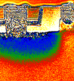
nFET junction map. Figure 4 shows the junction profile map for a n-type field effect transistor (nFET) by dual lens electron holography with (a) and (b) as the electrostatic potential and contour map, respectively, and (c) as the amplitude of electric field map calculated from the contour map by equations (5) and (6). The high intensity of the electric field along the sloped region in Figure 4(c) is consistent with the abrupt junction shown in the contour map in Figure 4(b) with dense contour lines at the same region. At the bottom of the source/drain region, because of slow change in the electric potential (shown in Figure 4(b) as less dense equal potential lines), the electric field in that region is relatively weak, as shown in Figure 4(c). The internal electric field under the gate is weaker relative to the sloped region.

Figure 5 is the result of a 4D-STEM experiment carried out on the nFET device to measure the electric field. The scan area is marked by a green box in Figure 5(a) to cover two contacts with a gate in the middle. Electric fields in the x and y directions measured using the method described above are displayed in Figures 5(b) and (c), respectively. Figure 5(d) is the amplitude of the internal electric field. The most significant feature in the electric field maps is that there are electric fields of opposite sign in the x direction between the left and right of the gate, and the same sign in the y direction on both sides of the gate. This can be understood by taking the derivative of the electrostatic potential measured by electron holography in Figure 4(a). Figure 4(c) shows the amplitude of the electron holography result calculated from the two measured components, Ex and Ey. The consistent maps obtained through these two techniques (Figures 4(c) and 5(d)) indicate that 4D-STEM experiments reconstruct the electric field information well. Based on the 2D electric field, we are also able to calculate the 2D charge density distribution using equation (7), with the charge density as of 1017 cm-3.

Figure 5: Electric field measurement on a nFET device by 4D STEM. (a) Overview of the sample, with the green box in the center indicating the area for 4D-STEM acquisition; (b) electric field maps measured by the 4D-STEM method along the x direction; (c) electric field along the y direction; (d) amplitude of the electric field. The red squares in (b), (c), and (d) indicate the gate location.
pFET junction map. Figure 6 shows an electrostatic potential map of a pFET device obtained by dual lens electron holography, with the vertical junction line near the gate (horizontal P-N junction direction) and an almost horizontal junction line (vertical P-N junction direction) at the bottom of the source drain region. Figure 6(a) is the original phase map from dual lens electron holography. Figure 6(b) is the contour map of Figure 6(a), and Figure 6(c) is the electric field profile calculated from Figure 6(b). Higher electric field near the gate is observed in Figure 6(c), which is consistent with dense contour lines in that region. Low electric field under the contact in the source/drain region is consistent with the less dense contour line in that region.

Figure 6: (a) pFET electrostatic potential map by dual lens electron holography; (b) contour map of electrostatic potential; (c) electric field of P-N junction from the contour map.
The same 4D STEM method was applied to measure the internal electric field of a PFET device (Figure 7). Figure 7(a) shows the STEM image of the scanned region as a green box and sample drift corrected region as a blue box. The electric field in the x and y directions (Figures 7(b) and (c)) clearly captures the feature of the derivative of the electrostatic potential measured in electron holography (Figure 6). The direction of the P-N junction boundary near the gate is almost vertical, as shown in Figure 6, and its electric field is in a horizontal direction illustrating the high electric field of Ex and almost zero electric field of Ey near the gate (Figure 7(b) and (c), respectively). Likewise, the direction of the P-N junction boundary at the bottom of the source/drain region is almost horizontal, which leads to a high electric field of Ey (vertical direction), but almost zero electric field of E x (Figures 7(c) and (b), respectively). In terms of direction of electric field, Ex has an opposite sign between the left and right of the gate, and the sign for Ey is the same between the left and right of the gate.

Figure 7: (a) Image of 4D STEM scanned region shown in the green box; (b) electric field along the x direction; (c) electric field along the y direction; (d) amplitude of the electric field. The red squares in (b), (c), and (d) indicate the gate location.
Discussion
Compared with electron holography, the 4D STEM method measures electron beam deflection through an electric field. Although the deflection of the electron beam is rather small, through data fitting one can directly measure the electric field. Compared with the DPC method, the advantage of this method is that it does not require complicated calibration, and data interpretation is straightforward. In addition, there is no extra hardware required for the measurement, while the DPC method requires 4 expensive segmented electron detectors.
In the measurements performed here, we tilted the sample slightly off-axis to avoid diffraction contrast in the main beam. The question is whether we can use the precession of the electron beam to average diffraction contrast while still being able to measure the electric field deflection of the electron beam. Since deflection of the electron beam is small and in the µrad range (approximately103–104 order smaller than the precession of the electron beam (3–20 mrad)), the precession could smear out the beam deflection, which makes the beam deflection measurement unfeasible.
In these measurements, we used a 0.3 mrad converging angle to get enough sensitivity in the beam deflection. Using Figure 4(g) from [Reference Hass10], the spot size of the probe is estimated to be ~5 nm. The high converging angle could reduce the beam spot, which would improve spatial resolution. However, with a higher converging angle beam, it was discovered by DPC measurements that sensitivity was decreased. One would expect a similar result if a high converging angle is used since the principle of the measurement is the same, except the detection method is different between the 4D STEM and DPC methods. Nevertheless, there may still be room for improvement with this technique.
Based on equation (2), another way to increase sensitivity is to reduce the electron beam energy to increase the deflection angle. For example, using a 100 keV electron beam to measure the beam deflection instead of regular 200 keV electron beam will reduce the velocity of the electron beam by half, leading to a 2× electron beam deflection with the same intensity on the internal electric field.
From the map comparison between 4D STEM and holography, electron holography seems to have better spatial resolution and a higher S/N ratio at this stage of development. Yet, 4D STEM may have potential in other applications, such as measurement of a dipole electric field or the internal electric field of a hetero-junction, where electrostatic potential measurement has both the material components (such as different electrostatic potential for Si and SiGe) and electric field from a P-N junction [Reference Wang1].
The measurement of electron beam deflection indicates the electric field strength of nFET is 3× higher than the one for pFET. The intensity of the internal electric field depends on the junction width and dopant concentration. This affects device performance and reliability, which may relate to the threshold of voltage breakdown for semiconductor devices.
It is noted that intensity of the electric field with scan direction from P to N is weaker than the one from N to P (Figure 7(d)). This may be attributed to the electron, which carries a negative charge that will cause a slight shift in electrostatic potential if the charge does not dissipate fast enough during the scan through the thin carbon layer coated on both sides of the sample.
Conclusion
In conclusion, a method of 4D STEM to measure the electric field of a P-N junction is reported and electric field maps of a semiconductor device compare favorably with the ones obtained by dual lens electron holography. Both methods measure the junction profile through different angles. One measures internal electric field of a P-N junction, and the other measures electrostatic potential. Compared with DPC methods, this method does not require extensive calibration and additional expansive hardware installation.
Acknowledgement
We would like to acknowledge skillful sample preparation by Xay Saythavy and stimulating discussion of junction profiling and TCAD simulation with Jochonia Nxumalo, Haitao Liu, Chandra Mouli, and Dan Mocuta.


