Hostname: page-component-848d4c4894-p2v8j Total loading time: 0.001 Render date: 2024-06-01T10:04:44.094Z Has data issue: false hasContentIssue false

Fabrication of p-β-Fe1−x Mnx Si2/n-Si Heterostructure Diode and their Electrical and Optical Properties

Published online by Cambridge University Press:  15 February 2011

T. Takada
Affiliation:
Electrotechnical Laboratory, 1–1–4 Umezono, Tsukuba, Tbaraki 305, Japan. Meiji University, 1–1–1 Higashi-mita, Tama, Kawasaki, Kanagawa 214, Japan
H. Katsumata
Affiliation:
Electrotechnical Laboratory, 1–1–4 Umezono, Tsukuba, Tbaraki 305, Japan. Meiji University, 1–1–1 Higashi-mita, Tama, Kawasaki, Kanagawa 214, Japan
Y. Makita
Affiliation:
Electrotechnical Laboratory, 1–1–4 Umezono, Tsukuba, Tbaraki 305, Japan.
N. Kobayashi
Affiliation:
Electrotechnical Laboratory, 1–1–4 Umezono, Tsukuba, Tbaraki 305, Japan.
M. Hasegawa
Affiliation:
Electrotechnical Laboratory, 1–1–4 Umezono, Tsukuba, Tbaraki 305, Japan.
S. Uekus
Affiliation:
Meiji University, 1–1–1 Higashi-mita, Tama, Kawasaki, Kanagawa 214, Japan
Get access

Abstract

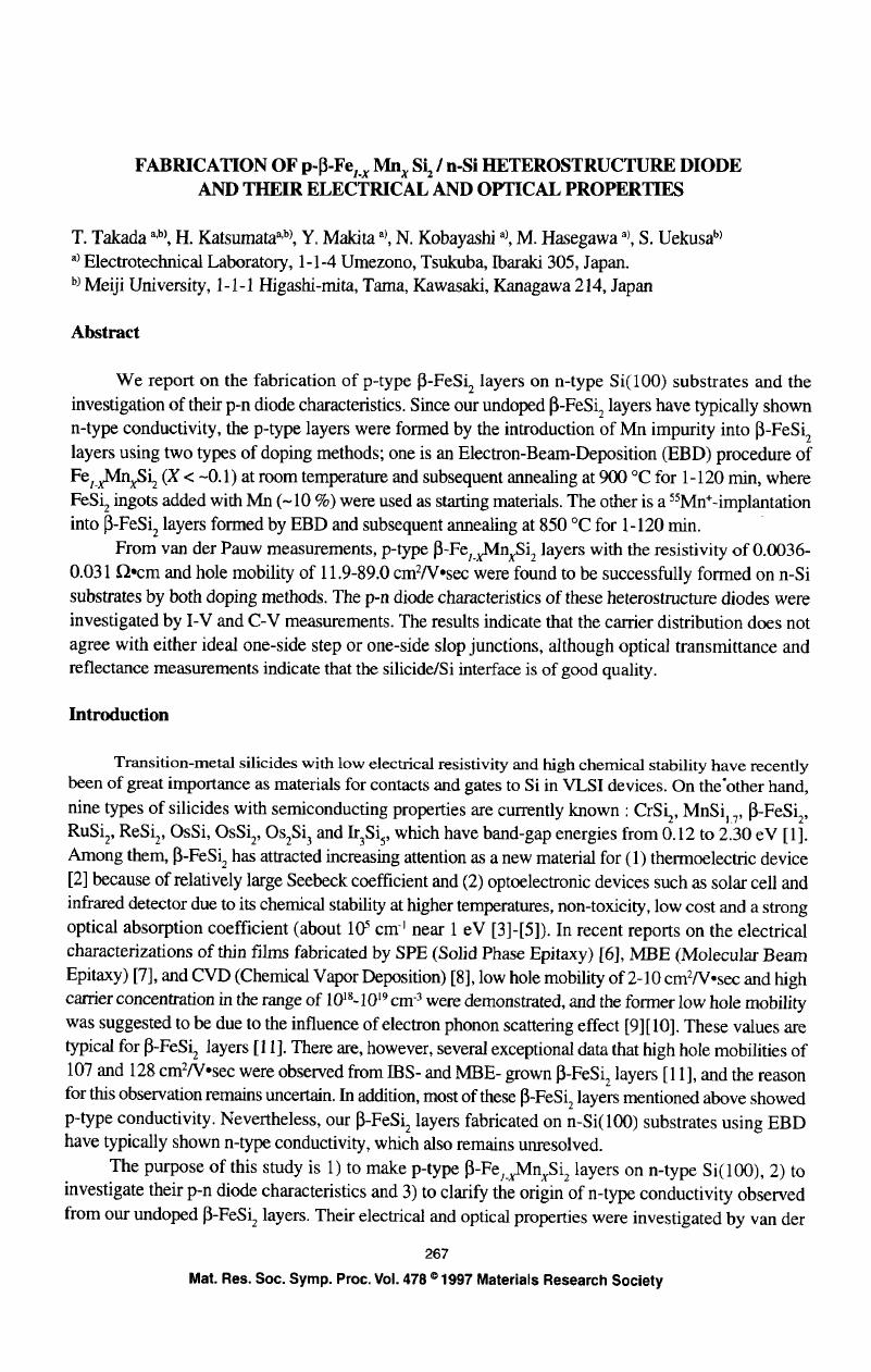
Image of the first page of this content. For PDF version, please use the ‘Save PDF’ preceeding this image.'
Type
Research Article
Copyright
Copyright © Materials Research Society 1997

Access options

Get access to the full version of this content by using one of the access options below. (Log in options will check for institutional or personal access. Content may require purchase if you do not have access.)

References

[1] Lange, H., Mat. Res. Soc. Symp. Proc. 402 (1996) 307.Google Scholar
[2] Tsunoda, T., Mukaida, M., Watanabe, A., Imai, Y., J. Mater. Res. 11 (1996) 1.Google Scholar
[3] Katsumata, H., Shen, H.L., Kobayashi, N., Makita, Y., Hasegawa, M., Shibata, H., Kimura, S., Obara, A., and Uekusa, S., Proc. of the 9th Int. Conf. on Ion Beam Modification of Materials, (1995) 943.Google Scholar
[4] Katsumata, H., Makita, Y., Shibata, H., Kobayashi, N., Hasegawa, M., Kimura, S., Obara, A., Contributed paper to XV INTERNATIONAL CONFERENCE ON THERMOELECTRICS (Pasadena, Calfolnia, USA).Google Scholar
[5] Kobayashi, N., Katsumata, H., Shen, H.L., Hasegawa, M., Makita, Y., Shibata, H., Kimura, S., Obara, A., and Uekusa, S., and Hatano, T., Thin Solid Films 270 (1995) 406.Google Scholar
[6] Nishida, I., Phys. Rev. B 7 (1973) 2710.Google Scholar
[7] Rizzi, A., Rosen, B.N.E., Freundt, D., Dieker, Ch. and Luth, H., Phys. Rev. B 51, (1995) 17780.Google Scholar
[8] Regolini, J. L., Tricat, F., Sagnes, I., Shapira, Y., Bremond, G., and Bensahel, D., IEEE Trans. Electron Devices 39 (1992) 200.Google Scholar
[9] Christensen, N. E., Phys. Rev. B 42 (1990) 7148.Google Scholar
[10] Giannini, C., Lagomarsino, S., Scarinci, F., and Castrucci, P., Phys, Rev. B 45 (1992) 8822.Google Scholar
[11] Radermacher, K., Carius, R. and Mantl, S., Nucl. Instr. & Meth. B 84 (1994) 163.Google Scholar
[12] Bost, M.C. and Mahan, John E., J. Appl. Phys. 64 (1988) 2034.Google Scholar