


1. Introduction
A multi-input, wide-band, and high-speed FPGA-based digital receiver described as the digital correlation receiver in this paper is developed and implemented for a new generation solar radio-interferometric synthetic telescope: Mingantu Spectral Radioheliograph (MUSER). MUSER is a solar-dedicated radio-interferometric array for imaging spectroscopy of the Sun in centimetric–decimetric wave range (Yan et al. 2012), which is capable of producing high spatial resolution, high temporal resolution, and high frequency resolution simultaneously. The MUSER array telescope is located within the radio-quiet zone around the Mingantu Observing Station in Inner-Mongolia in North China, currently consisting of 100 dish antennas totally. Forty 4.5-m antennas operate between 0.4 and 2 GHz, with the rest 60 2-m antennas operating between 2 and 15 GHz.
The whole 0.4–15 GHz radio-frequency (RF) band is divided into multiple sub-band with 400 MHz width and converted down to 50–450 MHz intermediate-frequency (IF) band. The task of the digital correlation receiver is to sample 50–450 MHz IF signals from all front ends of the MUSER array, channelise to split selected RF band, compute the correlation between all antenna baselines, and send out the correlation data stream for imaging.
There are some radioheliographs running for a long period before MUSER. The Nobeyama Radioheliograph (NoRH) consists of 84 antennas observing at 17 and 34 GHz (Nakajima et al. Reference Nakajima, Nishio, Enome, Shibasaki, Takano and Hanaoka1995). The Nancay Radioheliograph (NRH) has 47 antennas allowing simultaneous observations of up to 10 frequencies in the range of 150–450 MHz (Kerdraon & Delouis Reference Kerdraon and Delouis1997). The Siberian Solar Radio Telescope (SSRT; Grechnev et al. Reference Grechnev2003) consists of 256 antennas observing at 5.7 GHz only. The Gauribidanur Radioheliograph (Ramesh et al. Reference Ramesh, Subramanian, Sundararajan and Sastry1998) has 32 antenna groups composed by log periodic dipoles and operates at one single frequency in the range of 40–150 MHz. The Expanded Owens Valley Solar Array (EOVSA) is expanded as the prototype of the Frequency Agile Solar Radio Telescope (FASR; Bastian Reference Bastian2003), which has the similar imaging capability with MUSER. Up to now the EOVSA is operating in the frequency range of 2.5–18 GHz, but only consisting of a total 15 antennas so far (Gary et al. Reference Gary, Hurford, Nita, White, McTiernan and Fleishman2014). It seems that no existing radioheliograph is dealing with wide-band signal processing over a large amount of receiving elements. Thus the development of the MUSER digital-correlation-receiver has no ready-to-use solutions to implement crucial functions such as sampling synchronously between all receiving channels, channelising wide-band signals, and parallelising and pipelining high-speed real-time data streams. These issues led us to develop a dedicated FPGA-based digital receiver for the digital processing for the MUSER array.
In this paper, we firstly introduce the MUSER subsystems and the signal flow in the MUSER array. Then we present the MUSER digital-correlation-receiver architecture and explain the digital signal-processing process of the digital correlation receiver. We also discuss the hardware implementation thoroughly. In the end of the paper, we review the highlights in the digital-receiver design as well as explaining the importance of the MUSER digital correlation receiver to the new upcoming solar radio telescopes at the Mingantu observing station.
2. System overview
An overview of MUSER subsystems and connections is shown in Figure 1. The antennas of MUSER array are 100 dual-circle polarised dishes, arranged along three spiral arms and distributed in
 ${\sim}3$
-km radius area (Yan et al. 2012). The MUSER array is divided into two subarrays in different observing frequencies. MUSER IF array (MUSER-I) receives solar radio signals in 0.4–2 GHz and MUSER high-frequency (MUSER-H) array works in 2–15 GHz. Each antenna in both subarrays is equipped with an Left/Right (L/R) circle polarisation switch allowing a selected left-circle-polarised (LCP) or right-circle-polarised (RCP) solar radio signal amplified by the front-end amplifier and then transmitted to the analog receiver at MUSER central building through the underground optical fibre cables.
${\sim}3$
-km radius area (Yan et al. 2012). The MUSER array is divided into two subarrays in different observing frequencies. MUSER IF array (MUSER-I) receives solar radio signals in 0.4–2 GHz and MUSER high-frequency (MUSER-H) array works in 2–15 GHz. Each antenna in both subarrays is equipped with an Left/Right (L/R) circle polarisation switch allowing a selected left-circle-polarised (LCP) or right-circle-polarised (RCP) solar radio signal amplified by the front-end amplifier and then transmitted to the analog receiver at MUSER central building through the underground optical fibre cables.
Figure 1. An overview of MUSER subsystems and connections.
The MUSER receiver unit (the case of MUSER-I is shown in Figure 2) contains the analog and digital signal processing electronic hardware to receive and process all RF signals from each antenna front end. At each antenna front end, an ultra-wide band feed (MUSER-I: 0.4–2 GHz; MUSER-H: 2–15 GHz) collects the sky radio-band signal and forms LCP and RCP signals, which are selectable along with signals from the test port and noise source by a 4-to-1 switch. Then an electric-optical transmitter modulates and transmits the amplified radio signals into the in-door receiving unit via the underground fibre cables. The analog receiver transforms the received optical signals into electric-voltage signals, converting the wide-band RF signals down to multiple IF bands with band-limiting filters. The total amplification is 68 dB and adjustable in a 30 dB range via step attenuators with a resolution of 1 dB. A band-limited signal-band with a 3 dB bandpass between 50 and 450 MHz and a stop-band attenuation better than 30 dB at 450 MHz is passed on to the digital correlation receiver.
Figure 2. A schematic view of MUSER-I receiver unit.
The specifications of the digital correlation receiver are given in Table 1. Inside the digital correlation receiver, all IF signals from each antenna are continuously sampled with 1 GHz clock, quantised with 10 bits, and channelised to form the baseband signals. (Bandwidth is adjustable from 25 to 1.5625 MHz. The sixteen 25 MHz bandwidth signals compose the full 400 MHz IF bandwidth. In other cases, such as 12.5 MHz bandwidth, there are gaps between two adjacent 12.5 MHz bandwidth signals.) And the baseband signals are correlated to produce the correlation output data which is transmitted via RocketIO ports and then received by an interim data storage server with
 ${\sim}140$
TB capacity through PCI-E bus. A data processing pipeline called MUSEROS fetches and pipelines the calibrated data, providing ‘dirty’ and ‘clean’ solar maps at different frequencies.
${\sim}140$
TB capacity through PCI-E bus. A data processing pipeline called MUSEROS fetches and pipelines the calibrated data, providing ‘dirty’ and ‘clean’ solar maps at different frequencies.
Table 1. The MUSER digital-correlation-receiver specifications.

To keep the whole phase stability in an acceptable range (
 $\pm5^\circ$
), an temperature-control box is deployed to accommodate each front-end unit, providing the constant local environment temperature in the case of extreme weather. An underground optical fibre cable network is also used on Mingantu Observing Station (MOS) site to carry the RF signals, timing signals, and status signals of front-end units. All optical fibre cables extend from each antenna to MOS central building by the same length of 3 km, which is equal to the max distance of MUSER array range.
$\pm5^\circ$
), an temperature-control box is deployed to accommodate each front-end unit, providing the constant local environment temperature in the case of extreme weather. An underground optical fibre cable network is also used on Mingantu Observing Station (MOS) site to carry the RF signals, timing signals, and status signals of front-end units. All optical fibre cables extend from each antenna to MOS central building by the same length of 3 km, which is equal to the max distance of MUSER array range.
3. Design of the digital correlation receiver
3.1. Architecture
An overview of the digital signal-processing design is shown in Figure 3. Inside MUSER-I and MUSER-H digital correlation receiver, there are 44 and 64 receiving paths individually. The four additional receiving paths are reserved for the possible extending in the future. We present the design principles and implementation of MUSER-I digital correlation receiver in the rest sections since both MUSER-I and MUSER-H digital receiver share the very same signal-processing architecture. Each of receiving paths in the digital receiver contains analog-to-digital converter (ADC), delay-chain, polyphase filter channeliser (PFC), cascade half-band-filter chain, 2-bit requantiser. All paths end in the complex-correlation block which consists of multiple correlation units with each composed by one complex multiplier and one accumulator.
Figure 3. An overview of the signal-processing architecture in MUSER digital correlation receiver, with only one correlation block (including multiple correlation units) shown for a quick view.
The ADCs work at a 1 GHz sampling clock rate and quantise the 400-MHz bandwidth IF inputs into a 10-bit data sequences, which are bounded by the Nyquist frequency 500 MHz. The ADC outputs enter into the PFC module after passing through a delay register chain. The PFC module channelises the total 500 MHz into 20 channels with each having 25 MHz bandwidth. As the processed IF bands are from 50 to 450 MHz, 16 channels (except for the 1st, 2nd, 19th, and 20th) will be regrouped and sent into the next stage. The data of 16 channels are further quantised to real and imaginary pairs by the 2-bit requantiser and the quantised data enter into the complex correlation unit along with other 2-bit quantised data from different antennas. The correlation output from the averager in the complex correlation are packetised and aggregated, lined into the RocketIO ports and transmitted through optical fibres onto the storage server. The storage server uses PCI-E as the receiving port of correlation data and other aggregated data including power data, GPS time label, and system information.
The digital correlation receiver measures the signal power of each channel of PFC from all antennas as well as the cross-correlation from each baseline. The bandwidth of each channel can be selected from a range of multiple half-times of 25 MHz (see Sections 3.2.2 and 3.4). Delay tracking and phase tracking can also be turned on or off at the requests of various observations (Section 3.4).
3.2. Signal processing
3.2.1. ADC sampling
In most cases of solar radio observations, the signal power of solar radio bursts is much stronger than the quiet sun, in a degree of several tens of decibels. Any radio-frequency interference (RFI) in the observing bands also has a heavy effect on the ADC inputs. As a result, the amplitude of the signal power at the ADC inputs should be set to an optimal level for efficient use of the dynamic range of ADCs. The ADCs have 10-bit quantised levels. At 1 GHz sampling clock, the Effective number of bits (ENOB) is
 ${\sim}7$
bits, so the dynamic range of ADCs is
${\sim}7$
bits, so the dynamic range of ADCs is
 ${\sim}42$
dB. The monitor of power of the ADC’s input from a specified antenna can tell if the signal power is too strong to be clipped during ADC sampling when the antenna array tracking the sun. The adjustable step attenuators at the analog receiver’s outputs need to be changed in monitor and control software manually when signal power saturation happens such as extreme intense solar radio bursts.
${\sim}42$
dB. The monitor of power of the ADC’s input from a specified antenna can tell if the signal power is too strong to be clipped during ADC sampling when the antenna array tracking the sun. The adjustable step attenuators at the analog receiver’s outputs need to be changed in monitor and control software manually when signal power saturation happens such as extreme intense solar radio bursts.
3.2.2. Polyphase filter channeliser
The MUSER digital correlation receiver uses the PFC described in Lou, Xu, & Yang (Reference Lou, Xu and Yang2001) and Harris, Dick, & Rice (Reference Harris, Dick and Rice2003) to divide the 500 MHz wide band into 16 channels of 25 MHz bandwidth. A widely used channeliser in FX-correlators (Chikada et al. Reference Chikada1986) is the ‘polyphase filter bank’ (PFB; Harris & Haines Reference Harris and Haines2011). Since PFC and PFB have similar structure, they are both efficient methods to channelise wide-band signals (computational requirements are discussed in Appendix A). In MUSER, the zero-delay cross-correlation functions in time domain are measured for all antenna baselines, which can be achieved with PFC. Appendix A gives a short introduction of the PFC principle and implementation. The PFC employs a different channel-splitting process (Figure 4) compared with the usual channel-splitting method. The 20-channel PFC implementation is represented in Figure 5.
Figure 4. An alternate digital band-splitting method in the PFC with a real wide-band signal input. Note that each output has in-phase and quadrature components (real and imaginary). Complex conjugation should be applied to band-limited signals with negative frequency components to get the appropriate phases.

Figure 5. The structure of PFC with real input.
A prototype low-pass filter’s response is shown in Figure 6. The passband cut-off frequency is 20 MHz and the stopband cut-off frequency is 25 MHz. The ripple in passband is less than 0.5 dB and the attenuation of stopband is 60 dB. When using equal-ripple design method, such a specification requires a 440-point length for optimal implementation. Thus in each polyphase branch of PFC, the number of an individual polyphase filter’s taps is 22.
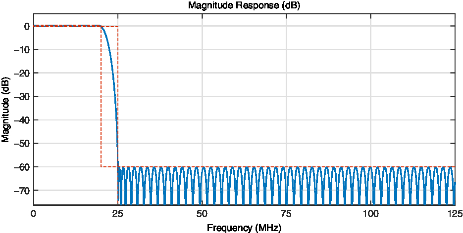
Figure 6. The prototype low-pass filter design.
3.2.3. Delay and phase tracking
In the MUSER digital correlation receiver, the digital delay is employed to compensate the geometric delay variation when all antennas tracking the Sun. The geometric delay is compensated through adjusting the shift-register chain at 1 GHz sampling clock before sampled signals entering into the PFC. In practice, there is a specified reference antenna acted as zero-delay centre and the 1-ns-step varying delays are applied to other antennas. Because the geometric delay changes continuously during observation while the digital delay applied to each antenna is discrete, the error between
 $\tau_g$
(geometric delay) and
$\tau_g$
(geometric delay) and
 $\tau_d$
(digital delay) will produce phase error on the edge of the bandwidth and give rise to the loss of the correlation amplitude. For MUSER, the estimated loss of the correlation amplitude due to the limited bandwidth and delay error is
$\tau_d$
(digital delay) will produce phase error on the edge of the bandwidth and give rise to the loss of the correlation amplitude. For MUSER, the estimated loss of the correlation amplitude due to the limited bandwidth and delay error is
 ${\sim} 0.07\%$
(see Appendix B).
${\sim} 0.07\%$
(see Appendix B).
The computed geometric delay can be split into integer part and fractional part. The fractional delay parts are converted into the phase corresponding to each central frequency of the PFC’s output and applied into all 16 frequency channels along with the phase tracking for convenience (see Figure 7). The accuracy of each baseline’s geometric delay computing depends on the accuracy of the Sun’s pointing angle. The solar position algorithm (Meeus Reference Meeus1991) we used can compute the solar zenith and azimuth angles in the period from the year 2000 BCE to 6000 CE with uncertainties of
 $\pm{0.0003^\circ}$
.
$\pm{0.0003^\circ}$
.

Figure 7. Delay and phase tracking.
3.2.4. A 2-bit requantiser
We employ a 2-bit requantiser in the MUSER digital correlation receiver, which is mainly based on two reasons. Firstly, the data processing capability of hardware was very limited during the period of MUSER’s first four years (2010–2013). In the case of MUSER-I, there is no enough digital signal processing (DSP) resources to handle band channelisation and correlation in data acquisition (DAQ) boards concurrently. Thus, all data of baseband channels for each antenna have to be sent to correlation (COR) boards with data buses on the backplane. Assuming the output bit length is 18 bit for one channel, the total data bandwidth is
 $$18 b \times 40\,(\mathrm{Ant.}) \times 16\,(\mathrm{Ch.}) \times 50 \,\mathrm{Ms}^{-1}=72\, \mathrm{GBs}^{-1}.$$
When using 2-bit quantisation, the total data bandwidth is reduced by
 ${\sim} 10$
times with which the backplane is able to transmit. In addition, 2-bit quantisation has sufficient sensitivity compared to 1-bit quantisation strategy used by both NoRH and NRH. Here is a quick look of the sensitivity difference between 1-bit and 2-bit quantisation (see Table 2).
${\sim} 10$
times with which the backplane is able to transmit. In addition, 2-bit quantisation has sufficient sensitivity compared to 1-bit quantisation strategy used by both NoRH and NRH. Here is a quick look of the sensitivity difference between 1-bit and 2-bit quantisation (see Table 2).
Table 2. The relative sensitivity of 1-bit and 2-bit quantisation.

 $\eta_Q$
is the relative sensitivity compared with the sensitivity without quantisation, and
$\eta_Q$
is the relative sensitivity compared with the sensitivity without quantisation, and
 $\beta$
is the multiples of Nyquist sampling rate. We see that the sensitivity is increased by 20% from 1-bit quantisation to 2-bit quantisation (see more details in Appendix C). Each output of the PFC module is quantised to 2-bit real and 2-bit imaginary pairs for the correlation computing. One method is to compute the mean value and the RMS value of PFC’s outputs such that they could be used as thresholds for requantising multiple-bit data (Thompson, Moran, & Swenson Reference Thompson, Moran and Swenson2001). Another requantising method is to use saturating and rounding logic to truncate the 18-bit data from PFC’s outputs into 2-bit representation. Both methods have been implemented in the MUSER digital correlation receiver, and the correlation phase results of two methods show imperceptible changes. Hence, the saturating and rounding method is actually used for the 2-bit requantiser of the MUSER digital correlation receiver.
$\beta$
is the multiples of Nyquist sampling rate. We see that the sensitivity is increased by 20% from 1-bit quantisation to 2-bit quantisation (see more details in Appendix C). Each output of the PFC module is quantised to 2-bit real and 2-bit imaginary pairs for the correlation computing. One method is to compute the mean value and the RMS value of PFC’s outputs such that they could be used as thresholds for requantising multiple-bit data (Thompson, Moran, & Swenson Reference Thompson, Moran and Swenson2001). Another requantising method is to use saturating and rounding logic to truncate the 18-bit data from PFC’s outputs into 2-bit representation. Both methods have been implemented in the MUSER digital correlation receiver, and the correlation phase results of two methods show imperceptible changes. Hence, the saturating and rounding method is actually used for the 2-bit requantiser of the MUSER digital correlation receiver.
3.3. Data streams and interfaces
The output of the MUSER digital correlation receiver consisting of both cross-correlation data of all 16 channels over 400 MHz wide IF band from all baselines and power data of all frequency channels from all antennas is continuously stored in an interim storage server with a self-defined file format. Each raw-data file includes 19 200 frames and each frame is of
 ${\sim}100$
KB for MUSER-I and of
${\sim}100$
KB for MUSER-I and of
 ${\sim}200$
KB for MUSER-H. A data frame is formed by
${\sim}200$
KB for MUSER-H. A data frame is formed by
 ${\sim}3$
ms integration and includes GPS timestamps, observation parameters such as RF band tags, RCP/LCP tags, and bandwidth, in its header along with the data segment.
${\sim}3$
ms integration and includes GPS timestamps, observation parameters such as RF band tags, RCP/LCP tags, and bandwidth, in its header along with the data segment.
The storage server runs with a redundant array of independent disks (RAID) storage (44TB) hard-disk array (44 TB for MUSER-I and 100 TB for MUSER-H). After calibrating, the MUSEROS program reads the raw-data files and converts them into flexible image transport system (FITS) format files to be further parsed and processed either by imaging modules embedded in the MUSEROS or by external imaging programs such like Common Astronomy Software Applications (CASA).
The raw data stream of the digital correlator is sent out via RocketIO through optical fibres and received at the storage server via PCI-E x8 lanes. The data bandwidth of MUSER raw data streams is
 ${\sim}30$
MB/s for MUSER-I and
${\sim}30$
MB/s for MUSER-I and
 ${\sim}60$
MB/s for MUSER-H. The delay and phase tracking data are pre-computed on the workstation and then transmitted to the digital correlator via RocketIO through optical fibres. All control instructions and status data are sent and fetched via RS-422 provided by an Ethernet-RS server, which mounts various RS-422 ports onto virtual Ethernet ports. Thus, all devices can be controlled by a control computer from local area network (LAN).
${\sim}60$
MB/s for MUSER-H. The delay and phase tracking data are pre-computed on the workstation and then transmitted to the digital correlator via RocketIO through optical fibres. All control instructions and status data are sent and fetched via RS-422 provided by an Ethernet-RS server, which mounts various RS-422 ports onto virtual Ethernet ports. Thus, all devices can be controlled by a control computer from local area network (LAN).
3.4. Operation
A typical operation sequence of the digital correlation receiver is listed as the following:
1. Boot up the digital correlation receiver.
2. Set timing (default is traversing all RF sub-bands).
3. Automatically measure the delay difference among all sampling paths.
4. Set correlations parameters (delay and fringe switch, bandwidth, initial delays of all sampling paths).
5. Start data recording.
In the first step, the digital correlation receiver is initialised by loading the on-board FPGA firmware. Step 2 is optional and can be passed when running in the normal mode, which means the analog receiver periodically changes the frequency of locoal osscilators (LOs) so that the IF band is able to traverse all RF bands. Once the observation required finer temporal resolution, staying on a given RF band by setting timing in Step 2 would be helpful. Fixing or auto-switch RCP/LCP control signals are also configurable in Step 2. Inside Step 3, the digital correlation receiver will measure the delay differences, which occur randomly at the moment of boot-up, and compensate the delay differences. Operations in Step 4 allow us to switch delay and phase tracking on or off, change channels’ bandwidth, and apply initial delays onto all digital sampling paths simultaneously. The whole process is accomplished in the monitor & control software.
4. Implementation
4.1. Hardware implementation
4.1.1. Modules
The digital correlation receiver’s hardware modules for digital sampling and signal processing are implemented by three kinds of FPGA boards: DAQ board, COR board, and timing & data controller (TDC) board, which are shown in Figure 8.

Figure 8. An overview of the digital correlation receiver’s hardware architecture and modules.
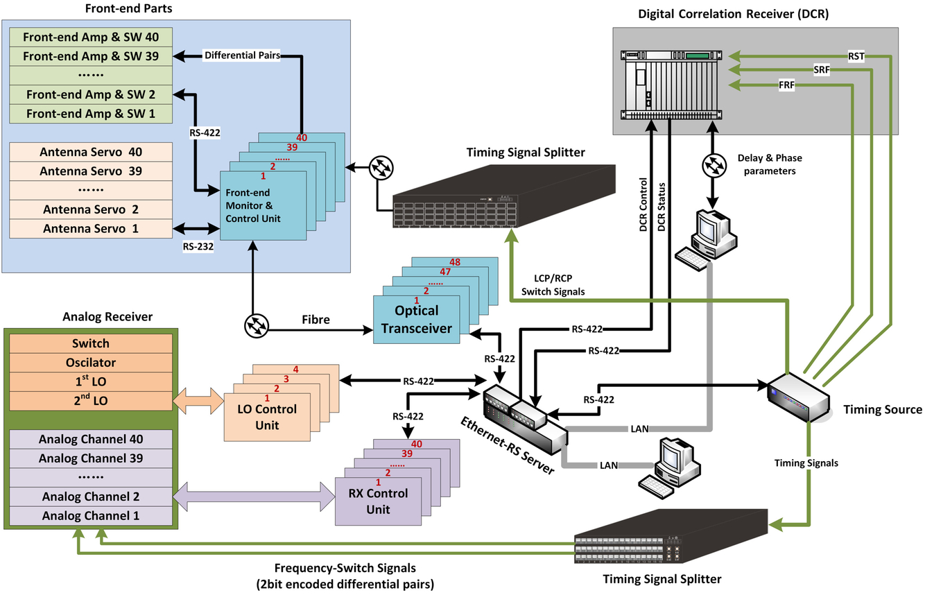
Figure 9. An overview of the monitor–control structure and interconnection.
The DAQ boards do the main signal processing including digital sampling and IF band channelisation. Digital sampling or analog-to-digital conversion is accomplished by e2v EV10AQ ADC, each of which consists of four sampling channels and runs at 1 GHz sampling clock per channel with 10-bit quantised length. The signal processing algrithms of eight digital inputs in each DAQ board, such as delay compensation, channelisation, phase tracking, and 2-bit requantisation, are implemented in Altera Stratix (S3 E260 for MUSER-I and S4 GX530 for MUSER-H) FPGAs. There are two e2v ADC chips and one Stratix FPGA on a single DAQ board, and the total number of DAQ boards are six for MUSER-I and eight for MUSER-H.
As for the correlation, there are four COR boards to receive and process all 2-bit quantised data from DAQ boards. The correlation computation mainly consists of complex multiplication and accumulation implemented in Altera Stratix FPGAs as same as used on DAQ boards. There are two Stratix FPGAs on each COR board.
The TDC board provides required timing signals to DAQ and COR boards and carries out the data aggregation for the output including packetising, data serialising, and electrical-to-optical fibre signal conversion. The logic management of data aggregator is implemented in a Xilinx Virtex-5 SX95 FPGA.
All of the module boards are integrated by a custom backplane board providing multiple plug-in VPX slots. The backplane board also contains high-speed signal paths allowing data exchanged and timing signals distributed between different boards.
4.1.2 Timing signals
The signal-processing pipeline in the digital correlation receiver is controlled by timing signals provided by the TDC board, which are originally from the timing source of the monitor–control unit. The timing source is shown in Figure 1, which receives an external reference clock at 10 MHz and PPS (pulse per second) from the GPS clock and generates a group of timing signals such as the full-radio-frequency pulse (FRF) and single-radio-frequency pulse (SRF) for both digital signal-processing pipelining and analog receiver’s LO switching.
The timing signal FRF plays a leading role in controlling signal-processing pipeline in the MUSER digital correlation receiver. The period of FRF is 25 ms for the full observation in 0.4–2 GHz, including four 400 MHz bandwidth jumping and two LCP/RCP switching. Some timing signals including SRF, RF switch, and LCP/RCP switch signals are derived from FRF and sent to all antenna front ends and indoor analog receivers to warrant that all sub-elements work in keeping with the specified timing.
The sampling clock and the FPGA processing clock are derived from the clock module. The clock module receives the same external reference clock at 10 MHz as the timing source receives from the GPS clock module, and then produces a phase-locked analog clock at 2 GHz, which is split and amplified to drive all ADCs’ sampling clocks. The 2 GHz analog clock’s rate is further divided and phase-locked to produce a processing clock at 250 MHz distributed to all FPGAs in boards.
4.2. Monitor and control
The monitor–control unit consists of two control computers, two timing signal splitter, a timing source and a Ethernet-RS server. Control instructions from control computers are transmitted to the timing source routed by the Ethernet-RS server via Ethernet, where the instructions are formatted and packetised and sent to in-door devices via RS-422. For the out-door front ends, optical transceivers bridge the RS-422 control signals to the far field through optical fibres. The monitor–control’s structure and interconnection are shown in Figure 9.
5. Discussion
Great volume of solar radio observations and researches indicate that a solar eruption always involves complex physical processes. For example, a solar flare may compose of thousands of radio bursts with very small time scales and complicated spectral fine structures, including spikes, dots, and narrow-band type III bursts. They are related to each single magnetic energy release process and can be regarded as the elementary bursts in solar eruptions (Tan Reference Tan2013). The scaling laws of the solar radio elementary bursts provide a basic requirement for the new solar radio telescopes. A typical estimation of the frequency resolution to recognise the elementary bursts is about 0.2–0.3% of the central frequency for the broadband radio spectrometers and 2–3% of the central frequency for the broadband radio heliographs. The temporal resolution depends on the frequencies; for example, the cadence is required to be less 10 ms in the broadband radio spectrometers and less 100 ms in the broadband radio heliographs, respectively (Tan et al. Reference Tan, Cheng, Tan and Kuo2018). For this purpose, the future enhanced MUSER digital correlation receiver should be capable of providing a power spectrum with a finer frequency resolution (
 ${\sim}1$
MHz in 0.4–2 GHz). Another purpose for enhancing the current digital correlation receiver is to recognise and excise the increasing RFI around the Mingantu Observing Station. The new jobs can be accomplished by implementation through the combination of FPGA-based hardware and GPU-based data pro-processing pipeline. With computing the spectral kurtosis (Nita & Gary Reference Nita and Gary2010) at each frequency bin produced from FPGA, the GPU-cased data pro-processing pipeline is able to discriminate between RFI-contaminated bins and normal bins. Thus, the RFI recognition and excision can be done with low effort.
${\sim}1$
MHz in 0.4–2 GHz). Another purpose for enhancing the current digital correlation receiver is to recognise and excise the increasing RFI around the Mingantu Observing Station. The new jobs can be accomplished by implementation through the combination of FPGA-based hardware and GPU-based data pro-processing pipeline. With computing the spectral kurtosis (Nita & Gary Reference Nita and Gary2010) at each frequency bin produced from FPGA, the GPU-cased data pro-processing pipeline is able to discriminate between RFI-contaminated bins and normal bins. Thus, the RFI recognition and excision can be done with low effort.
6. Summary
The MUSER digital correlation receiver employs high-speed analog-to-digital converters for sampling a wide IF band of 400 MHz and FPGA-based hardware for pipelining a heavy real-time signal-processing workload from a large number of antenna baselines. A PFC is implemented in the digital correlation receiver, which offers an alternative cost-effective method to accomplish wide-band signal channelisation besides PFB widely used in FX correlators. And the system design proves to be efficient when sampling and processing a large bandwidth of radio signals even now there are more advanced high performance ADCs and FPGAs off the shelf. More solar radio observing instruments such as MUSER decametric-metric array and IPS (interplanetary scintillation) telescope are in a construction list within the next few years. One important common feature between these instruments is that they all require a large amount of signal receiving front ends and moderate frequency channels. Therefore, the current MUSER digital correlation receiver appears to be a reference design to the digital-backend processing system both in the MUSER decametric-metric array and the IPS telescope.
Acknowledgements
Support for the MUSER comes from the National Major Scientific Research Facility Program of China with the grant number ZDYZ2009-3. We also acknowledge the support provided by the NFSC grant numbers 11433006, 11573043, 11790301, 11773043, and 11790305.
Appendix A. An introduction of PFC
In this section, we introduce the PFC’s structure with an example that the input signal is split into four channels over the full band. We can obtain a general form of the PFC when the full band is divided with a specific method (alternate channel splitting).
We start from the usual channel-splitting case, which is shown in Figure A1. Note that all positive-frequency components’ centres are moved to the zero frequency after frequency shift by multiplying certain complex phasors. Hence, we obtain the complex baseband signal which can be further down-sampled by 2D factor. The process is represented in Figure A2.
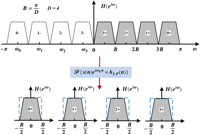
Figure A1. The usual channel-splitting method (D=4) of a real signal’s spectrum.
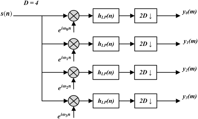
Figure A2. The canonical structure of the real-signal filter bank (D=4) with frequency shift and low-pass filter.
Figure A3. The alternate channel-splitting method (D=4) of a real signal’s spectrum.
The canonical structure of the real-signal filter bank with frequency shift and low-pass filter requires lots of DSP resources and is hard to implement in practice because (1) a high-order low-pass filter is applied for each branch in the structure which will consume much DSP resources and (2) the down-sampling function lies on the end of the branch so the previous high-speed input signal may exceed the DSP processing speed. Fortunately, there is an efficient implementation to overcome these disadvantages. Firstly, divide the full digital frequency band in the alternate way (shown in Figure A3). In this way, we use both positive-frequency and negative-frequency bands, and
 $\omega_{k}=\frac{\pi}{D} \cdot \left(2k+\frac{1}{2}-D\right), k=0,1, \dots , D-1$
.
$\omega_{k}=\frac{\pi}{D} \cdot \left(2k+\frac{1}{2}-D\right), k=0,1, \dots , D-1$
.
We can deduce the polyphase channeliser structure by starting from the expression of the canonical structure of the real-signal filter bank:
 \begin{align*}
y_{k}(m) &=\left.\left\{\left[s(n) \mathrm{e}^{\mathrm{i} \omega_{k} n}\right] * h(n)\right\}\right|_{n=m(2 D)} \\[2pt] &=\left.\left\{\sum_{i=-\infty}^{+\infty} s(n-i) \mathrm{e}^{\mathrm{i} \omega_{k}(n-i)} \cdot h(i)\right\}\right|_{n=m(2 D)} \\[2pt] &=\sum_{i=-\infty}^{+\infty} s(2 m D-i) \mathrm{e}^{\mathrm{i} \omega_{k}(2 m D-i)} \cdot h(i) \\[2pt] &=\sum_{p=0}^{D-1} \sum_{i=-\infty}^{+\infty} s(2 m D-i D-p) \mathrm{e}^{\mathrm{i} \omega_{k}(2 m D-i D-p)} \\[2pt] & \qquad\qquad\qquad \cdot h(i D+p) \\[2pt] &=\sum_{p=0}^{D-1} \sum_{i=-\infty}^{+\infty} s_{p}(2 m-i) \mathrm{e}^{\mathrm{i} \omega_{k}(2 m-i) D} \cdot h_{p}(i) \mathrm{e}^{-\mathrm{i} \omega_{k} p} \\[2pt] &=\sum_{p=0}^{D-1}\left\{\left[s_{p}(n) \mathrm{e}^{\mathrm{i} \omega_{k} n D}\right] * h_{p}(n)\right\}_{n=2 m} \cdot \mathrm{e}^{-\mathrm{i} \omega_{k} p}.
\end{align*}
\begin{align*}
y_{k}(m) &=\left.\left\{\left[s(n) \mathrm{e}^{\mathrm{i} \omega_{k} n}\right] * h(n)\right\}\right|_{n=m(2 D)} \\[2pt] &=\left.\left\{\sum_{i=-\infty}^{+\infty} s(n-i) \mathrm{e}^{\mathrm{i} \omega_{k}(n-i)} \cdot h(i)\right\}\right|_{n=m(2 D)} \\[2pt] &=\sum_{i=-\infty}^{+\infty} s(2 m D-i) \mathrm{e}^{\mathrm{i} \omega_{k}(2 m D-i)} \cdot h(i) \\[2pt] &=\sum_{p=0}^{D-1} \sum_{i=-\infty}^{+\infty} s(2 m D-i D-p) \mathrm{e}^{\mathrm{i} \omega_{k}(2 m D-i D-p)} \\[2pt] & \qquad\qquad\qquad \cdot h(i D+p) \\[2pt] &=\sum_{p=0}^{D-1} \sum_{i=-\infty}^{+\infty} s_{p}(2 m-i) \mathrm{e}^{\mathrm{i} \omega_{k}(2 m-i) D} \cdot h_{p}(i) \mathrm{e}^{-\mathrm{i} \omega_{k} p} \\[2pt] &=\sum_{p=0}^{D-1}\left\{\left[s_{p}(n) \mathrm{e}^{\mathrm{i} \omega_{k} n D}\right] * h_{p}(n)\right\}_{n=2 m} \cdot \mathrm{e}^{-\mathrm{i} \omega_{k} p}.
\end{align*}
Let
 $x_{p}(m)=\left[s_{p}(m) \mathrm{e}^{\mathrm{i} \omega_{k} m D}\right] * h_{p}(m)=s_{p}^{\prime}(m) * h_{p}(m)$
, and
$x_{p}(m)=\left[s_{p}(m) \mathrm{e}^{\mathrm{i} \omega_{k} m D}\right] * h_{p}(m)=s_{p}^{\prime}(m) * h_{p}(m)$
, and
 $s_{p}^{\prime}(m)=s_{p}(m) \mathrm{e}^{\mathrm{i} \omega_{k} m D}$
.
$s_{p}^{\prime}(m)=s_{p}(m) \mathrm{e}^{\mathrm{i} \omega_{k} m D}$
.
In this case:
 $\omega_{k}=\frac{\pi}{D} \cdot \left(2k+\frac{1}{2}-D\right)$
, so
$\omega_{k}=\frac{\pi}{D} \cdot \left(2k+\frac{1}{2}-D\right)$
, so
 $s_{p}^{\prime}(m)=s_{p}(m) \mathrm{e}^{\mathrm{i} \frac{\pi}{2} m }(-1)^{mD}$
.
$s_{p}^{\prime}(m)=s_{p}(m) \mathrm{e}^{\mathrm{i} \frac{\pi}{2} m }(-1)^{mD}$
.
Now we have
 $$\begin{equation*}
y_{k}(m)=\sum_{p=0}^{D-1} x_{p}(2 m) \mathrm{e}^{-\mathrm{i} \omega_{k} p}.
\end{equation*}$$
$$\begin{equation*}
y_{k}(m)=\sum_{p=0}^{D-1} x_{p}(2 m) \mathrm{e}^{-\mathrm{i} \omega_{k} p}.
\end{equation*}$$
Note that
 $\omega_{k}=\frac{\pi}{D} \cdot \left(2k+\frac{1}{2}-D\right)$
, and finally we get
$\omega_{k}=\frac{\pi}{D} \cdot \left(2k+\frac{1}{2}-D\right)$
, and finally we get
 $$\begin{equation*}
\begin{aligned} y_{k}(m) &=\sum_{p=0}^{D-1}\left[x_{p}(2 m) \cdot \mathrm{e}^{-\mathrm{i}\frac{\pi}{2D} p} \cdot (-1)^{p}\right] \mathrm{e}^{-\mathrm{i} \frac{2 \pi}{D} k p} \\[2pt] &=\sum_{p=0}^{D-1} x_{p}^{\prime}(2 m) \mathrm{e}^{-\mathrm{i} \frac{2 \pi}{D} k p}=\operatorname{DFT}\left[x_{p}^{\prime}(2 m)\right], \end{aligned}
\end{equation*}$$
$$\begin{equation*}
\begin{aligned} y_{k}(m) &=\sum_{p=0}^{D-1}\left[x_{p}(2 m) \cdot \mathrm{e}^{-\mathrm{i}\frac{\pi}{2D} p} \cdot (-1)^{p}\right] \mathrm{e}^{-\mathrm{i} \frac{2 \pi}{D} k p} \\[2pt] &=\sum_{p=0}^{D-1} x_{p}^{\prime}(2 m) \mathrm{e}^{-\mathrm{i} \frac{2 \pi}{D} k p}=\operatorname{DFT}\left[x_{p}^{\prime}(2 m)\right], \end{aligned}
\end{equation*}$$
where
 $x_{p}^{\prime}(2 m)=x_{p}(2 m) \cdot \mathrm{e}^{-\mathrm{i}\frac{\pi}{2D} p} \cdot (-1)^{p}$
.
$x_{p}^{\prime}(2 m)=x_{p}(2 m) \cdot \mathrm{e}^{-\mathrm{i}\frac{\pi}{2D} p} \cdot (-1)^{p}$
.
 $\mathrm{DFT}(\cdot)$
is discrete-Fourier-transform which can be implemented with FFT (Fast Fourier transform). The polyphase channeliser structure is represented in Figure A4.
$\mathrm{DFT}(\cdot)$
is discrete-Fourier-transform which can be implemented with FFT (Fast Fourier transform). The polyphase channeliser structure is represented in Figure A4.
The computational requirements of the PFB and the PFC can be compared by the real multiplications employed. For a D-channel spectrum channelisation, assuming the length of low-pass filter h(m) in PFC is
 $L_1$
, and the length of weighted window w(m) in PFB is
$L_1$
, and the length of weighted window w(m) in PFB is
 $L_2$
, there is a D-point FFT in PFC while a 2D-point FFT lies in PFB since a 2D-point FFT spectrum analyser returns D independent spectral channels for one real signal input. In general, the number of multipliers (real multiplications) of PFC and PFB can be estimated as follows:
$L_2$
, there is a D-point FFT in PFC while a 2D-point FFT lies in PFB since a 2D-point FFT spectrum analyser returns D independent spectral channels for one real signal input. In general, the number of multipliers (real multiplications) of PFC and PFB can be estimated as follows:
 \begin{gather*}
PFC\,:\, L_1+D+D+2D\cdot{{\rm log}_2{(D)}}=L_1+2D+2D\cdot{{\rm log}_2{(D),}}\\[5pt]
PFB\,:\, L_2+4D\cdot{{\rm log}_2{(2D)}}=L_2+4D+4D\cdot{{\rm log}_2{(D)}}.
\end{gather*}
\begin{gather*}
PFC\,:\, L_1+D+D+2D\cdot{{\rm log}_2{(D)}}=L_1+2D+2D\cdot{{\rm log}_2{(D),}}\\[5pt]
PFB\,:\, L_2+4D\cdot{{\rm log}_2{(2D)}}=L_2+4D+4D\cdot{{\rm log}_2{(D)}}.
\end{gather*}
In Harris & Haines (Reference Harris and Haines2011), the computational complexity of PFB is estimated as
 $\mathcal{O}(N(P+log(N))$
, where
$\mathcal{O}(N(P+log(N))$
, where
 $NP=L_2$
and
$NP=L_2$
and
 $N=2D$
in current context. In MUSER’s case, when
$N=2D$
in current context. In MUSER’s case, when
 $D=16$
and
$D=16$
and
 $L_1=L_2=440$
, the number of multipliers for a PFC from an antenna is
$L_1=L_2=440$
, the number of multipliers for a PFC from an antenna is
 ${\sim}600$
, while the number is
${\sim}600$
, while the number is
 ${\sim}760$
for a PFB from an antenna. Thus, in this case PFC requires less computational resource than PFB.
${\sim}760$
for a PFB from an antenna. Thus, in this case PFC requires less computational resource than PFB.
Appendix B. The analysis of bandwidth and delay-tracking error
If
 $\phi_m$
and
$\phi_m$
and
 $\phi_n$
are the phase errors for antenna m and antenna n, then
$\phi_n$
are the phase errors for antenna m and antenna n, then
 $\Delta\phi=\phi_m-\phi_n$
is the phase error. The correlator output can be expressed as (Thompson et al. Reference Thompson, Moran and Swenson2001):
$\Delta\phi=\phi_m-\phi_n$
is the phase error. The correlator output can be expressed as (Thompson et al. Reference Thompson, Moran and Swenson2001):

Figure A4. The polyphase channeliser structure with four channels (D=4).
 $$\begin{equation*}
r=V_{1} V_{2}^{*}[\langle\cos \Delta \phi+\sin \Delta \phi\rangle].
\end{equation*}$$
$$\begin{equation*}
r=V_{1} V_{2}^{*}[\langle\cos \Delta \phi+\sin \Delta \phi\rangle].
\end{equation*}$$
 $\Delta \phi=2 \pi \nu \Delta \tau$
,
$\Delta \phi=2 \pi \nu \Delta \tau$
,
 $\nu ({\rm frequency})$
varies from 0 to
$\nu ({\rm frequency})$
varies from 0 to
 $\Delta \nu ({\rm bandwidth})$
.
$\Delta \nu ({\rm bandwidth})$
.
 $\tau_s$
is the sampling interval in the digital receiver, which is applied to compensate
$\tau_s$
is the sampling interval in the digital receiver, which is applied to compensate
 $\tau_g$
. Let
$\tau_g$
. Let
 $\Delta \tau=\tau_{g}-\tau_{s}$
for single antenna, and we can reasonably assume that
$\Delta \tau=\tau_{g}-\tau_{s}$
for single antenna, and we can reasonably assume that
 $\Delta \tau$
is distributed uniformly in the interval
$\Delta \tau$
is distributed uniformly in the interval
 $\left[-\frac{\tau_{s}}{2}, \frac{\tau_{s}}{2}\right]$
. For any pair of antennas,
$\left[-\frac{\tau_{s}}{2}, \frac{\tau_{s}}{2}\right]$
. For any pair of antennas,
 $\Delta \tau_1$
and
$\Delta \tau_1$
and
 $\Delta \tau_2$
are independent so the combined delay error
$\Delta \tau_2$
are independent so the combined delay error
 $\Delta \tau$
has a triangular probability distribution between
$\Delta \tau$
has a triangular probability distribution between
 $\left[-\tau_{s}, \tau_{s}\right]$
, which gives
$\left[-\tau_{s}, \tau_{s}\right]$
, which gives
 $$\begin{equation*}
p(\Delta \tau)=\left(1-\frac{|\Delta \tau|}{\tau_{s}}\right) / \tau_{s}, \Delta \tau \in\left[-\tau_{s}, \tau_{s}\right].
\end{equation*}$$
$$\begin{equation*}
p(\Delta \tau)=\left(1-\frac{|\Delta \tau|}{\tau_{s}}\right) / \tau_{s}, \Delta \tau \in\left[-\tau_{s}, \tau_{s}\right].
\end{equation*}$$
We have known the output of the correlator is proportional to the cosine of the phase error. Thus, the response of the component at frequency \textit{v} equals~to
 $$\begin{equation*}
\begin{aligned}
&\int_{-\tau_{s}}^{\tau_{s}} p(\Delta \tau) \cos (2 \pi \nu \Delta \tau)\, {\rm d} \Delta \tau \\
={}& \frac{2}{\tau_{s}} \int_{0}^{\tau_{s}}\left(1-\frac{\Delta \tau}{\tau_{s}}\right) \cos (2 \pi \nu \Delta \tau)\, {\rm d} \Delta \tau \\
={}& \left[\frac{\sin \left(\pi \nu \tau_{s}\right)}{\pi \nu \tau_{s}}\right]^{2}.
\end{aligned}
\end{equation*}$$
$$\begin{equation*}
\begin{aligned}
&\int_{-\tau_{s}}^{\tau_{s}} p(\Delta \tau) \cos (2 \pi \nu \Delta \tau)\, {\rm d} \Delta \tau \\
={}& \frac{2}{\tau_{s}} \int_{0}^{\tau_{s}}\left(1-\frac{\Delta \tau}{\tau_{s}}\right) \cos (2 \pi \nu \Delta \tau)\, {\rm d} \Delta \tau \\
={}& \left[\frac{\sin \left(\pi \nu \tau_{s}\right)}{\pi \nu \tau_{s}}\right]^{2}.
\end{aligned}
\end{equation*}$$
For the bandwidth from 0 to
 $\Delta \nu$
, the response is
$\Delta \nu$
, the response is
 $$\begin{equation*}
\frac{1}{\Delta \nu} \int_{0}^{\Delta \nu}\left[\frac{\sin \left(\pi \nu \tau_{s}\right)}{\pi \nu \tau_{s}}\right]^{2} {\rm d} \nu=\frac{1}{\pi \Delta \nu \tau_{s}} \int_{0}^{\pi \Delta \nu \tau_{s}}\left[\frac{\sin t}{t}\right]^{2} {\rm d} t.
\end{equation*}$$
$$\begin{equation*}
\frac{1}{\Delta \nu} \int_{0}^{\Delta \nu}\left[\frac{\sin \left(\pi \nu \tau_{s}\right)}{\pi \nu \tau_{s}}\right]^{2} {\rm d} \nu=\frac{1}{\pi \Delta \nu \tau_{s}} \int_{0}^{\pi \Delta \nu \tau_{s}}\left[\frac{\sin t}{t}\right]^{2} {\rm d} t.
\end{equation*}$$
In the case of the MUSER digital correlation receiver,
 $\tau_{s}=1$
ns,
$\tau_{s}=1$
ns,
 $\Delta \nu=25$
MHz, and
$\Delta \nu=25$
MHz, and
 $\Delta \nu \tau_{s}=1 / 40$
, so the response can be calculated as
$\Delta \nu \tau_{s}=1 / 40$
, so the response can be calculated as
 $$\begin{equation*}
\frac{40}{\pi} \int_{0}^{\frac{\pi}{40}}\left[\frac{\sin t}{t}\right]^{2} {\rm d} t \cong 0.9993.
\end{equation*}$$
$$\begin{equation*}
\frac{40}{\pi} \int_{0}^{\frac{\pi}{40}}\left[\frac{\sin t}{t}\right]^{2} {\rm d} t \cong 0.9993.
\end{equation*}$$
That means only 0.07% loss in the sensitivity when the full 400 MHz band is channelised into 16 channels with 25 MHz bandwidth, which is acceptable in our case.
Appendix C. The analysis of 2-bit quantisation
Specifically, the sensitivity of 2-bit quantisation can be expressed as (Thompson et al. Reference Thompson, Moran and Swenson2001) follows:
 $$\begin{equation*}
\eta_{2 b}=\frac{R_{S N 2 b}}{R_{S N \infty}}=\frac{2[(n-1) E+1]^{2} \sqrt{\beta}}{\pi\left[\Phi+n^{2}(1-\Phi)\right] \sqrt{1+2 \sum_{q=1}^{\infty} R_{2 b}^{2}\left(q \tau_{s}\right)}}.
\end{equation*}$$
$$\begin{equation*}
\eta_{2 b}=\frac{R_{S N 2 b}}{R_{S N \infty}}=\frac{2[(n-1) E+1]^{2} \sqrt{\beta}}{\pi\left[\Phi+n^{2}(1-\Phi)\right] \sqrt{1+2 \sum_{q=1}^{\infty} R_{2 b}^{2}\left(q \tau_{s}\right)}}.
\end{equation*}$$
 $R_{S N 2 b}$
: The sensitivity of 2-bit quantisation.
$R_{S N 2 b}$
: The sensitivity of 2-bit quantisation.
 $R_{S N \infty}$
: The sensitivity of unquantisation.
$R_{S N \infty}$
: The sensitivity of unquantisation.
 $\beta$
: The multiples of Nyquist sampling rate.
$\beta$
: The multiples of Nyquist sampling rate.
 $\Phi$
: The probability when unquantised data are between
$\Phi$
: The probability when unquantised data are between
 $\pm v_{0}$
, and
$\pm v_{0}$
, and
 $v_{0}$
is the specified quantisation decision level.
$v_{0}$
is the specified quantisation decision level.
 $$\begin{equation*}
\Phi=\frac{1}{\delta \sqrt{2 \pi}} \int_{-v_{0}}^{v_{0}} \exp \left(-\frac{x^{2}}{2 \delta^{2}}\right) {\rm d} x=\operatorname{erf}\left(\frac{v_{0}}{\delta \sqrt{2}}\right),
\end{equation*}$$
$$\begin{equation*}
\Phi=\frac{1}{\delta \sqrt{2 \pi}} \int_{-v_{0}}^{v_{0}} \exp \left(-\frac{x^{2}}{2 \delta^{2}}\right) {\rm d} x=\operatorname{erf}\left(\frac{v_{0}}{\delta \sqrt{2}}\right),
\end{equation*}$$
 $$\begin{equation*}
E=\exp \left(-\frac{v_{0}^{2}}{2 \delta^{2}}\right),
\end{equation*}$$
$$\begin{equation*}
E=\exp \left(-\frac{v_{0}^{2}}{2 \delta^{2}}\right),
\end{equation*}$$
where
 $\delta$
is the RMS value of unquantised data.
$\delta$
is the RMS value of unquantised data.
 $$\begin{equation*}
\tau_{s}=(2 \beta \Delta \nu)^{-1},
\end{equation*}$$
$$\begin{equation*}
\tau_{s}=(2 \beta \Delta \nu)^{-1},
\end{equation*}$$
where
 $\Delta \nu$
is the bandwidth.
$\Delta \nu$
is the bandwidth.
We set
 $\beta = 1$
and
$\beta = 1$
and
 $v_{0}=\delta$
in our case, and the sensitivity is
$v_{0}=\delta$
in our case, and the sensitivity is
 $$\begin{equation*}
\eta_{2 b}=\frac{2\left[(n-1) e^{-1 / 2}+1\right]^{2}}{\pi\left[\operatorname{erf}(1 / \sqrt{2})+n^{2}(1-\operatorname{erf}(1 / \sqrt{2}))\right].}
\end{equation*}$$
$$\begin{equation*}
\eta_{2 b}=\frac{2\left[(n-1) e^{-1 / 2}+1\right]^{2}}{\pi\left[\operatorname{erf}(1 / \sqrt{2})+n^{2}(1-\operatorname{erf}(1 / \sqrt{2}))\right].}
\end{equation*}$$
Let
 $n=3$
, we see the sensitivity is
$n=3$
, we see the sensitivity is
 $\eta_{2 b}=0.881$
, as listed in Table 2.
$\eta_{2 b}=0.881$
, as listed in Table 2.


