Introduction
Recent improvements in material quality and contact technology for GaN-based materials system have led to a rapid progress in GaN devices. These devices include blue-green lasersReference Nakamura, Senoh, Nagahama, Iwasa, Yamada, Matsushita, Kiyoku and Sugimoto 1 , blue, green, and amber Light Emitting DiodesReference Nakamura, Mukai and Senoh 2 , Ultraviolet (UV) photodetectorsReference Razeghi and Rogalski 3 , Reference Shur and Khan 4 , and AlGaN/GaN Heterostructure Field Effect Transistors Reference Burm, Chu, Schaff, Eastman, Khan, Chen, Yang and Shur 5 - Reference Shur and Khan 11 . Wide band gap, high peak and saturation velocities, high breakdown voltage and chemical inertness make AlN-GaN-InN based semiconductors an excellent material for solar-blind optoelectronics, and high-power, hightemperature electronics.
GaN-based materials are usually grown in the [0001] direction (when they have the wurtzite crystal structure) and in the [111] direction (when they have the zinc blende crystal structure). These are polar axes, and, therefore, GaN-based materials exhibit strong lattice polarization effects. These effects are uniquely suited for applications in high temperature piezoelectronics and for applications in pyroelectric sensors.
We report on preliminary studies of pyroelectric properties of GaN. Much (if not most) of the work in this area remains to be done, and we expect dramatic improvements in GaN-based pyroelectric sensors still to come. We discuss the piezoelectric properties of III-Nitrides and the application of the concept of “piezoelectric doping” to GaN-based Heterostructure Field Effect Transistors. We consider the issue of spontaneous polarization in wurtzite GaN, AlN, and InN. Finally, we discuss several unresolved issues and make projections of future progress in GaNbased piezoelectronic devices.
Pyroelectricity in gallium nitride thin films
The pyroelectric materials are capable to generate an electric charge in response to heat flow. Heat sources affect the sample temperature by means of thermal convection, thermal diffusion or radiation. Both the primary pyroelectric effect and the secondary pyroelectric effect (piezoelectric effect caused by temperature induced strain) contribute to the pyroelectric response in GaN. The primary pyroelectric effect is dominant under the condition of a fast heat transfer. Such conditions can be implemented, for example, when the sensor is immersed in medium with a small viscosity and /or high flow velocity. In such moving medium (for example, hot gas flow), a GaN-based sensor will generate a voltage response, which is proportional to the heat flow (and, hence, to the gas flow).
Secondary pyroelectricity is linked to strain related to thermal expansion. For example, a difference in thermal expansion coefficients between a substrate and a pyroelectric film produces strain in response to temperature changes, which, in turn, generates an electric charge as a result of the piezoelectric effect.
Our estimates show that the sensitivity of GaN pyroelectric sensors can be significantly improved. The modeling results indicate that the pyroelectric voltage coefficients in GaN (for c-axis along the contacts) can be as high as 7×10⁵ V/m-K Reference Shur, Bykhovski, Gaska, Khan, Francombe and Wood 12 and exceed the P v = 5×10⁵ V/m-K for the best-known high temperature pyroelectric material LiTaO3 Reference Fraden 13 .
Therefore, GaN-based sensors should be suitable for high temperature pyroelectronics and piezoelectronics. Moreover, we expect that the pyroelectric effect will be more pronounced in insulating AlN or in AlGaN with a large Al mole fraction..
Low pressure MOCVD was used to fabricate all our samples (for the details of the growth procedure, see Reference Khan, Kuznia, Hove, Olson, Krishnankutty and Kolbas 14 ). The Hall electron concentration was approximately 5×10Reference Bayazitolu and Ozisik 16 cm−3 and the Hall mobility was on the order of 350 cm2/V-s. A typical sample resistance was close to 2 kΩ GaN layers, 3 − 5 μm thick, had ohmic contacts on the basal plane.
Pyroelectric properties of GaN were studied in two different regimes: (i) under applied temperature gradient along the sample and (ii) uniform sample heating.
The pyroelectric voltage was measured in the GaN sample subjected to uniform (see Fig. 1) and non-uniform (Fig. 2) heating and cooling.Reference Bykhovski, Kaminski, Shur, Chen and Khan 15 The time dependence of the voltage response in the GaN sample under applied temperature gradient is shown in Fig. 2. In these measurements, one contact was kept at a fixed temperature, which varied from 12 °C to 94 °C. The second contact was heated up to temperatures as high as 350 °C. The ambient temperature changed abruptly and a SmS-based thermoresistor monitored the sample temperature as a function of time. Cold and hot thermal shock experiments in the range from −100 °C to +300 °C used 96% ethyl or oil as a thermal bath. In these experiments, the heat transfer was caused mainly by free convection. Since the temperatures were relatively low, the radiative heat transfer was not important. Also, in uniform heating/cooling experiments, when the sample was dipped into the thermal bath, there was no appreciable temperature difference between the contacts, so that the sample did not act as a thermocouple.

Fig. 1. Pyroelectric voltage versus time for uniform heating and cooling (after Reference Bykhovski, Kaminski, Shur, Chen and Khan 15 ).

Fig. 2. Dynamics of contact temperature difference (a) and voltage response of GaN sample under non-uniform heating (b). Constant temperature of “cold” contact (94 °C) is shown by dotted line in Fig. 2a.
Due to a relatively high thermal conductivity of sapphire, the temperature gradients in the sample could be neglected under the uniform heating/cooling conditions, and the lumped system analysis was valid. Reference Bayazitolu and Ozisik 16 The pyroelectric effect in these experiments can be described by the heat transfer equation, the equation of motion of a viscous fluid, and the equation for pyroelectric polarization. Both the sample temperature change, T(t) - T(0), and the heat flow affect the polarization. The temperature change is proportional to the thermal energy stored or dissipated.
In Reference Reference Bykhovski, Kaminski, Shur, Chen and Khan 15 , we described a model, which describes the time variation of the pyroelectric voltage. This model accounts for both primary and secondary pyroelectric effects. In order to compare the pyroelectric properties of GaN with those of other pyroelectric materials, we estimated the pyroelectric voltage coefficient of GaN:

where F is the electric field in the sample caused by the pyroelectricity and T is temperature. In order to find the electric field, we solved Poisson’s equation taking into account the pyroelectric polarization. For the primary pyroelectricity, such a solution yielded:

Here P s is the spontaneous polarization, ε s is the static dielectric permittivity of GaN, V(t 0) is the peak voltage,T 0 is the initial sample temperature, T ∞ is the temperature of the ambiance, and r d is the Debye length. From the experimental data given in Ref. Reference Bykhovski, Kaminski, Shur, Chen and Khan 15 , we estimated P v ∼ 104 V/m-K. This value is close to the values of P v for pyroelectric ceramics, such as PZT and BaTiO3. For the contacts along the c-axis, P v might be close to 7×10Reference Burm, Chu, Schaff, Eastman, Khan, Chen, Yang and Shur 5 V/m-K.
Figures 3 and 4 compare the calculated and experimental time dependencies of the pyroelectric voltage and the sample temperature for cooling experiments. The temperature calculated using the free convection heat transfer mechanism (dominant under the conditions of this experiment) is in excellent agreement with the measured data.

Fig. 3. Bath temperature (a), sample temperature (b), and pyroelectric voltage (c) versus time. Dots are measured data, solid curves are calculated. ΔT o = 108 °C. (after Reference Bykhovski, Kaminski, Shur, Chen and Khan 15 ).

Fig. 4. Pyroelectric voltage as a function of time for conditions similar to that of Fig. 3. Circles are measured data, solid lines are calculated. Upper curve corresponds to initial thermal flux approximately three times larger than for bottom curve. ΔT o = −105 °C (lower curve), ΔT o = −99 °C (upper curve). (After Reference Bykhovski, Kaminski, Shur, Chen and Khan 15 .)
Figure 4 shows the time dependence of the pyroelectric voltage for nearly the same temperature differences between the sample and the thermal bath but for the initial heat flows being different by approximately a factor of 3. These flows were estimated using the thermal boundary layer theory. As can be seen from the figure, the peak voltage increases proportionally to the thermal flux, in agreement with the theory.
Figures 3 and 4 show that the pyroelectric effect in GaN is a combination of fast and slow responses, in agreement with the proposed model. The fast response (jumps in Figs. 3, 4) is caused by the initial thermal flow, which is accounted for by the initial condition in the model described in ReferenceReference Bykhovski, Kaminski, Shur, Chen and Khan 15 . In the approximation used inReference Bykhovski, Kaminski, Shur, Chen and Khan 15 , this response is instant.
Figures 3 and 4 show that the pyroelectric effect in GaN is a combination of fast and slow responses, in agreement with the proposed model. The fast response (jumps in Figs. 3, 4) is caused by the initial thermal flow, which is accounted for by the initial condition in the model described in Reference Reference Bykhovski, Kaminski, Shur, Chen and Khan 15 . In the approximation used in Reference Bykhovski, Kaminski, Shur, Chen and Khan 15 , this response is instant.
In practice, this time is determined by time that it takes to dip the sample into the thermal bath. The change of the sign of the effect and the minimum on the voltage versus time curve in Fig. 3 is a consequence of the two characteristic relaxation times, τ T , and τ s associated with the slow response. The first relaxation time, τ T , reflects the rate of the sample cooling due to free convection, and the second relaxation time, τ s , reflects the pyroelectric charge relaxation. The time dependence of the pyroelectric voltage would have been different if free convection were not a dominant heat transfer mechanism (see Reference Bayazitolu and Ozisik 16 ).
Figure 5 compares the experimental and calculated dependencies of the peak voltages on the sample temperature change, ΔT 0 . The experimental points were measured using cold thermal shock experiments. As can be seen from the figure, the experimental data agree well with the theory Reference Bykhovski, Kaminski, Shur, Chen and Khan 15 . These experiments showed that a GaN sample could be used as a heat flow counter. In order to check this idea further, we subjected the sample first to fast cooling and then to fast heating, within −4 °C to 43 °C temperature range. The absolute value of the temperature difference between the bath and the sample was about the same in each experiment. The sign of the voltage was determined by the direction of the thermal flow (in or out of the sample), and was proportional to the thermal flow (see Fig. 1). Reference Bykhovski, Kaminski, Shur, Chen and Khan 15

Fig. 5. Peak voltage as a function of difference between the final and initial sample temperatures. Circles are measured data, solid line is calculated (after Reference Bykhovski, Kaminski, Shur, Chen and Khan 15 ).
To characterize the ability of the GaN film to convert the thermal flow into the electricity, we introduced parameter P f = dF /dQ , where F is the electric field, and Q is the heat flow. The model described in Reference Reference Bykhovski, Kaminski, Shur, Chen and Khan 15 yields

Here ρ is the density and c p is the heat capacity. If the GaN temperature increases by 1 °C in is, then the generated electric field is ρc p P f ≈ 60 V/cm. Unlike the pyroelectric voltage coefficient, this parameter does not depend on heat flow.
As mentioned above, the studied GaN samples had contacts in the plane close to the basal plane. In this case, the collected pyroelectric charge (and the corresponding voltage drop) was proportional to a slight (3o−4o) misorientation between the growth direction and the c-axis. Nevertheless, the measured pyroelectric voltage coefficient of n-type GaN was on the order of 104 V/m-K. As mentioned above, this value is comparable to the values typical for pyroelectric ceramics. Reference Fraden 13 III-Nitride samples having the contacts along the c-axis should allow one to collect more charge and to increase the sensitivity in 20 to 30 times. In addition, GaN exhibit strong pyroelectric effect at temperature above 300 °C, whereas such materials as LiTaO3 and PbTiO3 have the Curie temperature well below 300 °C and, thus, can not be used for high temperature applications.
Piezoelectric properties of III-Nitrides
Piezoelectric constants of GaN are 4−5 times larger than GaAs piezoelectric constants when they are compared using the wurtzite - zinc blende transformation procedure, see Table 1.Reference Bykhovski, Gelmont and Shur 17
Table 1. Piezoelectric constants. (After Reference Shur, Bykhovski, Gaska, Khan, Francombe and Wood 12 .) InN constants estimated from ab initio calculations Reference Bernardini, Fiorentini and Vanderbilt 20 and using optic phonon frequencies of InN.
| elm (C/m2) | e33 | e31 | e15 | e14 |
| GaN (electromechanical coefficients) | 1 | −0.36 | −0.3 | |
| GaN(mobility) | 0.44 | −0.22 | −0.22 | 0.375 |
| GaN (from optical phonons) | 0.65 | −0.33 | −0.33 | 0.56 |
| GaN (ab initio) | 0.73 | −0.49 | ||
| InN (from optical phonons) | 0.43 | −0.22 | −0.22 | 0.37 |
| InN (ab initio) | 0.97 | −0.57 | ||
| AlN (surface acoustic waves) | 1.55 | −0.58 | 0.48 | |
| AlN (ab initio) | 1.46 | −0.60 | ||
| SiC | 0.2 | 0.08 | ||
| ZnO | 1.32 | −0.57 | −0.48 | |
| GaAs | −0.185 | 0.093 | 0.093 | −0.16 |
This comparison is justified, since GaN has both wurtzite and zinc blende crystal structures. The value of e 14 for GaN was extracted from the experimental data on the low field electron mobility using the analysis of the piezoelectric scattering mechanism in the two-dimensional electron gas (2DEG) in AlGaN/GaN heterostructures.Reference Shur, Gelmont and Khan 18 The analysis of the optical phonon frequencies of GaN also yields an estimate of e 14 of GaN.Reference Littlejohn, Hauser and Glisson 19 A similar estimate of e 14 for InN implies that the piezoelectric effects in InN are stronger than in GaAs. The wurtzite GaN piezoelectric constants were also estimated from the GaN electromechanical coupling coefficients.Reference Bykhovski, Gelmont and Shur 17 Finally, the piezoelectric constants of AlN, GaN and InN were predicted using ab initio calculations.Reference Bernardini, Fiorentini and Vanderbilt 20 These calculations predict that piezoelectric constants in GaN-based materials are up to ten times larger than in other III-V semiconductors. Currently, it is difficult to determine which set of GaN piezoelectric constants is the most reliable. However, it is clear that these constants are comparable to those for AlN and ZnO and are much larger than for typical A3B5 materials, such as GaAs or InP.
Strongly pronounced piezoelectric properties play a key role in strained GaN-AlGaN and InGaN-GaN multilayer structures. The lattice-mismatch-induced strain generates polarization fields. In a GaN-AlN-GaN semiconductor-insulator-semiconductor (SIS) structure with the growth axis along a (0001) crystallographic direction, the strain-induced electric fields can shift the flat band voltage by 1.5 V and produce an accumulation region on one side and the depletion region on the other side of the AlN insulator. Reference Bykhovski, Gelmont and Shur 21 As a consequence of the asymmetry in the space charge distribution, the capacitance-voltage (C-V) characteristics and the current-voltage (I-V) characteristics of the symmetrically doped SIS structures become asymmetrical. The degree of the asymmetry depends on strain. This allowed us to develop C-V and I-V characterization techniques for SIS structures and FETs, extract critical thicknesses and demonstrate the gradual elastic strain relaxation process with an increase in strained layer thickness.Reference Bykhovski, Gelmont, Shur and Khan 22 , , Reference Bykhovski, Gaska and Shur 24
Piezoelectric properties affect the concentration and transport characteristics of 2D electrons confined in the triangular potential well at AlGaN/GaN heterointerface and might lead to accumulation or depletion regions at the heterointerfaces, depending on the polarity of the top surface.Reference Gaska, Yang, Bykhovski, Shur, Kaminski and Soloviev 25 An increase in the 2D-electron sheet carrier density caused by the piezoelectric effects is sometimes referred to as piezoelectric doping. These effects also cause a strain-induced energy band shift at the heterointerface. The surface charge density induced by the piezoelectric effect in AlGaN-GaN Heterostructure Field-Effect Transistors (HFETs) can be on the order of 1012 − 1013 cm−2. Reference Gaska, Yang, Osinsky, Bykhovski and Shur 8 , Reference Asbeck, Yu, Lau, Sullivan, Van Hove and Redwing 26 , Reference Yu, Sullivan, Asbeck, Wang, Qiao and Lau 27 These results are very important for developing of a new class high power, high temperature electron devices, such as microwave power amplifiers and power switches.
Piezoelectric properties strongly affect the performance of light emitting devices based on III-N quantum well structures. They can dramatically change the selection rules for the interband transitions in III-Nitride quantum wells and multiple quantum wells (MQWs). Strain-induced electric field causes the spatial separation of electron and hole inside the quantum well.Reference Wang, Jeon, Sirenko and Kim 28 As a result, the optical matrix element for the lowest conduction-band - first heavy hole transition can be dramatically reduced, and the transitions forbidden in strain-free structures can take place. Also, the strain-induced electric field causes a significant reduction of the apparent energy band gap.Reference Martin, Botchkarev, Rockett and Morkoç 29 This results in a red shift in optical spectra.Reference Hangleiter, Im, Kollmer, Heppel, Off and Scholz 30 The red shift is more pronounced in wider quantum wells and for lower electron-hole concentrations. These effects were predicted Reference Wang, Jeon, Sirenko and Kim 28 , Reference Sun, Anwar, Chen, Yang, Khan, Shur, Bykhovski, Weber, Smith, Lin and Xiang 31 and confirmed by luminescence emission measurements.Reference Hangleiter, Im, Kollmer, Heppel, Off and Scholz 30 Photoluminescence measurements in InGaN/GaN quantum wells under applied external electric field clearly demonstrated the important role of the built-in field in carrier recombination process.Reference Takeuchi, Wetzel, Yamaguchi, Sakai, Amano, Akasaki, Kaneko, Nakagawa, Yamaoka and Yamada 32 A strain-induced modulation of optical transitions in quantum structures can be utilized for development of high-speed UV light modulators and fast switching light emitting devices.
In conventional GaAs-based Heterostructure Field Effect Transistors, the 2D-electron gas is induced by doping the wide band gap barrier layer or even the device channel. In AlGaN/GaN based heterostructures, strong piezoelectric effects allow one to induce the 2D-gas without doping. This technique of “piezoelectric doping” avoids the introduction of defects associated with conventional dopants. Electron sheet concentrations as high as 3×1013 cm−2 or more can be induced by the piezoelectric effect. Reference Gaska, Yang, Osinsky, Bykhovski and Shur 8 , Reference Asbeck, Yu, Lau, Sullivan, Van Hove and Redwing 26 , Reference Yu, Sullivan, Asbeck, Wang, Qiao and Lau 27
The elastic strain relaxation and the piezoelectric doping in AlxGa1-xN-GaN HFETs were studied in References Reference Bykhovski, Gaska and Shur 24 , Reference Shur, Bykhovski, Gaska, Khan, Francombe and Wood 12 . We calculated the AlxGa1-xN/GaN band structure by solving Poisson’s equation with the boundary conditions for the AlxGa1-xN /GaN interface, which account for the piezoelectric effect:
where ε1 and ε2 are the dielectric constants, and F1, F 2 are the interface values of the electric field in AlxGa1-xN and GaN, respectively, and P1 is the piezoelectric polarization. The spontaneous polarizations of AlxGa1-xN and GaN at zero strain, Ps1, Ps2 are accounted for in Eq. (5). For the (0001) growth direction, P1 is given by:
The sign in Eq. (6) depends on the polarity of the structure (see a detailed discussion of this issue in 33). Piezoelectric constants, e 31, e 33 of AlxGa1-xN, were estimated using the linear interpolation between corresponding GaN and AlN piezoelectric constants. The strain in a heterostructure decreases once the layer thickness exceeds the critical thickness. The expression for the deformation energy accounted for the dislocation stress components satisfying the free surface boundary condition and for the dislocation core energy and misfit strain. Reference Bykhovski, Gaska and Shur 24 A similar approach was developed for superlattices and semiconductor-insulator-semiconductor structures.Reference Shur, Gelmont and Khan 18
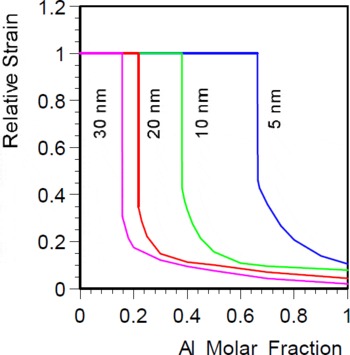
In Ref. Reference Bykhovski, Gaska and Shur24, the sheet electron density was calculated assuming that the spontaneous polarization at zero strain is negligible. In Ref. Reference Shur, Bykhovski, Gaska, Khan, Francombe and Wood12, the calculation of n s was repeated using the spontaneous polarization values estimated in Ref. Reference Bernardini, Fiorentini and Vanderbilt20. Figures 6 a, b show the calculated strain and the sheet electron density, n s , generated by the piezoelectric doping in AlxGa1−xN/GaN HFETs as a function of the Al molar fraction.Reference Shur, Bykhovski, Gaska, Khan, Francombe and Wood 12 The calculation of n s (solid lines in Fig. 6b) accounted for the strain relaxation in HFETs with the AlGaN barrier thicknesses from 5 nm to 30 nm (Fig. 6a). Dashed lines in Fig. 6b correspond to fully strained structures. Also, n s was calculated for the AlxGa1-xN thickness, L, equal to the critical thickness, L c , for a given Al concentration (see thick solid line in Fig. 6b).

Fig. 6a. Calculated strain as a function of Al molar fraction for various AlxGa1-xN layer thicknesses equal to 5 nm, 10 nm, 20 nm and 30 nm.

Fig. 6b. The n s induced by polarization in AlxGa1-xN-GaN heterostructures for various barrier thicknesses. Arrows show the onset of strain relaxation. Thick solid line shows n s corresponding to critical thicknesses of AlGaN. 12
The results show that thinner AlxGa1-xN layers with larger Al content should yield a higher piezoelectric doping. For example, the maximum piezoelectric doping for an unrelaxed heterostructure with L = L c = 5 nm is n s ∼ 3× 1013 cm−2, which corresponds to x ∼ 0.6. This is three times larger than the sheet electron density for L = L c = 20 nm and x = 0.2.
We also measured the C-V characteristics of Al0.25Ga0.75N/GaN heterostructures with thicknesses of Al0.25Ga0.75N ranging from 10 nm to 100 nm using standard mercury probe technique. We calculated the C-V characteristics accounting for strain by using Eq. (6) with strain u xx adjusted to fit the experimental data (see Fig. 7). A similar approach was used in order to determine the elastic strain relaxation in GaN-AlN-GaN SIS structures. Reference Bykhovski, Gelmont, Shur and Khan 22 , Reference Bykhovski, Gelmont, Shur and Khan 23 Figure 6 clearly shows that an increase in Al mole fraction in the AlGaN barrier leads to a higher built-in strain and piezoelectric doping of strained AlGaN/GaN heterostructures. A high value of n s that can be achieved using the piezoelectric doping points to a high potential of piezoelectric doping as a possible substitute (or an important addition) to conventional impurity doping. The critical thickness of the AlxGa1-xN barrier decreases with an increase in the Al molar fraction. This, in turn, reduces the depletion charge in the fully strained AlGaN barrier layer. Also, for x > 0.4, AlxGa1-xN usually becomes insulating. Therefore, in high-quality fully strained AlGaN/GaN heterostructures with high aluminum content, the dominant contributions to the electron gas sheet density should come from the piezoelectric doping as well as from the GaN channel doping. Reference Shur and Khan 11 , Reference Shur and Khan 34

Fig. 7. Measured and calculated (solid lines) capacitance-voltage characteristics of Al0.25Ga0.75 N/GaN structures for different Al0.25Ga.0.25 N layer thicknesses. Curve 1 is for 10 nm, curve 2 is for 20 nm, curve 3 is for 40 nm, curve 4 is for 60 nm, and 5 is for 100 nm. The structures 1, 2 are fully strained, 3, 4 and 5 correspond to elastic strain relaxation of 40%, 70% and 100%. Donor concentrations are Nd = 5×1017 cm−3 and 1017 cm−3 in Al0.25Ga0.75N and GaN layers, respectively. (After Reference Bykhovski, Gaska and Shur 24 )
The results obtained by other groups confirm the importance of the piezoelectric doping. Maeda et al. Reference Maeda, Nishida, Kobayashi and Tomizawa 35 calculated the maximum two-dimensional electron gas density in AlxGa1-xN/GaN HFETs by self-consistently solving Schrodinger’s and Poisson’s equations and accounting for the piezoelectric effect. The maximum 2D-electron gas density was defined as a critical density at which electrons start to spill over into the AlxGa1-xN barrier. The calculated 2D-electron density was in the 2×1012 cm−2−1.2×1013 cm−2 range, depending on the Al molar fraction in the barrier layer, which varied in the range 0.15<x<0.3, and on the degree of strain relaxation. These calculations assumed that strain relaxation could occur even in HFET with the Al content as low as x = 0.15 and AlxGa1-xN thickness 15 nm.
Spontaneous Polarization
First-principle calculationsReference Bernardini, Fiorentini and Vanderbilt 20 predict that spontaneous polarization in wurtzite III-Nitrides should be quite large. A large spontaneous polarization can cause a large internal electric field and strongly affect the band structure. However, the role of the spontaneous polarization depends on the mechanism of the screening of the internal electric field in the bulk of the pyroelectric material and/or at the heterointerfaces. In equilibrium, i.e. without strain or a heat flow, pyroelectric charges are usually compensated by either ambient charges or internal charges forming an equal and opposite dipole moment. An average (macroscopic) internal electric field in heterostructures and superlattices is usually compensated.Reference Ivchenko and Pikus 36
In principle, an internal electric field caused by the pyroelectric charge might generate free electrons and holes even in an insulator due to band bending. However, inversion domains with polarization pointing in opposite directions might cancel the macroscopic electric field and reduce an overall energy of the structure (for the experimental evidence of inversion domains in GaN, see Reference Romano, Northrup and O’Keefe 37 ). The analysis of the piezoresistive measurements in GaN-AlN-GaN SIS structures also provided evidence for the existence of the inversion domains in III-Nitrides.Reference Gaska, Yang, Bykhovski, Shur, Kaminski and Soloviev 38
Another important screening mechanism is linked to the existence of a large number of surface and interface states in pyroelectrics. If the surface state density equals to P s /q, the charges trapped in surface and/or interface states can cancel the spontaneous polarization, making an internal electric field vanish inside the film. Indeed, internal electric fields in pyroelectric materials are usually much smaller than predicted by the theory, which does not ccount for surface and interface states. Reference Fridkin 39 , Reference Selyuk 40 Attempts to find even a trace of an internal electric field at the surfaces of a number of ferroelectrics did not yield any definite results.Reference Fridkin 39 The maximum value of a spontaneous polarization charge, ∼1014 cm−2, observed for all known ferroelectrics is equal to a maximum value of a density of slow and fast surface states in these materials.Reference Fridkin 39 The effect of the current-voltage characteristic collapse in some AlGaN-GaN heterostructures indicates the existence of a large number of interface states Reference Khan, Shur, Chen and Kuznia 41 Reference Khan, Shur, Chen, Kuznia and Sun 42 , at least in some samples
The measurements of the current-voltage characteristics of GaN-AlN-GaN SIS structures seem to show that the effect of the spontaneous polarization is smaller than that of the polarization induced by the piezoelectric effect. Reference Bykhovski, Gelmont, Shur and Khan 23 Hence, further theoretical and experimental studies are needed in order to elucidate a possible role played by spontaneous polarization in GaN-based structures.
Conclusions
GaN-based materials exhibit strong piezoelectric and pyroelectric effects. Both primary and secondary pyroelectric effects have been observed in GaN based structures. These effects are a combination of a fast response to an initial thermal flow and a slower response to heat dissipation or accumulation. The extracted pyroelectric voltage coefficients of GaN are comparable to those of the pyroelectric ceramics such as PZT or BaTiO3. Also, GaN-based pyroelectric sensors should be capable of operating at very high temperatures, and, hence, have an advantage compared to more traditional pyroelectric sensors.
Piezoelectric effects in GaN and related materials can be used both for piezoelectric sensors and for “energy gap engineering” and “barrier engineering” in GaN-based transistors and other electronic and optoelectronic devices.
The demonstrated piezoresistive effect in GaN/AlN multilayer structures is 2 to 4 times larger than in SiC. Reference Gaska, Yang, Bykhovski, Shur, Kaminski and Soloviev 38 Hence, GaN-based structures can be used in pressure transducers and other electromechanical sensing elements.
However, all these applications are still emerging, and further theoretical and experimental studies are needed. A definite set of piezoelectric constants for GaN-based materials has to be established. The transient response of piezoelectric charge should be investigated in more detail. The role of spontaneous polarization, the role of surface and interface states, and of the inversion domains must be ascertained. The piezoelectric doping should be optimized. Further detailed theoretical and experimental studies of strain and dislocations in GaN-based structures are needed in order to better understand the observed stress-related effects and use these effects for the design of novel piezoelectronic and pyroelectronic devices.
New piezoelectronic and pyroelectronic device concepts will certainly emerge to take a full advantage of the unique properties of GaN-based materials. All in all, the recent research of wide band gap semiconductors with wurtzite crystal structure has opened a new dimension in semiconductor physics and device research. And the work has just begun.
Acknowledgments
The Office of Naval Research has supported this work (Project Monitors Dr. Colin Wood and Dr. John Zolper).