Introduction
There have been numerous recent attempts to prepare AlGaN-based heterostructures on Si (111) substrates [Reference Stevens, Kinniburgh and Beresford1-Reference Marchand, Zhang, Zhao, Golan, Rosner, Girolami, Paul, Ibbetson, Keller, DenBaars, Speck and Mishra4]. The achievements of plasma assisted MBE (PAMBE) of AlN and GaN on Si(111) have been summarized in [Reference Yasutake, Takeuchi, Kakiuchi and Yoshii5, Reference Calleja, Sánchez-García, Sánchez, Calle, Naranjo, Muñoz, Molina, Sánchez, Pacheco and García6]. GSMBE, with direct decomposition of NH3 on the substrate surface,[Reference Godlewski, Bergman, Monemar, Rossner and Barski7] can also be used to grow high quality AlN [Reference Nikishin, Antipov, Francoeur, Faleev, Seryogin, Elyukhin, Temkin, Prokofyeva, Holtz, Konkar and Zollner8] and GaN [Reference Godlewski, Bergman, Monemar, Rossner and Barski7, Reference Hellman, Buchanan and Chen9-Reference Lee, Powell, Kim and Greene11]. In the present paper we describe growth of AlN and GaN by GSMBE with NH3 on Si(111) substrates.
We use in situ reflection high-energy electron diffraction (RHEED), low energy electron diffraction (LEED) and ex situ triple-crystal x-ray diffraction (XRD), transmission electron microscopy (TEM), RS, and PL to study structure and optical properties. XRD results from AlN and GaN layers, grown by HVPE on the GSMBE AlN and GaN layers are also reported.
Experimental Details and Discussion
All growth experiments were carried out on 2 and 3-in oriented Si (111) substrates prepared by wet chemical etching [Reference Antipov, Nikishin and Sinyavskii12]. The procedure used results in a hydrogen terminated Si surface. Substrates prepared by this process showed the (7×7) surface structure, observed by RHEED, after heating to 920 K for few minutes. The well known Si(111) surface reconstruction transition, from (7×7) to (1×1), which occurs at Tt=1100 K [Reference Lander13, Reference Osakabe, Tanishiro, Yagi and Honjo14], provided a convenient temperature calibration point [Reference Hellman, Buchanan and Chen9].
It is well known that once the growth chamber is used for the growth of nitrides, the residual nitrogen at the temperature range of 1100−1200 K induces formation of Si-N bonds on the substrate surface [Reference Marchand, Zhang, Zhao, Golan, Rosner, Girolami, Paul, Ibbetson, Keller, DenBaars, Speck and Mishra4-Reference Calleja, Sánchez-García, Sánchez, Calle, Naranjo, Muñoz, Molina, Sánchez, Pacheco and García6, Reference Antipov, Nikishin, Zubrilov, Tsvetkov and Ulin15]. The exposition of Si under the active nitrogen flux during PAMBE results in formation of thick SiN layers (down to ∼1.5 nm) [Reference Nakada, Aksenov and Okumura16]. The formation of amorphous SiN islands leads to disordered growth of AlN and GaN on Si [Reference Calleja, Sánchez-García, Sánchez, Calle, Naranjo, Muñoz, Molina, Sánchez, Pacheco and García6, Reference Ohtani, Stevens and Beresford17]. Different initial treatments have been tried during MBE to eliminate SiN formation. These are mostly based on the use so-called Al/Si γ-phase as starting surface for AlN growth [Reference Yasutake, Takeuchi, Kakiuchi and Yoshii5, Reference Calleja, Sánchez-García, Sánchez, Calle, Naranjo, Muñoz, Molina, Sánchez, Pacheco and García6, Reference Hellman, Buchanan and Chen9, Reference Bourret, Barski, Rouvière, Renaud and Barbier18, Reference Schenk, Kipshidze, Lebedev, Shokhovets, Goldhahn, Ktäußlich, Fissel and Richter19]. However, above 1100K Al/Si γ-phase does not completely protect the Si surface. Approximately 34% of the total substrate area remains bare Si [Reference Yasutake, Takeuchi, Kakiuchi and Yoshii5] when the AlN growth is initiated. This situation deteriorates at higher temperatures (> 1190 K) where the best AlN crystal perfection can be achieved [Reference Calleja, Sánchez-García, Sánchez, Calle, Naranjo, Muñoz, Molina, Sánchez, Pacheco and García6, Reference Calleja, Sánchez-García, Monroy, Sánchez, Muñoz, Sanz-Hervás, Villar and Aguilar20].
The background pressure of NH3 in our Riber-32 was ∼ 5×10⁻⁸ torr. Since the efficiency of NH3 decomposition at the 1100 K is less than a few percent [Reference Powell, Lee and Greene21], we estimate the background beam-equivalent pressure (BEP) of the potentially active NH3 ∼ 10−10 torr. We have shown [Reference Nikishin, Antipov, Francoeur, Faleev, Seryogin, Elyukhin, Temkin, Prokofyeva, Holtz, Konkar and Zollner8, Reference Nikishin, Faleev, Temkin and Chu22] that under these conditions the formation of Al/Si γ-phase is inhibited by SiNx or SiNH [Reference Rzhanov23] islands. These islands form due to the presence of active nitrogen from the background ammonia in the growth chamber.
In order to control the process of silicon nitridation by background NH3, high growth temperature (1130−1190 K), combined with carefully controlled alternating pulses of Al and NH3 [Reference Nikishin and Temkin24], have been employed [Reference Nikishin, Antipov, Francoeur, Faleev, Seryogin, Elyukhin, Temkin, Prokofyeva, Holtz, Konkar and Zollner8, Reference Nikishin, Faleev, Antipov, Francoeur, Peralta, Seryogin, Temkin, Prokofyeva, Holtz and Chu10, Reference Nikishin, Faleev, Temkin and Chu22]. The onset of epitaxy thus suppresses formation of SiNx and results in very rapid transition to 2D growth mode of AlN [Reference Nikishin, Antipov, Francoeur, Faleev, Seryogin, Elyukhin, Temkin, Prokofyeva, Holtz, Konkar and Zollner8]. But, the in situ RHEED control of Si nitridation by background NH3 is a very complicated task. Figure 1 (a) shows a typical RHEED pattern resulting from partial nitridation of Si (111) surface by background NH3, which happens at temperatures above 920 K. To confirm that this pattern is related to the N-Si bond formation, the surface was exposed to higher NH3 flux (up to BEP ∼10−6 torr) and for different durations. The symmetry of the pattern does not change with exposure time up to 2 min. (920−1200 K, NH3 BEP ∼10−6 torr). Beyond 2 min., discrete RHEED reflections disappear suggesting full surface coverage SiNx. The pattern in figure 1 (a) also did not change with temperature (down to 300 K) or with different electron energy of ∼ 5−9 keV.

Figure 1. RHEED patterns along the Si [110} azimuth: (a) partially nitrided Si (111). Position of the (01), (00), and (−01) reflection from the (1×1) structure are indicated from top to the bottom; the extra reflection arise from partial nitridation with NH3; (b) (1×1) surface structure of the first monolayer of AlN.
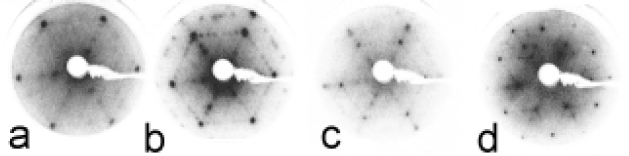
In contrast, LEED measurements provide important details about the Si surface due to the shallower region it probes. Figure 2 shows room temperature LEED patterns of Si (111) surface after NH3 exposure at AlN growth temperature. The pattern, corresponding to an ordered surface, only arises after exposure under background NH3 for the 1–15 min. or under NH3 flux with BEP∼10−6torr for 1−2 s. We observe extra reflections in the LEED images at different electron energies (20−110 eV), i.e., over the range most sensitive to surface structure. The extra reflections vanish under high or prolonged NH3 exposure. The presence of the extra reflections in the LEED pattern signal a well ordered surface of the Si substrate, which is found to be best suited for high quality AlN growth.

Figure 2. LEED patterns of an ordered partially nitrided Si (111) surface at different energy of electron beam: (a) Ee=23 eV; (b) Ee=35 eV; (c) Ee=53 eV; (d) Ee=108 eV. All the RHEED and LEED patterns are displayed as negative images for clearness.
We grew AlN at 1160 ± 30 K. The formation of the (1×1) surface structure could be seen both by RHEED (figure 1 (b)) and LEED after deposition of 2−3 nm of AlN. The growth was started by turning on both Al and NH3 after deposition at least one monolayer of AlN. Growth rates of 90−400 nm/h were obtained. A completed 2D growth mode could be seen, by RHEED, after about 5−7 nm. The rapid transition to 2D growth is of interest for several reasons. First, it results in complete relaxation of AlN [Reference Bourret, Barski, Rouvière, Renaud and Barbier25] by the formation of a coincidence lattice at AlN/Si interface [Reference Schenk, Kipshidze, Lebedev, Shokhovets, Goldhahn, Ktäußlich, Fissel and Richter19]. Second, the rapid transition results in a decrease in both the defect density [Reference Nikishin, Antipov, Francoeur, Faleev, Seryogin, Elyukhin, Temkin, Prokofyeva, Holtz, Konkar and Zollner8, Reference Nikishin, Faleev, Temkin and Chu22] and in the strain energy of AlN layer [Reference Kipshidze, Schenk, Fissel, Kaiser, Schulze, Richter, Weihnacht, Kunze and Ktäusslich26]. From RHEED images we have found the {bSi(111)=(aSi/√2)}/aAlN(0001) ratio of ∼1.233 [Reference Nikishin, Antipov, Francoeur, Faleev, Seryogin, Elyukhin, Temkin, Prokofyeva, Holtz, Konkar and Zollner8]. This compares to 1.235 obtained from standard values of lattice constants of Si (aSi=0.542 nm) and AlN (aAlN=0.311 nm). Thus the condition 4:5 along [110] azimuth of Si is evident. A similar effect of matching has been observed for c-GaN/GaAs(001) interface [Reference Trampert, Brandt, Yang and Ploog27].
The growth of GaN was started after AlN buffer layer completed the transition to the 2D growth mode. GaN layers were grown at a temperature of 1000±30 K and growth rates of 0.4−5 μm/h. Formation of a (2×2) surface structure could be seen by RHEED after deposition of 20−100 nm of GaN. The fastest 3D-2D transition of growth mode was reached at the highest growth rate, possibly due to the high value of lateral growth rate reported for GaN [Reference Moustakas28]. We also prepared structures incorporating several (1−4) short period AlN/GaN and AlGaN/GaN superlattices (SLs). The effectiveness of such SLs, in controlling defect propagation from the AlN/Si and AlN/GaN interfaces, is demonstrated in the TEM cross section of figure 3. We stress that the third GaN layer and SL (figure 3) were grown in a 2D growth mode with (2×2) surface structure. Recently, similar SLs has been used to improve crystal quality of GaN grown on Si(001) by metal-organic chemical vapor deposition (MOCVD) [Reference Zhang, Chua, Li, Chong and Feng29].

Figure 3. TEM cross-section of GaN/(buffer layer)/Si structure.
From XRD measurements the full width at half maximum (FWHM) of the (0002) AlN peak in triple-crystal ω−2θ scan was less than 100 arc sec. This is the best value reported for ∼200 nm thick AIN grown on Si(111). In GaN samples 1.5−2 μm thick the FWHM of the (0002) peak was as narrow as 14 arc sec. The GaN layers were free of cracks.
The layers of GaN grown on silicon are known to crack during the cool-down cycle (see references in [Reference Nikishin, Antipov, Francoeur, Faleev, Seryogin, Elyukhin, Temkin, Prokofyeva, Holtz, Konkar and Zollner8]). Cracking is believed to occur due to the thermal expansion coefficient mismatch between GaN and Si. Based on the result present both in this article and [Reference Nikishin, Faleev, Antipov, Francoeur, Peralta, Seryogin, Temkin, Prokofyeva, Holtz and Chu10, Reference Schenk, Kipshidze, Lebedev, Shokhovets, Goldhahn, Ktäußlich, Fissel and Richter19, Reference Nikishin, Faleev, Temkin and Chu22, Reference Nikishin and Temkin24-Reference Kipshidze, Schenk, Fissel, Kaiser, Schulze, Richter, Weihnacht, Kunze and Ktäusslich26], we can assume that cracking of GaN can be completely eliminated by assuring uniform growth of AlN at the Si-N-Al interface. From Raman measurements [Reference Nikishin, Faleev, Antipov, Francoeur, Peralta, Seryogin, Temkin, Prokofyeva, Holtz and Chu10] we found the value of a residual tensile stress of < 0.2 GPa in our GaN with the thickness of 0.4−2.3 μm. This low stress is important because it is well below the ultimate strength of breaking of 0.4 GPa, under tensile stress, for GaN [Reference Pankove and Moustakas31].
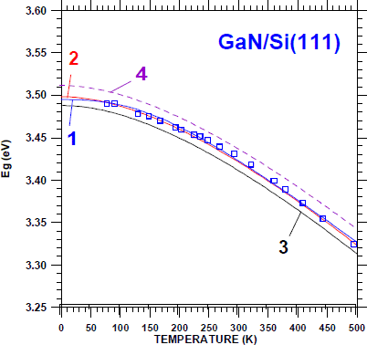
PL spectra at temperatures ranging from 77K to 495K were excited by a 2 kW pulse (10ns, 100Hz) nitrogen laser. Above 100 K, the PL spectra are dominated by the free exciton (FE) recombination [Reference Monemar, Bergman, Buyanova, Li, Amano and Akasaki32, Reference Smith, Chen, Lin, Jiang, Khan, Sun, Chen and Yang33]. The red shift of the FE peak, due to the bandgap shrinkage, as well as usual quenching were observed with increasing temperature. The room temperature PL spectra of GaN show a FE peak position at 3.408 eV with the FWHM of less than 40 meV. The temperature dependence of the bandgap energy calculated from PL data for our GaN/Si crystals is presented in figure 4. Experimental data were fitted with both Passler’s model [Reference Passler34] and Varshni’s empirical approximation [Reference Varshni35]. The PL results will be reported in detail in a later paper [Reference Zubrilov, Nikishin and Temkin36]. Also presented in figure 4 is the temperature dependence of the bandgap energy for a GaN layer grown by MOCVD on 6H-SiC substrate [Reference Zubrilov, Nikolaev, Tsvetkov, Dmitriev, Irvine, Edmond and Carter37] and for a stress-free bulk GaN crystal grown HVPE [Reference Zubrilov, Melnik, Nikolaev, Jakobson, Nelson and Dmitriev38]. Comparison of the Eg(T) dependence for GaN grown on Si(111) and on SiC substrates, with that of bulk GaN indicates residual tensile mechanical stresses in epilayers on both substrates. For GaN/SiC this has a value of about 0.5−1.0 GPa, which is primarily due to differences in values of the thermal expansion coefficients of GaN and SiC. This is at twice as large as what we see in our GaN/Si samples. That is why the Eg(T) dependence is closer to that for strain free bulk GaN as shown in figure 4. Our estimation of the tensile stresses in our GaN/Si samples, based on the PL measurements, ranges from 0.08 to 0.3 GPa. These values are in a good agreement with the results of our Raman measurements.

Figure 4. The temperature dependence of the bandgap. Squares – this work; 1 - Passler’s model [Reference Passler34] fit; 2 – Varshni’s model [Reference Varshni35] fit; 3 – GaN layer grown by MOCVD on SiC (recalculated data from [Reference Zubrilov, Nikolaev, Tsvetkov, Dmitriev, Irvine, Edmond and Carter37]; 4 – Strain free bulk GaN grown by HVPE [Reference Zubrilov, Melnik, Nikolaev, Jakobson, Nelson and Dmitriev38].
The AlN and GaN layers grown by MBE on Si were used as substrate materials for growth of thick AlN and GaN layers by HVPE. The FWHM of the AlN (0002) ω−2θ-scan peak in the structure AlN(50 µm thick, HVPE)/GaN-AlN(MBE)/Si was 93 arcsec. For a 50 μm thick AlN layer grown by HVPE directly on Si, a FWHM value of 61 arcsec was obtained. FWHM of (0002) GaN peak in the structure GaN(1.5 μm thick, HVPE)/GaN-AlN(MBE)/Si at ω−2θ-scan was 48 arcsec. The c-axis lattice constant of HVPE GaN was higher than that of MBE grown GaN. We are currently performing experiments to understand this phenomenon.
Conclusions
This study shows how to grow high quality of GaN and AlN by GSMBE with NH3. We can conclude that cracking of GaN grown on Si (111) can be completely eliminated by assuring uniform growth of AlN at the Si-N-Al interface.
Acknowledgements
Work at TTU is supported by DARPA (monitored by Dr. Robert F. Leheny), AFOSR (monitored by Major Dan Johnstone) and the J. F Maddox Foundation.