Introduction
GaN and AlGaN are currently of great interest for application to ultraviolet (UV) laser diodes (LDs) and light-emitting diodes (LEDs) [Reference Nakamura and Fasol1,Reference Han, Crawford, Shul, Figiel, Banas, Zhang, Song, Zhou and Nurmikko2], because the wide band gap direct transition can be adjusted between 6.2eV (AlN) and 3.4eV (GaN). Recently, UV LDs or LEDs are expected to realize the large capacity optical memories, new chemical processes, medical applications and disposal facilities to industrial wastewater [Reference Ogita, Hatta, Nishimoto and Kagiya3].
Some research groups reported on the approaches to the realization of UV optical devices using GaN or AlGaN materials [Reference Kozodoy, Hansen, DenBaars and Mishra4,Reference Mukai, Narimatsu and Nakamura5]. We have already achieved 333 nm current injection emission from Al0.03Ga0.97N/Al0.25Ga0.75N quantum wells (QWs) and 234 nm efficient photoluminescence from AlN/AlGaN QWs. However there are some large problems preventing them from achieving UV optical devices. The most serious problems are difficulty to obtain efficient UV emission from AlGaN QWs, in contrast to InGaN QWs, and current injection through high Al content (more than 30%) AlGaN alloy. The emission enhancement in GaN/AlGaN QWs using Si- or In- [Reference Shen and Aoyagi6] doping have been reported, and some mechanisms of the emission enhancement were discussed in previous papers [Reference Han and Crawford7-Reference Schubert, Goepfert, Grieshaber and Redwing9]. However, the dominant mechanism of them was not yet clarified.
In this paper, we systematically investigate the PL intensity enhancement induced by Si-doping into GaN/AlGaN single (S) and multi quantum well (MQW) structures and reveal that the dominant effect is due to screening of piezoelectric field in the QWs. At first, the PL intensity enhancement due to Si-doping is compared between well doping MQWs and barrier doping ones. Then, the dependencies of Si-doping concentration and well thickness on the PL enhancement for the SQWs are investigated. Finally, the maximum blue shift by changing the PL excitation power is compared between Si-doped and undoped SQWs.
Sample Preparation
The samples were grown at 76 Torr on the Si faces of on-axis 6H-SiC(0001) substrates by a conventional horizontal-type metal organic vapor phase epitaxy (MOVPE) system. The substrates were loaded onto a SiC-coated graphite susceptor inductively heated by RF. As precursors, ammonia (NH3), tetraethylsilane (TESi), trimethylaluminum (TMAl), and trimethylgallium (TMGa) were used with H2 or N2 as carrier gas. Typical gas flows were 2 standard (at 760 Torr) liters per minute (SLM), 2 SLM, and 2 SLM for NH3, H2, and N2, respectively. The molar fluxes of TMGa and TMAl for AlGaN growth were 38 and 4.2 μmol/min, respectively. The substrate temperature during growth was measured with a thermocouple located at the substrate susceptor.
In order to achieve a surface suitable for growth of GaN QWs, first an approximately 500 nm-thick Al0.15Ga0.85N buffer layers following extremely thin (∼ 5 nm) AlN layers were deposited on a 6H-SiC substrate at 1100°C. Then 5 layers of MQW or SQW of GaN/AlGaN was grown at 1080°C. The well widths were ranging from 2 to 5 nm. The barrier width was 6 nm. Si was doped to the well layer(s) or barrier layers, and the doping concentration was ranging up to 9×1018 cm−3. Finally, a 25-nm-thick Al0.15Ga0.85N cap layer was grown at the same temperature as used for the QWs. The thickness of each layer was estimated based on the growth rate of equivalent bulk samples. The full width at half maximum of the X-ray rocking curve of bulk GaN and AlGaN sample were 95 sec and 122 sec, respectively. All of the PL measurement was performed at 77 K under He-Cd laser excitation except for the last measurement (Fig. 5).
Measurement Results and Discussion
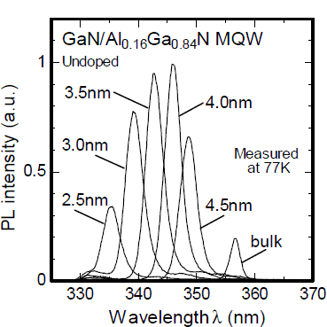
At first, the well width dependence of PL properties of undoped MQWs was investigated in order to find the optimized well width for PL intensity. Figure 1 shows the PL spectra of undoped GaN/Al0.16Ga0.84N 5MQWs with various well widths. The intense single peak emission from QW regions were observed. The peak wavelength was shifted from 335 nm to 339 nm when the well width was varied from 2.5 to 4.5 nm. The measured PL peak energy agrees well with the theoretical value calculated taking into account piezoelectric field in the well. The emission around at 332 nm is from barrier layers. The phonon-replica peak was observed at lower energy side of the QW’s peak indicating the high crystal quality of the QWs. The PL intensity heavily depends on the well width.

Figure 1. PL spectra of undoped GaN/Al0.16Ga0.84N 5MQWs with various well width measured at 77K. The PL peak energy and intensity strongly depend on the well width.
The reason for the immediate PL intensity reduction for thick MQWs is explained by the separation of electron and hole wave functions induced by the large piezoelectric field in the QWs [Reference Chichibu, Cohen, Mack, Abare, Kozodoy, Minsky, Fleischer, Keller, Bowers, Mishra, Coldren, Clarke and DenBaars8]. For thin MQWs, the broadening of electron wave function and an increase of nonradiative transition at heterointerfaces induces the reduction of PL intensity. The strongest PL intensity was obtained for 4nm-thick MQW. For SQW samples, we obtained almost the same well width dependence.
Then well doping and barrier doping samples were compared with respect to the PL intensity enhancement ratio in GaN/Al0.16Ga0.84N five layer MQW structures. Figure 2 shows the PL enhancement ratio compared with undoped one as a function of Si-doping concentration for well doping and barrier doping samples. The well width was 4 nm, which was the optimum value for undoped case. Si-doping concentration was varied ranging from 0 to 9×1018 cm−3. The enhancement ratio strongly depends on the Si-doping concentration. The larger value of enhancement ratio was obtained for well doping cases. The Si-doping concentration, which gives the maximum enhancement ratio, was smaller for well doping. The typical value of the enhancement ratio was seven times for well doping of 3×1018 cm−3, and three times for barrier doping of 5×1018 cm−3. For both series of samples, the enhancement ratio increases with an increase of doping concentration at the beginning, then reduces for higher doping concentration. The mechanism of PL intensity enhancement is based on the screening of the piezoelectric field in the wells that is to be mentioned in detail later. The enhancement ratio reduction at high doping concentration is induced by the deterioration of the crystal quality.

Figure 2. PL intensity enhancement ratio for Si-doped GaN/Al0.16Ga0.84N 5MQWs as a function of Si-doping concentration. Si is doped in the wells or barriers. The well and barrier width were 4nm and 6nm, respectivery.
We discuss the mechanism of PL intensity enhancement due to Si-doping. Some previous works reported about the influence of Si-doping in bulk GaN [Reference Schubert, Goepfert, Grieshaber and Redwing9] or barrier layers of InGaN MQWs [Reference Chichibu, Cohen, Mack, Abare, Kozodoy, Minsky, Fleischer, Keller, Bowers, Mishra, Coldren, Clarke and DenBaars8], but there is no report about the comparison of well doping and barrier doping. In this work, the well doping is shown to be more efficient for GaN system, in contrast to the modulation doping (barrier doping) method which was widely applied for GaAs or InP systems. This is because the influence of the deterioration in GaN system is smaller than that in the other materials. This result seems to be notable as evidence for the peculiarity of this material.
There are two effects of Si-doping considered to induce the PL enhancement. One is screening of piezoelectric field in the wells, and the other is improvement of crystal quality. The screening effect is determined by an increase of carrier concentration and also a lattice stress relaxation of the well [Reference Ruvimov, Weber, Suski, Ager, Washbum, Krueger, Kisielowski, Weber, Amano and Akasaki11]. The effective carrier concentration in the well is larger for well doping case. For barrier doping case, the carrier injected from the barrier layers causes the same effect [Reference Chichibu, Cohen, Mack, Abare, Kozodoy, Minsky, Fleischer, Keller, Bowers, Mishra, Coldren, Clarke and DenBaars8]. In the GaN/AlGaN QWs, the well is expected to be compressively strained. In our experiment the value of compressive strain in the well is estimated to be approximately 0.64% simply from the lattice constant of GaN and Al0.14Ga0.86N. By introducing Si-doping in GaN, the compressive strain is expected to be slightly relaxed [Reference Ruvimov, Weber, Suski, Ager, Washbum, Krueger, Kisielowski, Weber, Amano and Akasaki11], because Si in GaN shortens the lattice constant along c-axis. However, the value of the stress relaxation by Si-doping is reported to be small in case doping level is 1018-1019 cm−2 (for example 0.027% for Si-doped GaN on sapphire [Reference Ruvimov, Weber, Suski, Ager, Washbum, Krueger, Kisielowski, Weber, Amano and Akasaki11] or negligible value for Si-doped GaN/InGaN QWs [Reference Cho, Song, Keller, Minsky, Hu, Mishra and DenBaars12]). Consequently, the carrier increasing is considered to be dominant for the screening of piezoelectric field.
On the other hand, improvement of crystal quality due to Si-doping causes the reduction of luminescence killers [Reference Schubert, Goepfert, Grieshaber and Redwing9]. The reduction of defects, which is reported by S. Ruvimov et al., is expected to occur for every Si-doped sample in this experiment [Reference Ruvimov, Weber, Suski, Ager, Washbum, Krueger, Kisielowski, Weber, Amano and Akasaki11]. In our experiments, no drastic difference of the line width of PL spectra between well doping and barrier doping was observed. Hence, the screening of the piezoelectric field in the wells is considered to be the dominant mechanism of the PL intensity enhancement.
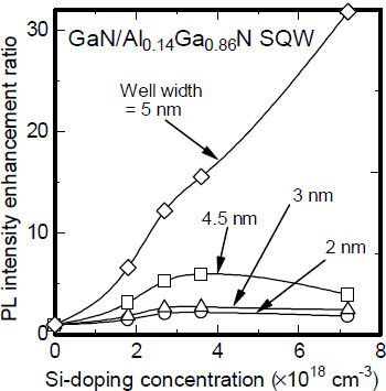
Figure 3 shows the PL intensity enhancement ratio of Si-doped GaN/Al0.10Ga0.90N SQWs for various well widths as a function of Si-doping concentration. SQW structures were used in order to minimize the influence of well width fluctuation and the piezoelectric field of barrier layers. Si was doped only in the well. The well width and Si-doping concentration was varied from 2 to 5 nm, and from 0 to 8×1018 cm−3, respectively. The maximum value of the enhancement ratio increased with the increase of well width. The typical value was 30 times for 5 nm-thick SQW of 8×1018 cm−3 Si-doped. For every well width, the enhancement ratio saturates at high doping concentration. The Si-doping concentration at the saturated region is higher for thick well. This is because for thick QW the piezoelectric field is strong and then high doping was needed to screen the field. These results fairly explain that screening of the piezoelectric field in the well induces the PL intensity enhancement.

Figure 3. PL intensity enhancement ratio for Si-doped GaN/Al0.14Ga0.86N SQWs with various well width as a function of Si-doping concentration.
Figure 4 shows the PL peak shift for Si-doped SQWs from that obtained for the undoped sample as a function of Si-doping concentration. The PL peak energy shows a large blue shift at low Si-doping concentration, and then a gradual red shift. The amount of the blue shift was larger for thick SQWs. The blue shift is considered due to the screening of the piezoelectric field in the well. The amount of blue shift becomes large for a thick QW, because the piezoelectric field becomes stronger. On the other hand, the PL peak red shift at high Si-doping concentration more than 3×1018 cm−3 was considered to be induced by the band gap narrowing due to Si-doping.

Figure 4. PL peak energy shift for Si-doped GaN/Al0.14Ga0.86N SQWs with various well width as a function of Si-doping concentration.
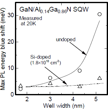
Figure 5 shows the maximum PL peak shift from low to high excitation conditions as a function of well width for Si-doped and undoped SQWs. The well width was varied from 2 nm to 5 nm. The PL measurement was performed at 20K. The excitation lasers used were He-Cd laser (325 nm, approximately 3 W/cm2) and Xe-Cl excimer laser (308 nm, approximately 200 kW/cm2) for low and high excitation conditions, respectively. For Si-doped sample, the maximum blue shift was independent of well width. On the other hand, for undoped sample, the maximum blue shift increased with the increase of the well width. This shows that the piezoelectric field in the Si-doped SQW is screened even under low excitation conditions by electron charge induced by Si-doping.

Figure 5. PL peak energy difference between high and low excitation conditions for undoped and Si-doped GaN/Al0.14Ga0.86N SQWs as a function of well width. Si-doping concentration was 1.8×1018 cm−3.
Conclusions
In conclusion, we systematically study the PL enhancement due to the screening of piezoelectric field induced by Si-doping in GaN/AlGaN QWs fabricated by MOVPE. The PL enhancement ratio of QWs for Si-doped directly into the wells was much larger than that for doped only into the barrier layers. This result shows that the crystal quality of the quantum well is not so damaged by heavy Si-doping, which is different from the cases of GaAs or InP material systems. The PL intensity enhancement ratio was especially large for thick wells. The typical value of the enhancement ratio was 30 times for a 5 nm-thick single QW. The optimum Si-doping concentration was approximately 4×1018 cm−3. From the well width dependence of the PL enhancement ratio and PL peak shift under high excitation conditions, we determined that the dominant effect inducing the PL enhancement is screening of the piezoelectric field in the QWs. These results indicate that Si-doping is very effective for the application of GaN/AlGaN QWs to optical devices.