Introduction
AlGaN/GaN heterostructure field effect transistors (HFETs) have recently been attracting much attention because of their promising uses for high-voltage, high-power, and high-temperature microwave applications [Reference Khan, Chen, Shur, Mcdermott and Higgins1-Reference Ping, Chen, Yang, Khan and Adesida7]. Improving device performances requires an understanding of how we can increase the mobility and the density of the two-dimensional electron gas (2DEG) in this material system. Desirable designs of heterostructures should be investigated for superior transport properties.
In nitride heterostructures with wurtzite crystal structures in (0001) orientation, there exist strong polarization effects, i.e., (i) the piezoelectric polarization effect which depends on the lattice strain [Reference Bykhovski, Gelmont and Shur8], and (ii) the spontaneous polarization effect which is determined by the constituent materials of the heterostructure [Reference Bernardini and Fiorentini11]. These polarization effects largely influence the electrical properties in the heterostructures such as the potential profile and the electron density [Reference Bykhovski, Gelmont and Shur8-Reference Maeda, Nishida, Kobayashi and Tomizawa16].
The 2DEG transport properties in nitride double-heterostructure field effect transistors (DH-FETs) are very interesting, because influence of the polarization effects should be enhanced in DH-FETs, compared with that in conventional single-heterostructure field effect transistors (SH-FETs). In SH-FETs, only the positive polarization charges emerge at one heterointerface; on the other hand, positive and negative polarization charges emerge at two heterointerfaces in DH-FETs, so that the electric field in the channel should be increased in DH-FETs. In this paper, we report on the 2DEG transport properties in DH-FETs and clarify their differences from those in SH-FETs. We propose AlGaN/(In)GaN/AlGaN DH-FETs are effective in enhancing the 2DEG confinement due to the polarization effects, and furthermore effective in increasing the 2DEG mobility.
Experimental Details and Discussion
Comparison of GaN DH and GaN SH
To examine the influence of the enhanced polarization effects in DH-FETs on the transport properties, we have fabricated both conventional AlGaN/GaN SH-FETs and AlGaN/GaN/AlGaN DH-FETs, and have compared their electrical properties.
The sample structures of (a) conventional GaN SH-FETs and (b) GaN DH-FETs are (a) Al0.15Ga0.85N (300 Å) /GaN (1 μm), and (b) Al0.15Ga0.85N (300 Å) /GaN (200 Å) /Al0.15Ga0.85N (1000 Å), respectively. The samples were grown on SiC(0001) substrates using AlN buffer layers by metalorganic vapor-phase epitaxy (MOVPE) at 300 Torr. In all samples, only the surface-side 300 Å Al0.15Ga0.85N barrier layers were uniformly doped with Si.
We have performed Van der Pauw Hall effect measurements on the GaN SH- and GaN DH-FET samples, both of which are doped with the same Si doping concentration of 4×1018 cm−3. Figure 1 shows the temperature dependencies of the 2DEG mobility and the 2DEG density from 20 to 380 K in the two samples. The striking feature shown in Fig. 1 is a drastic increase in the 2DEG mobility in the DH-FET sample. The 2DEG mobility in DH-FET reaches 8900 cm2/Vs at 20 K, whereas that in SH-FET reaches 4600 cm2/Vs. The 2DEG densities at 20 K in DH- and SH-FET samples are 6.5×10¹² and 7.5×1012 cm−2, respectively. This difference in the 2DEG density is not so large as to explain the observed large difference in the 2DEG mobility. Hence, the observed mobility enhancement in DH-FET is a unique phenomenon specific to nitride HFETs.

Figure 1. Temperature dependencies of 2DEG mobility and density in GaN SH- and DH-FETs.
To clarify the dependencies of the 2DEG mobility on the 2DEG density in DH- and SH-FETs, we have performed Hall effect measurements under the gate-voltage application. In this experiment, we have used DH- and SH-FET samples with the Si doping concentration of 5×1018 cm−3. The grown structures were mesa-etched to form a 400×400 μm2 rectangular Van der Pauw geometry device, by using low-damage reactive ion etching (RIE) technique using chlorine-nitrogen mixed plasma [Reference Saitoh, Gotoh, Sogawa and Kanbe17]. The Al/Au ohmic metals were deposited on the corners of the rectangular mesa structure, and the Ni/Au Schottky gate metals was deposited on almost all the area of the device except for the ohmic terminals.
For the above devices, we have performed Hall effect measurement at 4.2 K under the gate voltage (Vg) application. The Vg was stepped from 0 to −2.5 V in −0.25 V increments. In this Vg region, the 2DEG density has shown to be almost linearly controlled by Vg both in DH- and SH-FET samples.
Figure 2 shows the dependence of the 2DEG mobility on the 2DEG density in the DH- and SH-FET samples at 4.2 K. One feature observed in Fig. 2 is that the 2DEG mobility in DH-FET is larger than that in SH-FET. The enhancement in the mobility is very large especially at low 2DEG densities, which is consistent with the result shown in Fig. 1. Another feature observed in Fig. 2 is the shift of the 2DEG mobility peak position. In SH-FET, the maximum 2DEG mobility of 5700 cm2/Vs is obtained at 9.0×1012 cm−2; whereas in DH-FET, the maximum mobility of 8100 cm2/Vs is obtained at a lower 2DEG density of 6.8×1012 cm−2.

Figure 2. Dependencies of 2DEG mobility on 2DEG density in GaN SH- and DH-FETs.
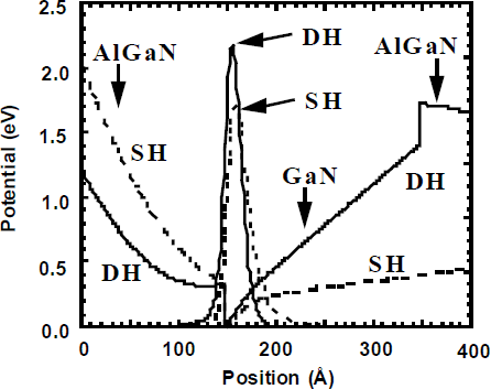
To clarify the mechanism of the mobility enhancement in DH-FET, we have calculated the potential profiles and 2DEG distributions both in the SH- and DH-FETs by self-consistently solving the Schrodinger and Poisson’s equations. Both piezoelectric and spontaneous polarization effects have been taken into account. Figure 3 shows the result calculated for the same 2DEG concentration of 6×1012 cm−2. The 2DEG confinement is enhanced in DH-FET due to the enhanced electric field in the DH channel. Thus, the strongly confined 2DEG and the increased electron concentration in DH-FET lead to enhance the 2DEG mobility, as the result of (i) the enhanced screening effect against the ionized impurity scattering both in the channel and from the barrier layer, and (ii) the enhanced screening effect against the piezoelectric scattering in the channel. Figure 3 also explains why the 2DEG mobility in DH-FET assumes the maximum value at a lower 2DEG density. In DH-FET, the energy barrier height of the surface-side AlGaN layer is shown to be lower as the result of the enhanced electric field in the DH channel. Hence, electrons overflow into the AlGaN layer at the lower critical 2DEG density where the 2DEG mobility assumes the maximum value. This circumstance is ascribed to the feature mentioned above.

Figure 3. Potential profiles and 2DEG distributions in GaN SH- and DH-FETs. The 2DEG dinsity is 6.0×1012 cm−2 in both structures. The Al composition is 0.15.
The observed features in Fig. 2 can be thus explained by the enhanced 2DEG confinement effect in DH-FET. However, we presume that some additional mechanisms should also have contributed to the mobility enhancement, since the observed enhancement is very large. We suppose that the improvement of the interface roughness in DH-FETs should have additionally contributed to the mobility enhancement, because surface morphology is observed to be improved in DH-FETs.
We demonstrate device operation of a GaN. The mesa isolation of the devices was performed by RIE. Ti/Al/Ti/Au and Ni/Au layers were used as the ohmic and Schottky metals, respectively. The gate length and width of the fabricated DH-FET were 0.4 and 20 μm, respectively. Figure 4 shows the I-V characteristics of the device. The maximum transconductance (gm) was estimated to be 180 mS/mm. It should be noted that sufficient pinch-off characteristics have been obtained even in DH-FETs.

Figure 4. I-V characteristics in GaN DH-FET. The gate length and gate width is 0.4 and 20 μm, respectively. The maximum transconductance is 180 mS/mm.
Comparison of InGaN DH and GaN DH
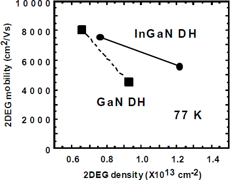
It is of great interest in nitride DH-FETs to use InGaN channels instead of GaN channels, because the capacity for the 2DEG density is expected to be increased in InGaN DH-FETs as the result of the enhanced polarization effect (i.e., increased polarization charges) and the enlarged conduction-band discontinuity at the AlGaN/InGaN heterointerface. We compare the 2DEG mobilities and densities in GaN and InGaN DH-FETs. The In0.06Ga0.94N layer is used as the channel in the InGaN DH-FET.
Figure 5 plots the 2DEG mobility data as a function of the 2DEG density, measured at 77 K in GaN and InGaN DH-FET samples. Here, two different Si doping concentrations (4×10¹⁸ and 6×1018 cm−3) are used in both GaN and InGaN DH-FET samples. At lower 2DEG densities in Fig. 5, the 2DEG mobility in InGaN DH-FET is as high as that in GaN DH-FET: a high mobility of 7600 cm2/Vs is obtained at 77 K for the 2DEG density of 7.6×1012 cm−2. Thus, the 2DEG mobility is enhanced also in the DH-FET with the In0.06Ga0.94N channel.

Figure 5. 2DEG mobilities as a function of 2DEG density in GaN and InGaN DH-FET samples. The In composition is 0.06.
At higher 2DEG densities in Fig. 5, on the other hand, a distinct difference in the 2DEG mobility has been shown. In GaN DH-FET, a mobility of 4500 cm2/Vs is obtained for a relatively high 2DEG density of 9.2×1012 cm−2. In InGaN DH-FET, on the other hand, a mobility as high as 5600 cm2/Vs is obtained for a high 2DEG density of 1.2×1013 cm−2. Thus, the degradation of the 2DEG mobility along with the increase in the 2DEG density is smaller in InGaN DH-FET than in GaN DH-FET. This indicates that InGaN DH-FET has the larger capacity for 2DEG than GaN DH-FET. This is valid also at 300 K. Thus, high 2DEG mobilities and high 2DEG densities can be simultaneously obtained in InGaN DH-FETs.
Conclusion
We have investigated two-dimensional electron gas transport properties in nitride double-heterostructures. A striking effect has been observed that the 2DEG mobility has been drastically enhanced in the AlGaN/GaN/AlGaN double-heterostructure, compared with that in the conventional AlGaN/GaN single-heterostructure. The observed mobility enhancement has been shown to be mainly due to the enhanced polarization-induced electron confinement in the double-heterostructure, and additionally due to the improvement of the interface roughness in the structure. Device operation of an AlGaN/GaN/AlGaN DH-FET has been demonstrated: a maximum transconductance of 180 mS/mm has been obtained for a 0.4 μm-gate-length device. In the double-heterostructure using InGaN channel, the increased capacity for the two-dimensional electron gas has been observed. The AlGaN/(In)GaN/AlGaN double-heterostructures are effective for improving the electron transport properties.
Acknowledgements
The authors would like to thank Dr. Yoshiro Hirayama for his assistance in Hall effect measurements, Dr. Masaaki Tomizawa, Dr. Hirotaka Tanaka and Dr. Hideaki Takayanagi for their assistance in computer calculation, and Dr. Naoshi Uesugi and Dr. Sunao Ishihara for their encouragement throughout this work.