


Introduction
Human beings have long been, and will continue to be, fascinated by Nature and how it works. Curiosity and a thirst for understanding Nature have fueled scientific and technological breakthroughs which have been continuously improving our quality of life. We develop our perception of Nature by sensing of which visualization plays a critical role. Since human eyes have a very limited angular resolution (~1 arcminute or approximately 0.0003 radians), our naked eyes cannot directly visualize either tiny features/creatures, such as individual living bacteria, or gigantic individual stars within constellations that are far away. The early practice of making spectacles and magnifiers with the goal of “seeing” small features more clearly led to the development of two important scientific tools: The telescope for clearly observing things far away and the microscope for examining small features/creatures that our naked eyes could not do. Both the early telescope and microscope relied on the unique properties of glass lenses that possess the power to manipulate light rays. The continuous improvement in telescopes has vastly expanded our knowledge of the Universe, while the development of various types of microscopes has enabled us to directly observe bacteria, viruses, molecules, and even individual atoms. The invention of both the telescope and the microscope has unlocked countless mysteries of Nature and enabled numerous discoveries that have positively impacted our daily life.
In this review, the goal is to account for the major advances in one particular type of microscope that is now broadly used for analyzing matter at the atomic scale: the scanning transmission electron microscope (STEM). Although STEM was used to image single metal atoms as early as 1970 (Crewe et al., Reference Crewe, Wall and Langmore1970), it took a long time for the broader research communities to effectively utilize this powerful characterization method. The practical realization of the correction of lens aberrations to routinely achieve sub-Ångstrom image resolution with picometer precision and high chemical sensitivity greatly enhanced the impact of STEM and associated techniques on many research frontiers. Such an accomplishment has revolutionized how we understand matter at the atomic level and will have a tremendous impact on how we understand Nature. The significance of this accomplishment is evidenced by the recent award of the 2020 Kavli Prize in Nanoscience to Harald Rose, Maximilian Haider, Knut Urban, and Ondrej L. Krivanek “for sub-Ångstrom resolution imaging and chemical analysis using electron beams” (Rose et al., Reference Rose, Haider, Urban and Krivanek2020).
Since many excellent reviews have been published on the topic of aberration-correction (e.g., Rose, Reference Rose2008, Reference Rose2009; Hawkes, Reference Hawkes2009a, Reference Hawkes2009b, Reference Hawkes2015; Septier, Reference Septier2017; Hawkes & Krivanek, Reference Hawkes and Krivanek2019) we will focus, in this review, on the advances of forming high-resolution images by scanning a finely focused electron probe and how to correctly interpret such images. For the fundamental principles and applications of aberration-corrected STEM (ac-STEM), the interested reader is strongly encouraged to read the excellent reviews/books on these topics (Rose, Reference Rose2009; Pennycook & Nellist, Reference Pennycook and Nellist2011; Erni, Reference Erni2014; Tanaka, Reference Tanaka2014; Hawkes & Krivanek, Reference Hawkes and Krivanek2019; Nellist, Reference Nellist, Hawkes and Spence2019).
A Brief History of the Light Microscope and the Birth of the Electron Microscope
The Dutch eyeglass makers Hans Martens/Zacharias Janssen are frequently credited for inventing the compound microscope (Orchard & Nation, Reference Orchard and Nation2014), while Hans Lippershey, another Dutch eyeglass maker, is considered to be the first person to patent a telescope by assembling a concave eyepiece aligned with a convex objective lens (Van Helden, Reference Van Helden1977). The early practical applications of these lens-based telescopes and microscopes were clearly reflected in their respective nicknames as spyglasses and flea glasses. Galileo Galilei, in 1609, constructed his own telescope and discovered that the moon was not a perfect sphere; and with finely polished lenses, he subsequently conducted scientific observations of celestial objects and discovered many distant systems that had not been previously known (Drake, Reference Drake2003). Even though the modern James Webb Space Telescope (expected to be launched in late 2021) may cost more than $10 billion, our understanding of the Universe started by stacking two glass lenses to form a rudimentary telescope.
Although the early development and applications of the scientific microscope are difficult to trace exactly, Robert Hooke's publication of Micrographia in 1665 (Hooke, Reference Hooke1665) clearly demonstrated the power of using compound microscopes to observe tiny features that naked human eyes had not been able to do. Hooke also coined the word “cell” for describing the observed structures of the cork bark under a compound microscope. The discovery of the cell was made possible through the invention of the microscope. Because of the aberrations of poorly polished glass lenses and other related issues, the early compound microscopes could not provide high magnification images without severe image distortion. On the other hand, with a finely polished single glass lens, Antonie van Leeuwenhoek was able to examine a variety of biological specimens in an aqueous environment, even the dynamical movement of tiny creatures, with a magnification as high as ~300× (Lane, Reference Lane2015). Through extensive observations via his refined single-lens microscope, van Leeuwenhoek discovered many secrets of Nature such as bacteria, microscopic protists, sperm cells, blood cells, and microscopic nematodes and rotifers. The invention of the light microscope made the invisible world visible and enabled many discoveries that helped us better understand Nature, created new scientific disciplines, and significantly improved the quality of life of human beings.
To understand how a microscope works and how to reliably produce high-quality light microscopes, Ernst Abbe formulated an imaging theory and established a resolution limit for light microscopes: due to diffraction effect, the wavelength of the light source controls the ultimate attainable image resolution of a light microscope to about half of the wavelength of the light source (Abbe, Reference Abbe1873). Even if the lens aberrations are perfectly corrected, the highest attainable resolution of a light microscope has been limited to about 200 nm. Such a theoretical limit prevented a clear observation of subcellular structures with smaller sizes. The early work on trying to overcome the image resolution barrier by scanning a localized light probe was not very successful (Synge, Reference Synge1928, Reference Synge1931, Reference Synge1932). In 1957, Marvin Minsky filed a patent describing new approaches to constructing a confocal scanning microscope (Minsky, Reference Minsky1957, Reference Minsky1988). The subsequent incorporation of a laser beam into Minsky's design (Davidovits & Egger, Reference Davidovits and Egger1969, Reference Davidovits and Egger1971), and the use of fluorescent markers for three-dimensional (3D) detection of biological systems (Cremer & Cremer, Reference Cremer and Cremer1978), significantly improved the image resolution and made it possible to obtain optical sectioning of 3D objects (Wilson, Reference Wilson2011). By using innovative approaches to generating and detecting fluorescent signals, the recent development of super-resolution microscopes, tremendously aided by the development of faster computers, high-quality lasers, fluorophores, and algorithms for image acquisition and processing, proved extremely successful in imaging biological objects with an image resolution of <20 nm (which can be improved to ~1 nm), enabling observations of dynamic movements of subcellular systems under physiologically relevant environment (Moerner & Kador, Reference Moerner and Kador1989; Betzig & Trautman, Reference Betzig and Trautman1992; Betzig & Chichester, Reference Betzig and Chichester1993; Hell & Wichmann, Reference Hell and Wichmann1994; Betzig, Reference Betzig1995; Dickson et al., Reference Dickson, Cubitt, Tsien and Moerner1997; Klar et al., Reference Klar, Jakobs, Dyba, Egner and Hell2000; Hell, Reference Hell2003; Betzig et al., Reference Betzig, Patterson, Sougrat, Lindwasser, Olenych, Bonifacino, Davidson, Lippincott-Schwartz and Hess2006; Rust et al., Reference Rust, Bates and Zhuang2006; Huang et al., Reference Huang, Bates and Zhuang2009; Pujals et al., Reference Pujals, Feiner-Gracia, Delcanale, Voets and Albertazzi2019).
Abbe's theory predicts that the use of much shorter wavelengths should provide improved image resolution. The de Broglie's hypothesis of matter waves (de Broglie, Reference de Broglie1923, Reference de Broglie1924), the subsequent experiments by Davisson and Germer to unambiguously verify the wave nature of electrons (Davisson & Germer, Reference Davisson and Germer1927), and Busch's theoretical prediction that a cylindrical magnetic lens could be used to focus electrons (Busch, Reference Busch1926), analogous to the way light is refracted by a glass lens, led to the emergence of new microscopes based on electrons instead of light. Ruska and Knoll audaciously took the adventure of constructing a new type of microscope by using high-energy electrons emitted from a metal tip, which possess a wavelength much shorter than that of visible light (Ruska & Knoll, Reference Ruska and Knoll1931; Ruska, Reference Ruska1987). With refinement of the electron optics, such an electron microscope easily provided an image resolution much better than any contemporary light microscopes. Since charged electrons are strongly scattered by molecules, a high-vacuum chamber is needed to house the electron gun, the sample of interest, and the recording media. The use of electrons, instead of light, to form images of matter significantly enhanced our understanding of the micro- and nano-world by attaining images of matter with continuously improved image resolution (Fig. 1). The requirement of maintaining a high vacuum within an electron microscope, in contrast to light microscopes, and the strong interaction between charged particles and matter impose significant limitations on practical applications of the various types of electron microscopes.
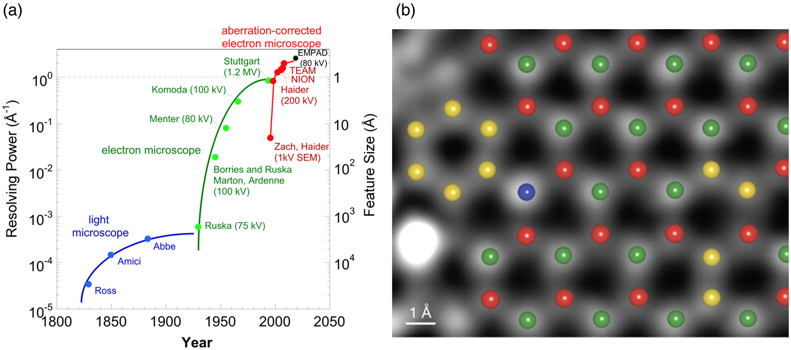
Fig. 1. (a) Hardware advances in resolving power of microscopes. (b) Atom-by-atom structural and chemical analysis by annular dark-field electron microscopy. Part of a density functional theory simulation of a single BN layer containing the experimentally observed substitutional impurities overlaid on the corresponding part of the experimental image. Boron in red; Carbon in yellow; Nitrogen in green; Oxygen in blue. (a) Adapted from Rose (Reference Rose2009) and Muller (https://devicematerialscommunity.nature.com/search?utf8=%E2%9C%93&query=muller). (b) Adapted from Krivanek et al. (Reference Krivanek, Chisholm, Nicolosi, Pennycook, Corbin, Dellby, Murfitt, Own, Szilagyi, Oxley, Pantelides and Pennycook2010a).
Development of the Scanning Transmission Electron Microscope
The Early Development
The invention of the fax machine by Alexander Bain is usually considered as the first use of forming images by a scanning system (Bain, Reference Bain1843; McMullan, Reference McMullan1990). To overcome the Abbe limit on the resolution of light microscopes, Synge applied the scanning method, by using a light probe with an aperture smaller than the wavelength of the light, to form scanned images (Synge, Reference Synge1928). Although there were no major breakthroughs in improving image resolution, Synge proposed the use of piezo-electric actuators, the formation of a visible image on a phosphor screen, and the image contrast expansion by processing electronic signals (Synge, Reference Synge1928, Reference Synge1931, Reference Synge1932). All these early proposals have been effectively utilized for developing the state-of-the-art scanning microscopes. Stintzing filed a patent for a proposed scanning microscope to be capable of automatic detection and measurement of particles using a light or electron beam (Stintzing, Reference Stintzing1929; McMullan, Reference McMullan1989). Since the possibility of focusing electrons was not known at that time, Stintzing proposed the use of crossed slits to form small diameter light or electron probes (McMullan, Reference McMullan1989). No practical scanning microscopes were constructed to demonstrate the feasibility of these scanning imaging systems.
Soon after the construction of the first transmission electron microscope (TEM), Max Knoll started working on television camera tubes and developed an electron-beam scanner for observing the targets of these tubes. Knoll was the first to publish images obtained by scanning an electron beam (Knoll, Reference Knoll1935). The electron-beam scanner that Knoll constructed, with electron energies in the range of 500–4,000 eV, possessed all the principal features of a modern scanning electron microscope (SEM). Knoll demonstrated that the image magnification of an SEM could be controlled by varying the ratio of the scan amplitudes: with a fixed display size, the smaller the scanned area, the higher the image magnification. Such an understanding of magnification of scanned images was also realized by the television and electron microscope pioneer Zworykin (Zworykin, Reference Zworykin1934; Zworykin et al., Reference Zworykin, Hillier and Snyder1942) who worked on a light microscope fitted with a TV camera. With the electron-beam scanner, Knoll investigated not only cathode-ray tubes but also other types of solid samples and determined the contrast mechanisms of his scanning images (Knoll, Reference Knoll1941; McMullan, Reference McMullan1995).
Manfred von Ardenne, an eminent applied physicist and prolific inventor, built the first STEM (Fig. 2a) with the goal to image thicker samples, which posed a major problem for TEM imaging due to chromatic effects, without degrading image resolution (McMullan, Reference McMullan1995). In a series of publications within a short period of time, von Ardenne described detailed analyses of the design and performance of probe-forming electron optics using magnetic lenses (von Ardenne, Reference von Ardenne1938a, Reference von Ardenne1938b, Reference von Ardenne1938c, Reference von Ardenne1939, Reference von Ardenne1940). He discussed the effects of lens aberrations on the probe size and how to calculate the current in an electron probe, showed how detectors should be placed for bright-field (BF) and dark-field (DF) STEM imaging, and considered the effects of electron beam and amplifier noise on image quality. With the use of a smaller electron probe for high-resolution imaging, the total electron-beam intensity within the electron probe was, however, drastically reduced, resulting in a long recording time to obtain each visually observable image. Since there were no suitable low-noise electronic detectors available at that time, photographic films had to be used to record reasonable quality STEM images. The long acquisition time to obtain each small-probe size STEM image imposed a fatal limitation on practical STEM imaging since one could not focus the electron probe properly without quickly examining the raster image. When large electron probe sizes, which provided higher probe current for rapid raster images, were used only low-resolution STEM images were obtained, offering no advantages over TEM. The lack of appropriate electron detectors and bright electron sources at that time severely limited the development and applications of high-resolution STEM. On the other hand, the high yield of low-energy secondary electrons and the development of the highly efficient Everhart-Thornley detector (Everhart & Thornley, Reference Everhart and Thornley1960) made it possible to obtain high-quality SEM images of surfaces of various types of samples, leading to the successful commercialization of the first SEM by the Cambridge Instrument Company (Oatley, Reference Oatley1982).
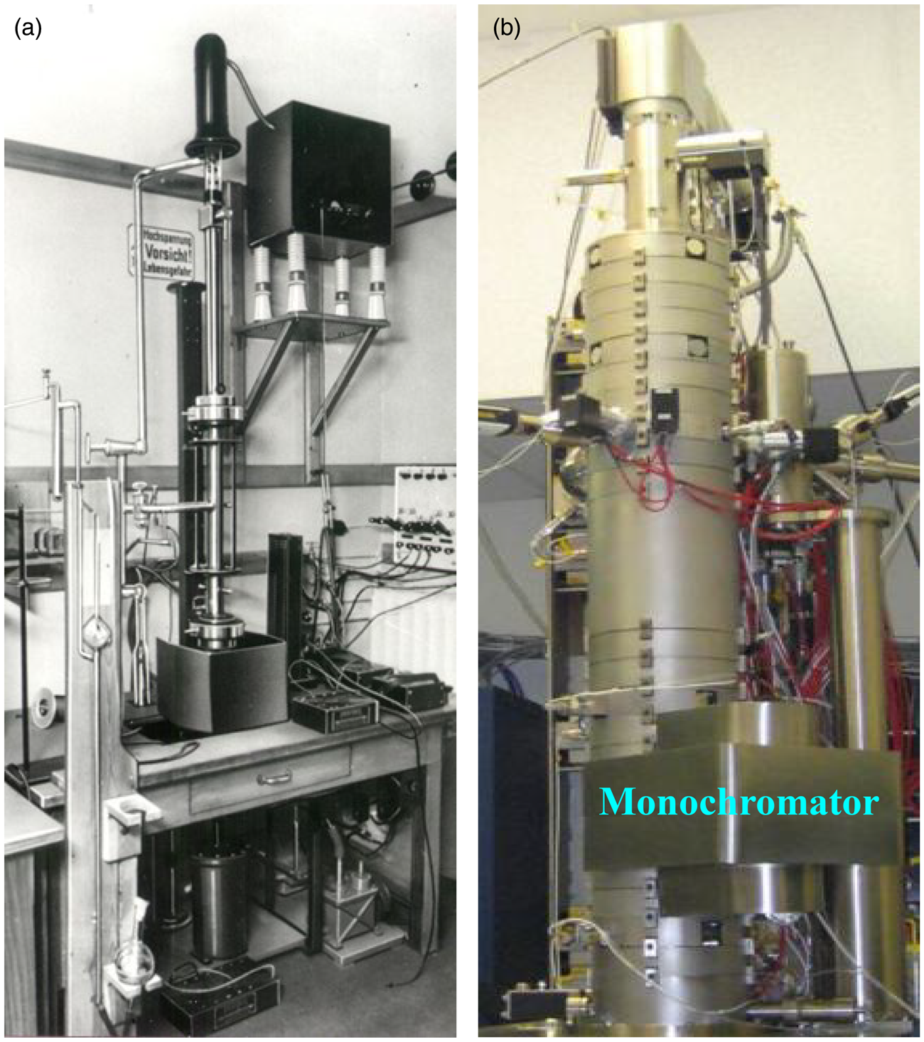
Fig. 2. (a) Manfred von Ardenne developed the first scanning transmission electron microscope (1938), with an electron-beam diameter on target of ~10 nm. His first image was a zinc oxide crystal at 8,000× magnification. Adapted from Science/AAAS Custom Publishing Office (http://poster.sciencemag.org/sem/#). (b) The Nion aberration-corrected and monochromated UltraSTEM 100 at Arizona State University: sub-Ångstrom resolution at 60/100 kV, about 1 Ångstrom resolution at 30/40 kV, and 10 meV energy solution in ultrafast EELS.
Albert Crewe's Field-Emission Scanning Electron Microscope
Crewe proposed a new type of scanning microscope in 1963 with the objective to overcome the barriers to improving image resolution by using electron beams (Crewe, Reference Crewe1963). In his 1966 paper, Crewe, after analyzing the probe-forming lenses of the SEM (Oatley et al., Reference Oatley, Nixon and Pease1965; Pease & Nixon, Reference Pease and Nixon1965), realized that the existing scanning microscopes were severely limited by electron source problems: The electron source brightness was too low and, therefore, it was not possible to de-magnify such an electron source to atomic size with any usable current (Crewe, Reference Crewe1966). Crewe realized the practicality of field emission from a small tungsten tip (Fowler & Nordheim, Reference Fowler and Nordheim1928; Dyke et al., Reference Dyke, Trolan, Dolan and Barnes1953; Martin et al., Reference Martin, Trolan and Dyke1960; Gomer, Reference Gomer1961; Butler, Reference Butler1966; Crewe et al., Reference Crewe, Eggenberger, Wall and Welter1968b) and proposed the use of such a tip as the electron gun to generate a high-brightness electron source. The current density from a cold field-emission gun (108–109 A/cm2 sr) could be orders of magnitude higher than that from a thermionic electron gun (<106 A/cm2) and the diameter of the virtual source could be managed to become less than 10 nm. The use of a field-emission gun (FEG) was expected to drastically reduce the electron probe size and consequently to improve the image resolution of both SEM and STEM. Crewe further proposed the design of a new microscope with the use of quadrupole lenses and estimated that an electron source size of 3 nm could be achievable. The new microscope needed to maintain an ultrahigh vacuum to stabilize electron emission, and the transmitted electrons could be detected by a high-speed scintillator photomultiplier system. The newly proposed STEM could be easily fitted with an electrostatic spectrometer (Hillier & Baker, Reference Hillier and Baker1944) for analyzing the energy of the transmitted electrons to enhance image contrast or to provide chemical contrast imaging. Since an ultrahigh vacuum was required, it was expected that contamination issues would not pose a significant problem on either image resolution and/or image contrast.
Crewe and colleagues (Crewe et al., Reference Crewe, Wall and Welter1968c) published the design of a simple STEM (Fig. 3a) and built an STEM with a field-emission electron source and one lens, providing high-contrast images with 3 nm resolution. The field-emission tip required a vacuum pressure below 10−9 Torr for stable operation. The power of using a tungsten field-emission tip was further demonstrated by the fact that even with the use of only the FEG and without the use of any focusing lenses, an image resolution of ~10 nm was obtained in transmission electron micrographs (Crewe et al., Reference Crewe, Isaacson and Johnson1969). The achievable electron probe current on the order of 100–10 pA, which allowed electron micrographs to be taken with scan times of 10 s, significantly improved from that of von Ardenne's STEM. The use of an FEG not only reduced the electron probe size but also drastically increased the probe current density, both of which enabled the attainment of high-resolution STEM images with a reasonable signal-to-noise ratio. The improved design and the astonishing performance of the new type of STEM, constructed by Crewe and his research group, were highlighted by the capability of directly observing single heavy atoms (Crewe & Wall, Reference Crewe and Wall1970; Crewe et al., Reference Crewe, Wall and Langmore1970). With the improved STEM design, Crewe and colleagues constructed a stronger cylindrically symmetrical magnetic lens (focal lengths of 0.6–1.0 mm) to reduce the spherical aberration coefficient (~0.4 mm); incorporated an annular detector (Cosslett, Reference Cosslett1965) to enhance the image contrast of different elements and to further improve signal strength; and attached an electrostatic electron spectrometer (0.3 eV resolution with 25 keV primary electron beam) to collect transmitted electrons with specific energies. The unique features of the new STEM as well as discussions on the various parameters that affect the final probe size were presented (Crewe & Wall, Reference Crewe and Wall1970). Since the probe-forming lens and the electron gun were rigidly connected together, the only alignment of the optical system was to make sure that the field-emission tip was placed on the optical axis of the microscope system and that the tip emission cone would not change during operation. The authors realized that, in strong contrast to conventional TEM, the electron probe current and the collected signal strength were independent of image magnification. Since the signal strength did not change with the image magnification, one could operate the STEM at high image magnifications (up to 5 × 10⁶). The Crewe's research group also realized that “phase contrast can be obtained by using a large aperture above the specimen and very small aperture below the specimen.”
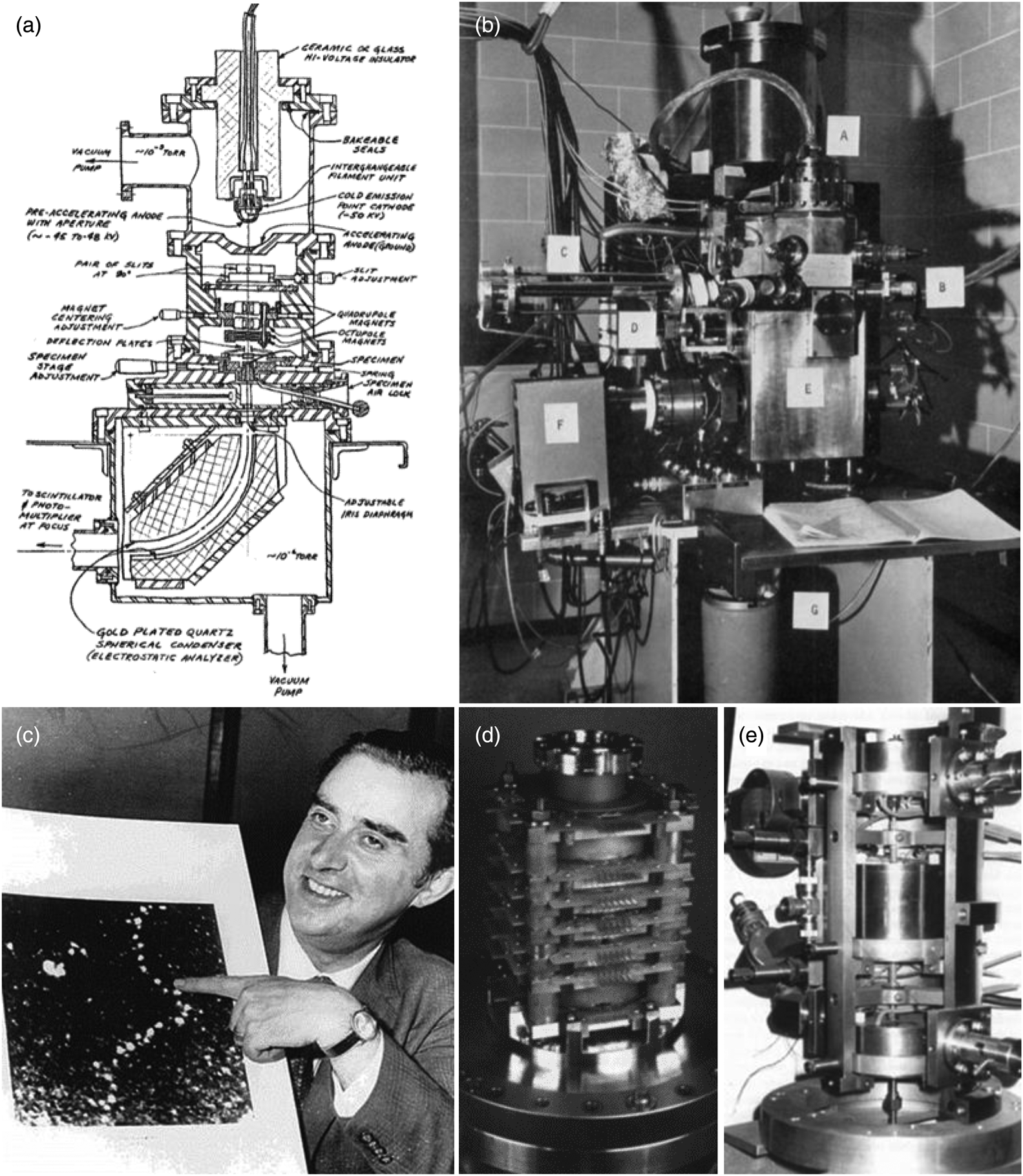
Fig. 3. Albert Crewe's first STEM design (a), the 0.5 nm STEM instrument (b), a chain of thorium atoms imaged on his STEM (c), the quadrupole–octupole corrector (d), and the sextupole corrector (e). Retrieved from https://www.microscopy.org/images/posters/Crewe.pdf.
Even with a 0.5 nm electron probe at 25 kV (Fig. 3b), Crewe and colleagues were able to visualize individual heavy atoms supported on ultrathin carbon films (Crewe et al., Reference Crewe, Wall and Langmore1970). They obtained two types of STEM images by collecting scattered electrons with an annular detector (excluding the directly transmitted electrons) and inelastically scattered electrons (passing through the hole of the annular detector) by the electron spectrometer. The ratio of these two images was expected to reduce the dependence of image contrast on thickness variations of the supporting carbon film, resulting in contrast enhancement of heavy atoms. Through detailed analyses and comparison of the experimentally measured visibility factors to those of theoretical calculations for carbon-supported uranium and thorium atoms, the authors concluded that the bright spots in their STEM images represented those of individual uranium or thorium atoms. To further corroborate their conclusion of visualizing individual heavy atoms, special samples, which consisted of isolated atom pairs, were prepared and examined. The experimentally obtained images matched the geometric patterns that were expected from the respective molecules supported on ultrathin carbon films. This was the first time ever to achieve the goal of directly imaging individual atoms with an electron microscope, and therefore, the FEG STEM surpassed the capability of conventional TEM for imaging individual heavy metal atoms (Fig. 3c; Crewe et al., Reference Crewe, Wall and Langmore1970). Four main factors accounted for imaging individual heavy atoms with a probe size of ~0.5 nm: (1) the high-current density of the FEG, (2) the large distances between the heavy atoms, (3) the strong heavy-atom contrast, and (4) the ultrathin carbon support which significantly reduced the strength of the background signal. The strong heavy-atom contrast originated from the ratio signal which strongly depended on the atomic number “Z” of the individual heavy atoms (Crewe, Reference Crewe1971). Therefore, by processing different categories of transmitted electrons to form new images, one could enhance elemental differentiation of the samples of interest, especially for heavy metal atoms or clusters supported on amorphous, light-element thin films. With the capability of analyzing inelastically scattered electrons, Crewe and colleagues (Crewe et al., Reference Crewe, Isaacson and Johnson1971a, Reference Crewe, Isaacson and Johnson1971b) studied the interactions of fast electrons with biological molecules and measured the corresponding energy-loss spectra of various nucleic acid bases. They further studied the potential of utilizing the energy-loss signal to enhance image contrast of biological specimens and investigated the phenomena of electron-beam-induced radiation damage and provided a measure of these effects.
With further improvement of the STEM design, operating at relatively higher electron-beam energies, and collecting elastically scattered electrons with an annular dark-field (ADF) detector, not only individual heavy atoms were imaged, but also atomic columns of small crystallites of uranium and thorium compounds were resolved (Wall et al., Reference Wall, Langmore, Isaacson and Crewe1974b). Furthermore, the authors used line intensity profiles of individual mercury atoms to estimate the finely focused electron probe size and demonstrated a full width at half maximum (FWHM) of 0.25 ± 0.02 nm at 42.5 kV with a total electron flux of 107 electrons/Å2. Since the signal-to-noise ratio available from a single heavy atom on a carbon support would increase with improvement of instrumental resolution, the authors proposed that higher electron-beam voltages (e.g., 100 kV) and a smaller probe size (e.g., <0.2 nm) would allow sufficient signal-to-noise for directly visualizing single atoms over more than half of the periodic table (Crewe, Reference Crewe1974; Wall et al., Reference Wall, Isaacson and Langmore1974a, Reference Wall, Langmore, Isaacson and Crewe1974b). By this time, the use of an FEG for STEM imaging had been unambiguously proved successful, especially for applications in imaging biological systems stained with heavy metal atoms or clusters.
The flexibility of STEM detectors, together with the capability of performing electron energy-loss analysis of transmitted electrons, provided a new approach to quantitatively evaluating mass thickness and composition of biological structures on a nanometer scale. The ADF imaging method was extensively used to determine the molecular masses of macromolecular assemblies and to visualize isolated protein assemblies via heavy metal labeling, leading to broad STEM applications in biology (Crewe, Reference Crewe1971; Wall & Hainfeld, Reference Wall and Hainfeld1986; Hainfeld, Reference Hainfeld1987; Colliex & Mory, Reference Colliex and Mory1994; Thomas et al., Reference Thomas, Schultz, Steven and Wall1994; Sousa et al., Reference Sousa, Hohmann-Marriott, Aronova, Zhang and Leapman2008; Engel, Reference Engel2009; Sousa & Leapman, Reference Sousa and Leapman2012). The early applications of electron energy-loss spectroscopy (EELS) to biological systems (Crewe et al., Reference Crewe, Isaacson and Johnson1971a, Reference Crewe, Isaacson and Johnson1971b; Isaacson, Reference Isaacson1972; Isaacson & Johnson, Reference Isaacson and Johnson1975) spurred EELS nanoanalysis in cell biology, pathology, microbiology, histology, and other branches of biomedical sciences (Ottensmeyer & Andrew, Reference Ottensmeyer and Andrew1980; Leapman & Ornberg, Reference Leapman and Ornberg1988; Leapman & Andrews, Reference Leapman and Andrews1992; Leapman, Reference Leapman2003; Aronova & Leapman, Reference Aronova and Leapman2012).
The Emerging STEM Research and the Commercial Development of STEMs
The success of Crewe's new STEM and the progressive improvement of image resolution in conventional TEM, from crystal lattice imaging (Menter, Reference Menter1956; Dowell, Reference Dowell1963; Komoda, Reference Komoda1966; Allpress et al., Reference Allpress, Sanders and Wadsley1969) to structural imaging (Iijima, Reference Iijima1971; Cowley & Iijima, Reference Cowley and Iijima1972; Allpress & Sanders, Reference Allpress and Sanders1973), clearly galvanized the excitement for developing high-voltage, high-resolution electron microscopes. Cowley and Strojnik started designing and building a 600-kV transmission scanning electron microscope and reported the initial results of their effort (Cowley & Strojnik, Reference Cowley and Strojnik1968, Reference Cowley and Strojnik1969; Cowley, Reference Cowley1970; Cowley et al., Reference Cowley, Smith and Sussex1970). In designing this high-voltage STEM, they used two lenses to form a small electron probe and added deflection systems to manipulate scattered electrons in order to obtain decent electron diffraction patterns and to direct the scattered electrons into the electron spectrometer for EELS analysis. Cowley specifically emphasized the usefulness of simultaneously acquiring STEM images and diffraction patterns from small regions of interest, for example, from dislocations or other types of defects (Cowley, Reference Cowley1970). If the scanning electron probe was stopped at any point of interest, a diffraction pattern, originating from a region with an area equal to the resolution limit of the STEM, would be recorded. In addition to investigating various STEM imaging modes, Cowley and colleagues studied the dependence of electron diffraction from crystalline samples on the defocus of the electron probe and discussed the origin of the fine structures in the observed convergent beam electron diffraction disks (Cowley et al., Reference Cowley, Smith and Sussex1970; Smith & Cowley, Reference Smith and Cowley1971), similar to, but not exactly the same as, those reported for convergent beam electron diffraction (CBED) in conventional TEM (Cockayne et al., Reference Cockayne, Goodman, Mills and Moodie1967). Cowley reported that the nature of the observed diffraction patterns depended on the aperture size of the probe-forming lens and that the lens aberrations (e.g., spherical and chromatic aberrations) had an effect on the observed fine structures in the wide-angle CBED patterns. When the electron beam was out-of-focus shadow images of the specimen within the wide-angle CBED disks appeared. It is interesting to note that Cowley and colleagues, based on the high-penetration power of high-energy electrons and the fact that, in an STEM, no imaging lenses were needed after the sample, proposed designs for conducting electron microscopy imaging and diffraction experiments on samples that could be exposed to air or other types of gases (Cowley et al., Reference Cowley, Smith and Sussex1970). Cowley and Strojnik did not seem to consider the use of an FEG as the electron source. Even though they used high voltages and two lens systems to form the electron probe, the resolution of this high-voltage STEM was limited to ~1 nm.
Other research groups worldwide either proposed or started the construction of high-voltage electron microscopes with an expectation of approaching 0.1 nm image resolution, significantly extending the electron microscopes’ capabilities, especially for studies of biological systems. Such an enthusiasm of the electron microscopy research community was clearly reflected in a special Physics Today report (Lubkin, Reference Lubkin1974). Even the abstract of this special report described the excitement and the potential of high-resolution STEMs/TEMs as described below.
“Several groups are building electron microscopes with high voltage or high resolution or both that should distinctly extend their capabilities, particularly for observations in biology. One such group, which we recently visited at the Cavendish Laboratory, University of Cambridge, is building a 600-kV conventional microscope that is expected to have a resolving power approaching 1 Å, according to V. E. Cosslett and W. C. Nixon, who head the Cavendish team. Among those hoping to extend the frontiers of electron microscopy, besides the Cavendish, are groups at Oak Ridge National Laboratory, Cornell University, the University of Kyoto, the University of Nagoya, the University of Chicago and Arizona State University.”
Crewe's development and demonstration of the power of his high-resolution, field-emission STEM stimulated the commercial development of such electron microscopes. Komoda and his colleagues in Japan started constructing scanning electron microscopes similar to Crewe's microscope (Komoda & Saito, Reference Komoda and Saito1972; Komoda et al., Reference Komoda, Tonomura, Ohkura and Minamikawa1972). The constructed field-emission SEM could be used with accelerating voltages up to 50 kV with capabilities for STEM imaging as well as secondary electron imaging. The improved resolution in secondary electron imaging, due to the use of a smaller but high-current-density electron probe, eventually led to the successful development of the first commercialized cold FEG SEM in 1972. By 1975, Hitachi completed the design and development of a 50-kV cold FEG STEM which revealed 0.2 nm lattice spacings of Au in phase-contrast BF STEM images (Inada et al., Reference Inada, Kakibayashi, Isakozawa, Hashimoto, Yaguchi and Nakamura2009). Based on Peter Hawkes’ account (Hawkes, Reference Hawkes2009a, Reference Hawkes2009b), in addition to Vacuum Generators, two other companies, AEI (Associated Electrical Industries) of Britain and Siemens of Germany, constructed STEMs in the early 1970s. By 1973, the AEI STEM provided an image resolution of ~1.0 nm and could operate at 80 kV. Later, prototype AEI STEMs improved the image resolution to ~0.3 nm and lattice spacings of ~0.2 nm were discernible. The Siemens FEG STEM could operate from 10 to 100 kV and electron deflection systems both before and after the specimen were incorporated to adjust the electron beam to allow proper detection of scattered electrons by the imaging detectors/electron analyzer and to permit recording of diffraction patterns. The Siemens STEM demonstrated the employment of large bright-field detectors and ADF detectors to suppress phase contrast of biological samples.
Vacuum Generators (VGs), established to meet the demand of ultrahigh vacuum-based technologies, already started building low-energy electron diffraction (LEED) systems, Auger electron spectrometer systems, and X-ray photoelectron spectrometer (XPS) systems in the late 1960s and early 1970s. Since VG specialized in ultrahigh vacuum (UHV) chambers and had developed stable field-emission sources for commercial instruments (Lilburne et al., Reference Lilburne, Herd and Stuart1970), it was a natural fit for VG to move forward producing high-voltage and high-resolution UHV-based STEMs. VG established a microscope division by 1972 to produce commercial STEMs (Wardell & Bovey, Reference Wardell and Bovey2009). The VG research team optimized all the relevant components of a dedicated commercial STEM (e.g., strongly excited asymmetrical objective lens, top entry specimen stage and cartridge, and so on). The design strategy for the objective lens followed Cowley's reciprocity principle between TEM and STEM (Cowley, Reference Cowley1969). The VG researchers especially emphasized the huge potential of incorporating analytical systems and post-specimen lens systems to the main microscope column and therefore decided to put the cold FEG at the bottom of the microscope column. By 1974, VG already delivered two dedicated STEMs (codenamed as HB5 of which HB refers to high-brightness electron gun) that could operate at 100 kV with a specified image resolution of ~0.5 nm and these dedicated STEMS could resolve the 0.34 nm lattice fringes of graphite in the BF STEM imaging mode (Wardell et al., Reference Wardell, Morphew and Bovey1973; Wardell & Bovey, Reference Wardell and Bovey2009). By working together with the STEM users, VG continuously improved the performance of the HB5 STEM, soon obtaining 0.144 nm Au lattice fringes. The later versions of the HB5 incorporated a windowless X-ray detector, a virtual objective aperture, an improved electron energy-loss spectrometer, a diffraction pattern observation screen, and so on (Wardell & Bovey, Reference Wardell and Bovey2009). By integrating many of the progressive improvements that were practiced on the HB5 STEMs, VG introduced in 1981 a new model HB501 as a high-performance analytical electron microscope. In the late 1980s, the demand for atomic-resolution imaging expedited the development of the 100-kV HB501UX with a stronger objective lens, reaching an image resolution of ~0.22 nm in the ADF imaging mode. The VG HB601, commercialized in the 1990s, incorporated all the available digital systems and new detector technologies.
VG also produced specialized STEM instruments including the Microscope for Imaging, Diffraction and Analysis of Surfaces (MIDAS) at Arizona State University (Fig. 4) (Venables et al., Reference Venables, Cowley and von Harrach1987; von Harrach, Reference von Harrach2009). The MIDAS was a fully integrated UHV system including the microscope column, the sample preparation and transfer systems, the optical spectroscopy characterization systems, and gas exposure chambers. One of the unique designs of MIDAS involved the insertion of “parallelizer” coils in the objective lens bores, both before and after the specimen position (Kruit & Venables, Reference Kruit and Venables1988). The use of the “through-the-lens” design significantly increased the detection efficiency of Auger and secondary electrons. The MIDAS design increased the resolution of Auger electron imaging from tens of nanometers to below 1 nm. Such a surface and elemental sensitive imaging technique was applied to investigations of industrial bimetallic catalysts, with an expectation of extracting information about the effects of catalyst surface segregation on heterogeneous catalysis. For studies of in situ deposited Ag nanoclusters, detection of <10 Ag atoms by Auger analysis was accomplished (Liu et al., Reference Liu, Hembree, Sinnler and Venables1992, Reference Liu, Hembree, Sinnler and Venables1993a). Based on the design and construction of the MIDAS, VG started designing and constructing 300-kV STEMs (von Harrach, Reference von Harrach2009), denoted as HB603, with excellent analytical capabilities (Lyman et al., Reference Lyman, Goldstein, Williams, Ackland, Von Harrach, Nicholls and Statham1994; von Harrach, Reference von Harrach1994; Watanabe & Williams, Reference Watanabe and Williams1999). The VG HB603 U was developed for ultrahigh image resolution (von Harrach et al., Reference von Harrach, Nicholls, Jesson and Pennycook1993; von Harrach, Reference von Harrach1994). Unfortunately, the VG Microscopes Ltd. stopped operation in May 1996, just a few years prior to the broad acceptance of the power of STEMs by scientific research communities.
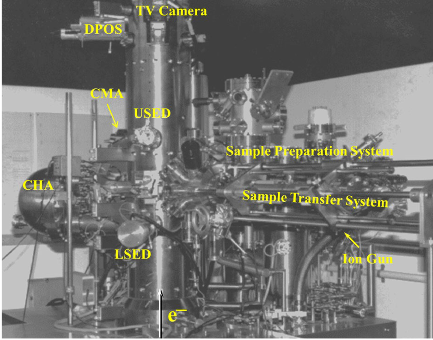
Fig. 4. Arizona State University's MIDAS (Microscope for Imaging, Diffraction and Analysis of Surfaces).
The sudden stop of the production of dedicated STEMs by VG Microscopes shocked the elite community who relied on VG dedicated STEMs to conduct their research. Nigel Browning of the University of Illinois–Chicago, who had planned to purchase a VG dedicated STEM for his research programs, could not find a supplier of dedicated STEMs. Although FEG TEMs were readily available from electron microscope vendors, there were no reports, however, on achieving atomic-resolution ADF STEM images on such FEG TEMs. By working with the JEOL company to slightly modify an FEG JEOL 2010F (200 kV) to produce a small electron probe and to collect electrons scattered to high angles, Browning and colleagues (James et al., Reference James, Browning, Nicholls, Kawasaki, Xin and Stemmer1998) were able to demonstrate a sub-2 Å resolution in high-angle ADF (HAADF) images. These impressive results manifested that a commercial FEG TEM could be operated as an STEM and could provide atomic-resolution STEM images comparable to those that achieved at 300 kV on the VG HB603 U dedicated STEM. In a subsequent paper, James & Browning (Reference James and Browning1999) conducted a full investigation on how to obtain small electron probes for STEM imaging on a high-performance FEG TEM. They further demonstrated that all the capabilities achievable on a dedicated STEM could be accomplished on an FEG TEM except that with a Schottky-emission electron gun, the energy resolution of the acquired EELS spectra was not as good as that obtained on a cold FEG dedicated STEM. The demonstration of achieving atomic-resolution STEM imaging on a conventional 200-kV FEG TEM with a Schottky-emission electron gun had important implications and, to a large degree, accelerated the adoption of atomic-resolution STEM imaging and the associated techniques by broad scientific research communities. The quick acceptance of atomic-resolution Z-contrast imaging on FEG TEMs, the significant reduction of instabilities due to microscope and/or environmental factors, and the realization of aberration-correction to form sub-Å electron probes all expedited the broad applications of atomic-resolution STEM in solving challenging materials problems.
The Era of Aberration-Corrected STEM
Unlike light microscopes, electron microscopes suffer from the unavoidable, positive spherical aberration of rotationally symmetric electron lenses regardless of skillful lens design and perfect fabrication (Scherzer, Reference Scherzer1936). Scherzer pointed out that by considering alternative approaches, drastically different from axially symmetric round lenses, it would be possible to correct electron lens aberrations (Scherzer, Reference Scherzer1947). Tremendous efforts were devoted to searching designs of lens and aberration correctors that would provide controllable and/or diminishing aberrations (Hawkes, Reference Hawkes1980, Reference Hawkes2009a, Reference Hawkes2009b, Reference Hawkes2015; Rose, Reference Rose2009; Marko & Rose, Reference Marko and Rose2010; Septier, Reference Septier2017). Soon after the FEG STEM was in operation, Crewe and colleagues started designing and developing aberration correctors with the goal of drastically reducing the effects of lens aberrations on limiting the STEM probe size (Crewe et al., Reference Crewe, Cohen and Meads1968a; Beck & Crewe, Reference Beck and Crewe1974; Beck, Reference Beck1979; Crewe, Reference Crewe1980, Reference Crewe1982, Reference Crewe1983a, Reference Crewe1983b, Reference Crewe1995, Reference Crewe2009; Crewe & Jiye, Reference Crewe and Jiye1985; Figs. 3d, 3e). Shao (Reference Shao1988) published a paper discussing the mechanisms of the generation of fifth-order aberrations in a sextupole-corrected electron optical system and proposed a new approach to compensating the rotationally symmetric part of fifth-order aberrations. Numerical simulations implied that by using an additional round lens, the electron probe radius could be reduced from 0.08 to about 0.04 nm for 200 keV electrons, achieving sub-Ångstrom resolution. On the experimental front, however, the progress was much more sluggish and frustrating. Crewe and colleagues tested the quadrupole/octupole corrector, introduced the concept of sextupole corrector, and other optical elements. Even with their tremendous effects (>30 years), however, they did not succeed in demonstrating practical resolution improvement (Crewe, Reference Crewe2004). In retrospect, many of the required tools for successfully diagnosing and auto-tuning the lens aberrations had not been developed. In addition to innovative optical designs, faster computers, robust testing algorithms, high-quality electronic devices, and high-precision lens fabrication skills are all required for the successful development of practical aberration correctors. Furthermore, as the STEM probe size became smaller and smaller stringent requirements for microscope and environment stability might have imposed another limiting factor on achieving sub-Å resolution imaging.
Zach and Haider (Reference Zach and Haider1994, Reference Zach and Haider1995a, Reference Zach and Haider1995b), based on a new design of a high-resolution low-voltage scanning electron microscope (Zach, Reference Zach1989), developed the first workable multipole corrector and clearly demonstrated resolution improvement, even for low-energy electron beams. By using a quadrupole/octupole corrector, they reduced both the spherical and chromatic aberration, allowing for a theoretical resolution limit of ~1 nm at electron-beam energies between 0.5 and 1 keV. They experimentally obtained an image resolution <2 nm at 1 keV. Haider et al. (Reference Haider, Braunshausen and Schwan1995), based on Rose's solution for spherical aberration-correction (Rose, Reference Rose1990), utilized two electromagnetic hexapoles and four additional lenses to construct a hexapole-corrector for a 200 kV TEM and experimentally demonstrated resolution improvement over the non-aberration-corrected TEM (Haider et al., Reference Haider, Uhlemann, Schwan and Kabius1997, Reference Haider, Uhlemann, Schwan, Rose, Kabius and Urban1998). These astonishing achievements firmly established the practicality of incorporating aberration correctors into TEMs to significantly improve image resolution.
In a parallel development, Krivanek and colleagues constructed a quadrupole/octopole corrector equipped with computer control which could make numerous adjustments rapidly and systematically. They incorporated this corrector into a dedicated STEM instrument and were able to produce smaller electron probes by increasing the size of the illumination aperture which also allowed more electrons passing through the lens (Krivanek et al., Reference Krivanek, Dellby, Spence, Camps and Brown1997a, Reference Krivanek, Dellby, Spence, Camps and Brown1997b). In their subsequent work, Krivanek et al. (Reference Krivanek, Dellby, Spence and Brown1998) showed a Ronchigram with the radius of the flat phase disk extending to ~15 mrad which was ~2× larger than that of the uncorrected STEM instrument, unambiguously demonstrating the correction of spherical aberration to produce smaller probe sizes. The BF STEM images showed a reduced delocalization effect as well. Krivanek et al. (Reference Krivanek, Dellby and Lupini1999) presented the design of a second-generation quadrupole–octupole CS corrector to compensate high-order parasitic aberrations and predicted that sub-Ångstrom electron probes should be achievable at 100 kV when system instabilities were significantly reduced. In this new design, the fifth-order geometrical aberrations of the combination of corrector and probe-forming lens were expected to be eliminated. By 2001, impressive experimental results were obtained at 100 kV with an image resolution of ~123 pm in ADF STEM images (Dellby et al., Reference Dellby, Krivanek, Nellist, Batson and Lupini2001). By 2002, Batson et al. (Reference Batson, Dellby and Krivanek2002), by integrating a second-generation STEM corrector to an old VG HB501 STEM (120 kV), obtained impressive ADF images of gold atoms with a measured width of ~80 pm. This result unambiguously demonstrated the power of aberration-corrected STEM and its huge potential for materials characterization at sub-Ångstrom level with low-energy electrons. Krivanek's STEM corrector demonstrated an image resolution of 78 pm at 300 kV, clearly resolving the close-packed Si444 atomic spacing with the electron beam along the Si [112] zone axis (Nellist et al., Reference Nellist, Chisholm, Dellby, Krivanek, Murfitt, Szilagyi, Lupini, Borisevich, Sides and Pennycook2004).
Haider et al. (Reference Haider, Uhlemann and Zach2000) discussed the upper limits for the residual aberrations to form desired probe sizes and provided guidance on selecting appropriate parameters that control corrector alignment and diagnosis. Krivanek et al. (Reference Krivanek, Nellist, Dellby, Murfitt and Szilagyi2003) described a new design of a quadrupole/octupole corrector to correct all fifth-order aberrations while still keeping a small CC value. They proposed that when such a corrector is coupled to an optimized STEM column, sub-Ångstrom probe sizes would be obtainable at 100 kV and sub-0.5 Å probes would be achievable at higher operating voltages. In addition to reducing the electron probe size, the proposed STEM corrector could increase the total current available in an atom-size probe by a factor of 10 or more. Further refinements in aberration correctors, improvement in illumination source size and coherence, and microscope stability continuously improved the STEM image resolution to 63 pm in 2007 (Sawada et al., Reference Sawada, Hosokawai, Kaneyama, Ishizawa, Terao, Kawazoe, Sannomiya, Tomita, Kondo, Tanaka, Oshima, Tanishiro, Yamamoto and Takayanagi2007), 47 pm in 2009 (Erni et al., Reference Erni, Rossell, Kisielowski and Dahmen2009; Sawada et al., Reference Sawada, Tanishiro, Ohashi, Tomita, Hosokawa, Kaneyama, Kondo and Takayanagi2009), ~45 pm in 2015 (Sawada et al., Reference Sawada, Shimura, Hosokawa, Shibata and Ikuhara2015), and 40.5 pm in 2018 (Morishita et al., Reference Morishita, Ishikawa, Kohno, Sawada, Shibata and Ikuhara2018). Figure 5 shows the comparison of a pair of HAADF-STEM images obtained before and after aberration-correction, demonstrating the power of aberration-corrected STEM in characterizing nanostructured catalysts (Nellist & Pennycook, Reference Nellist and Pennycook1996; Pennycook, Reference Pennycook2017). Figure 6 displays a series of images (with an acquisition time of 4 s per frame) obtained sequentially to track the diffusion path of Ce dopant in the w-AlN single crystal (Ishikawa et al., Reference Ishikawa, Lupini, Findlay, Taniguchi and Pennycook2014). The Al–N “dumbbells” are clearly resolved and the brighter columns represent the Al sites. The brightest column, indicated by the white arrowhead, contained a single Ce dopant, moving to a different location in each image panel. By detailed image analyses and simulations, the authors deduced that these observations strongly suggested vacancy-, and occasionally, interstitial-mediated diffusion in Ce-doped w-AlN. Although the Ce diffusion was driven by the electron-beam-induced effects, such a method could be applicable for studying diffusion mechanisms in other materials systems with diffusion barriers such that the transition times are comparable to the scan rate of the STEM.
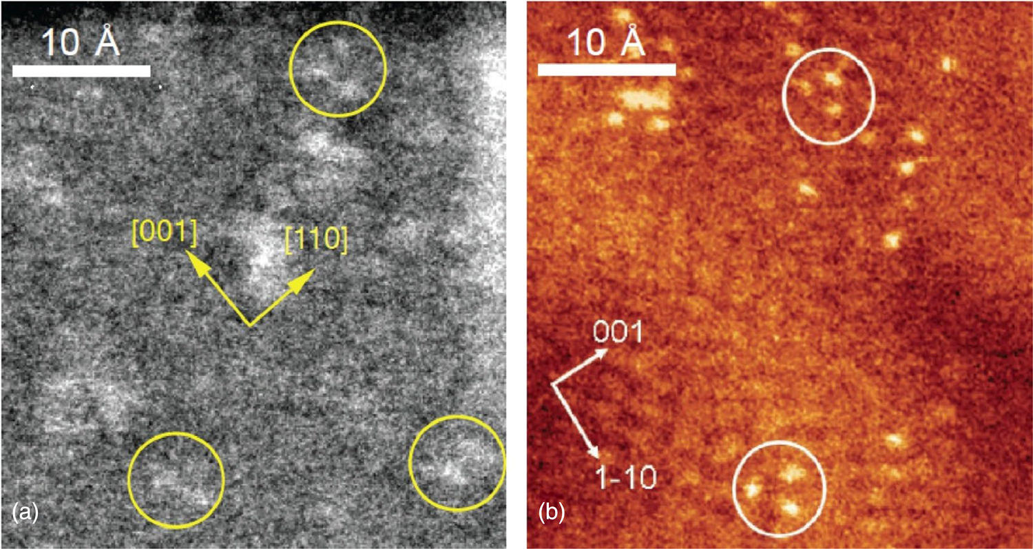
Fig. 5. Imaging of Pt atoms on γ-alumina with a VG Microscopes HB603 U 300 kV STEM (a) before and (b) after aberration-correction. Some Pt trimers and dimers are just visible in (a) but individual atoms and clusters are much clearly visualized in (b). Reproduced from Pennycook (Reference Pennycook2017).
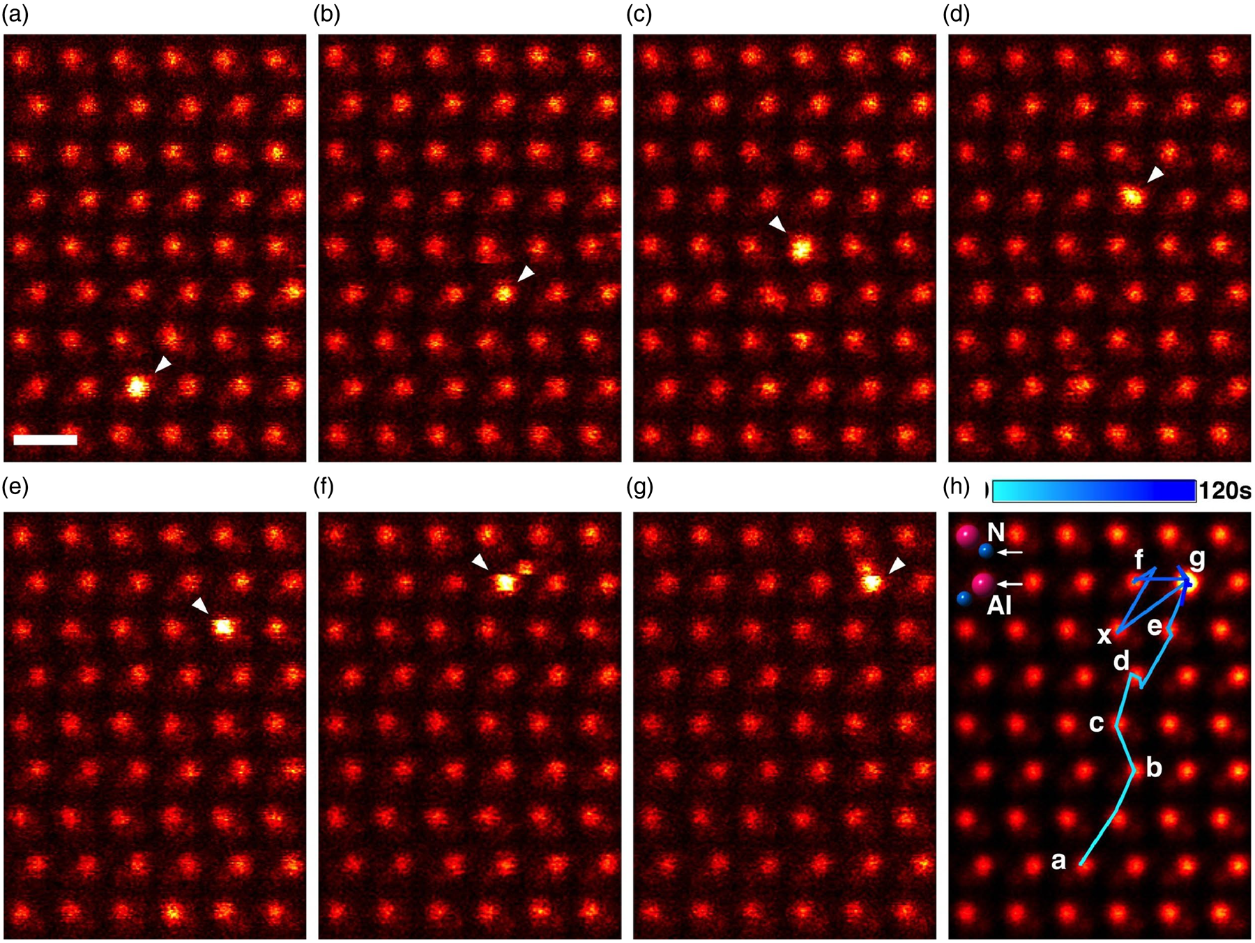
Fig. 6. Selected frames from a sequence of 30 Z-contrast images of a w-AlN single-crystal doped with Ce viewed along the [11–20] zone axis. (a–g) Frames 1, 4, 5, 6, 10, 16, 20, respectively, show the locations of a single Ce dopant as marked by the arrowhead in each panel. (h) Frame-averaged Z-contrast image. The observed Ce trace is overlaid and the Ce positions in each panel (a–g) are indicated. The scale bar is 3 Å. Reproduced from Ishikawa et al. (Reference Ishikawa, Lupini, Findlay, Taniguchi and Pennycook2014).
Since electron-beam-induced knock-on damage depends on the primary electron energy, atomic-resolution STEM imaging at low voltages is critical to studying a variety of materials, especially 2D materials or carbon-based materials. After optimizing the conditions of the ac-STEM, Krivanek et al. (Reference Krivanek, Chisholm, Nicolosi, Pennycook, Corbin, Dellby, Murfitt, Own, Szilagyi, Oxley, Pantelides and Pennycook2010a) were able to obtain impressive ADF STEM images, at 60 kV, of monolayer BN sample with clear contrast differentiation between B and N atoms. These authors further demonstrated that they could differentiate B, C, N, and O atoms that were present in the BN sample (Fig. 1b). This work unambiguously demonstrated the potential of low-voltage atomic-resolution STEM for resolving and identifying atomic species in 2D materials systems. Atom-by-atom structural and chemical analysis of all radiation damage-resistant atoms present in, and on top of, ultrathin sheets became practical (Krivanek et al., Reference Krivanek, Chisholm, Nicolosi, Pennycook, Corbin, Dellby, Murfitt, Own, Szilagyi, Oxley, Pantelides and Pennycook2010a, Reference Krivanek, Dellby, Murfitt, Chisholm, Pennycook, Suenaga and Nicolosi2010b; Sasaki et al., Reference Sasaki, Sawada, Hosokawa, Kohno, Tomita, Kaneyama, Kondo, Kimoto, Sato and Suenaga2010; Dellby et al., Reference Dellby, Bacon, Hrncirik, Murfitt, Skone, Szilagyi and Krivanek2011; Suenaga et al., Reference Suenaga, Iizumi and Okazaki2011).
Another major development was the incorporation of monochromators for ultrahigh energy-resolution EELS. The electron analyzer was incorporated at the very beginning of STEM development to enable chemical analysis capabilities with high spatial resolution (Crewe et al., Reference Crewe, Isaacson and Johnson1971b; Colliex et al., Reference Colliex, Cosslett, Leapman and Trebbia1976). However, even with a cold FEG the energy resolution (~0.2–0.3 eV) is still too large compared with other broad beam techniques (e.g., Raman or infrared spectroscopy) and consequently vibrational excitations of matter could not be explored at high spatial resolution. The integration of a monochromator (Tsuno, Reference Tsuno2011; Kimoto, Reference Kimoto2014; Hawkes & Krivanek, Reference Hawkes and Krivanek2019) into an STEM instrument (Fig. 2b) drastically improved the energy resolution of STEM-EELS (Krivanek et al., Reference Krivanek, Ursin, Bacon, Corbin, Dellby, Hrncirik, Murfitt, Own and Szilagyi2009). An energy resolution of 30 meV was demonstrated with an atom-size electron probe, enabling both atomic-resolution STEM imaging and ultrahigh energy-resolution EELS (Krivanek et al., Reference Krivanek, Lovejoy, Dellby and Carpenter2013). The full potential of atomic-resolution monochromated STEM was realized and vibrational spectra from different systems with atom-size probes were reported (Krivanek et al., Reference Krivanek, Lovejoy, Dellby, Aoki, Carpenter, Rez, Soignard, Zhu, Batson, Lagos, Egerton and Crozier2014a), firmly establishing the practical applications of vibrational spectroscopy on an STEM instrument. Further improvement to an energy resolution of sub-10 meV on the Nion ac-STEM was proposed (Krivanek et al., Reference Krivanek, Lovejoy, Murfitt, Skone, Batson and Dellby2014b), and with optimization of electron optical and electronic systems, an energy resolution of ~4 meV was realized (Hachtel et al., Reference Hachtel, Huang, Popovs, Jansone-Popova, Keum, Jakowski, Lovejoy, Dellby, Krivanek and Idrobo2019; Krivanek et al., Reference Krivanek, Dellby, Hachtel, Idrobo, Hotz, Plotkin-Swing, Bacon, Bleloch, Corbin, Hoffman, Meyer and Lovejoy2019). Figure 7 schematically illustrates the configuration of the Nion monochromator and how it is incorporated into an aberration-corrected Nion STEM for ultrahigh energy-resolution experiments. It is anticipated that further improvement in energy resolution to sub-meV may become plausible.
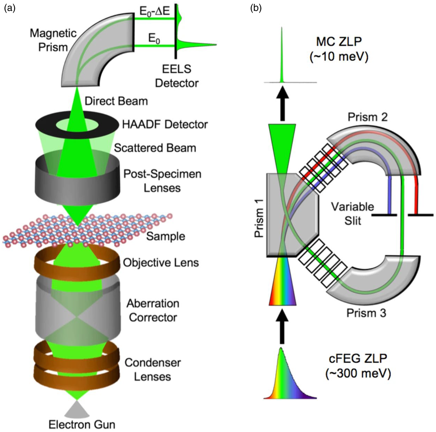
Fig. 7. Electron energy-loss spectroscopy and monochromation. (a) Schematic of electron energy-loss spectroscopy (EELS) experiment in a scanning transmission electron microscope (STEM). (b) Schematic of monochromation of electron beam (occurring between the electron gun and the condenser lenses). Reproduced from Hachtel et al. (Reference Hachtel, Lupini and Idrobo2018).
The integration of vibrational spectroscopy into the atomic-resolution STEM opened new opportunities for investigating the properties and functions of matter, and impressive results have already been published (Krivanek et al., Reference Krivanek, Lovejoy, Dellby, Aoki, Carpenter, Rez, Soignard, Zhu, Batson, Lagos, Egerton and Crozier2014a; Lagos et al., Reference Lagos, Trügler, Hohenester and Batson2017; Idrobo et al., Reference Idrobo, Lupini, Feng, Unocic, Walden, Gardiner, Lovejoy, Dellby, Pantelides and Krivanek2018; Hachtel et al., Reference Hachtel, Huang, Popovs, Jansone-Popova, Keum, Jakowski, Lovejoy, Dellby, Krivanek and Idrobo2019; Hage et al., Reference Hage, Kepaptsoglou, Ramasse and Allen2019; Senga et al., Reference Senga, Suenaga, Barone, Morishita, Mauri and Pichler2019). The possibility of atomic-resolution phonon mapping was proposed (Lugg et al., Reference Lugg, Forbes, Findlay and Allen2015a; Dwyer, Reference Dwyer2017; Hage et al., Reference Hage, Kepaptsoglou, Ramasse and Allen2019) and practically realized by Venkatraman et al. (Reference Venkatraman, Levin, March, Rez and Crozier2019) (Fig. 8), although the fundamental localization mechanisms and image contrast still need to be carefully evaluated (Hage et al., Reference Hage, Ramasse and Allen2020b; Rez & Singh, Reference Rez and Singh2021). Hage et al. (Reference Hage, Radtke, Kepaptsoglou, Lazzeri and Ramasse2020a) demonstrated the detection of distinctive localized vibrational signatures from a single-atom impurity in a solid (Si atom in graphene), clearly demonstrating single-atom sensitivity by STEM vibrational spectroscopy and inviting intriguing implications across the fields of physics, chemistry, and materials science. It is expected that with further development of novel electron detectors (Plotkin-Swing et al., Reference Plotkin-Swing, Corbin, De Carlo, Delby, Hoermann, Hoffman, Lovejoy, Meyer, Mittelberger, Pantelic, Piazza and Krivanek2020), atomic-resolution STEM-EELS, including vibrational spectroscopy, will significantly impact many research fields such as energy, nanoscience, and quantum science.
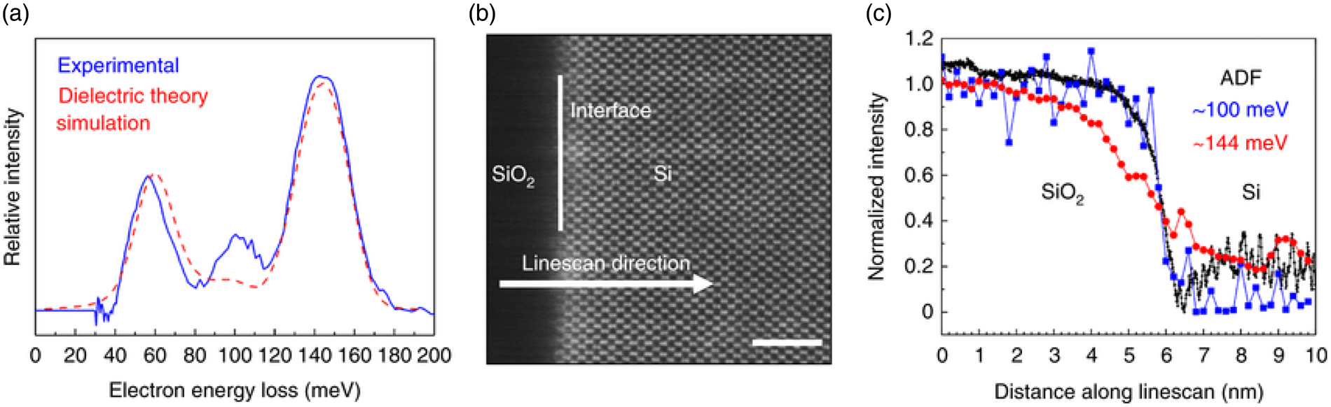
Fig. 8. High-resolution vibrational spectroscopy in SiO2. (a) Experimental energy-loss spectrum in SiO2 far from the interface (solid blue line) and a dielectric theory simulation of the spectrum (dashed red line). The peak at ~100 meV does not appear strongly in the dielectric simulation, indicating that it is predominantly excited by impact scattering. (b) Atomic-resolution ADF image of the SiO2/Si interface (showing the linescan direction across the interface). Scale bar = 2 nm. (c) Normalized signal profiles across the interface-100 meV (blue) and 144 meV (red)—overlaid on the contrast-reversed ADF signal profile. The 100 meV signal traces the ADF signal profile, thereby demonstrating high spatial resolution. Reproduced from Venkatraman et al. (Reference Venkatraman, Levin, March, Rez and Crozier2019).
The Development of STEM Imaging Theory
The Reciprocity Principle
When a crystalline specimen was examined, STEM images revealed diffraction effects such as Fresnel fringes, phase-contrast effects, and lattice fringes, which represented common features of conventional TEM images (Cowley & Strojnik, Reference Cowley and Strojnik1968, Reference Cowley and Strojnik1969; Crewe et al., Reference Crewe, Wall and Welter1968c; Cowley, Reference Cowley1969). To understand such STEM image contrast, Cowley (Reference Cowley1969) invoked the reciprocity principle, which had been previously discussed to link electron diffraction and imaging in conventional TEM (Pogany & Turner, Reference Pogany and Turner1968), to explain the diffraction and phase contrast in STEM images. By applying the reciprocity principle, Cowley concluded that “the image contrast of the STEM may be interpreted by direct analogy with the CTEM (conventional TEM) and the whole associated body of imaging theory will apply, the only variations being those depending on the geometry and special features of individual instruments.” Based on the symmetry of the Green's function formulation (Pogany & Turner, Reference Pogany and Turner1968), the reciprocity principle applies to multiple scattering events as well. Pogany and Turner stated that an approximate reciprocity relationship also held for inelastically scattered electrons provided that the change in energy and wave vector would be small enough. Further discussions on the reciprocity principle and its relationship to contrasts in STEM images can be found in papers published by Zeitler & Thomson (Reference Zeitler and Thomson1970a, Reference Zeitler and Thomson1970b).
In practice, the electron sources and detectors are not point objects but possess finite sizes which introduce the equivalence of coherent conditions in the corresponding configurations of CTEM and STEM, respectively. Since there are no imaging lenses, in an STEM, after the specimen the displayed pixel intensity of an STEM image should be proportional to the total number of electrons that are collected by the specific STEM detector. Therefore, the total signal strength collected by an STEM detector is the summation of the electron intensity (not wavefunction amplitude!) over all the detector pixels: The size, shape, and the position of the STEM detector with respect to the optical axis of the incident electron beam become critically important for interpreting the observed image contrast. If an STEM disk detector is positioned at the optical axis and subtends a convergent semi-angle α at the specimen then, by reciprocity, the equivalent TEM image should be formed with a condenser aperture that subtends the same convergent semi-angle α at the specimen, but this aperture should be incoherently illuminated. Therefore, BF STEM images obtained with larger detector sizes should have reduced phase contrast, analogy to the CTEM phase-contrast images obtained with large condenser apertures and incoherent illuminations. On the other hand, parallel illumination in the TEM generates coherently diffracted beams at the exit surface of the specimen. The equivalent condition for STEM imaging requires electron coherence across the hole of the STEM probe-forming aperture and the use of an infinitely small BF detector. The small size, cold FEGs satisfy the coherent requirement, resulting in small electron probes at the specimen provided that the effects of spherical and chromatic aberrations on the probe size are minimized. From this perspective, one can control the degree of phase contrast in BF STEM images by manipulating the effective size of the BF STEM detector.
Imaging Heavy Metal Atoms on Ultrathin Amorphous Films by the ADF Detector
The demonstration of ADF STEM imaging of isolated heavy atoms by Crewe and colleagues clearly attracted attention from the electron microscopy community and broader scientific research communities. From an electron scattering perspective, the bright contrast of heavy atoms supported on thin carbon films or decorating biological molecules seems intuitively understandable: the light-element thin support film does not scatter many of the incident electrons into the ADF detector while heavy atoms do. By collecting all the electrons scattered out of the incident electron illumination cone, high-quality atomic-resolution images enabled studies of diffusion processes of heavy atoms (Isaacson et al., Reference Isaacson, Kopf, Utlaut, Parker and Crewe1977). The direct visualization of diffusion of individual uranium atoms adsorbed onto a thin carbon film was thus realized. After careful evaluation of electron-beam-induced effects, the authors concluded that the observed motion of metal atoms was not caused by the impinging high-energy electrons. Since the primary electron-beam energies that were used to image supported metal atoms were relatively low, the knock-on damage, by the primary electrons, on both the carbon films and the metal atoms was most probably suppressed. However, other types of electron-beam-induced effects could not be completely ruled out, especially when the heavy metal atoms were not strongly anchored onto the support films.
The image contrast of supported metal atoms was evaluated by theoretical calculations and the results were compared to experimental data (Langmore et al., Reference Langmore, Wall and Isaacson1973; Retsky, Reference Retsky1974; Wall et al., Reference Wall, Isaacson and Langmore1974a, Reference Wall, Langmore, Isaacson and Crewe1974b; Beck & Crewe, Reference Beck and Crewe1975; Crewe, Reference Crewe1979, Reference Crewe1983a). These calculations illustrated the effects of electron probe size and atom size on the observed image resolution and intensities. Retsky's results clearly revealed quantization of the observed image intensities corresponding to one or two uranium atoms, suggesting that the experimentally acquired ADF images might represent incoherent imaging. With detailed analyses of image intensity profiles, differentiation of isolated Pt atoms from Pd atoms was also accomplished by collecting all the scattered electrons (Isaacson et al., Reference Isaacson, Kopf, Ohtsuki and Utlaut1979). In these early studies, most of the substrates were amorphous films and the metals were either single atoms or small clusters. Electron diffraction and channeling effects, which are usually present in STEM images of crystalline substrates or larger metal particles, did not play a dominant role, enabling a clear identification of single metal atoms with high image contrast. With this type of ideal samples, even though the inner collection angle of the ADF detector was small, the contrast of heavy atoms in ADF STEM images was intuitively interpretable. Although imaging of isolated metal atoms, and even their dynamic movement, were accomplished on these early atomic-resolution STEM instruments, practical applications of these atomic-resolution imaging methods to characterizing practical materials, frequently polycrystalline in nature and relatively thick, were not realized until much later.
Atomic Number (Z) and Phase-Contrast STEM Imaging
The Need for Reliably Identifying Supported Metal Clusters and Particles
The STEM images obtained by collecting all electrons scattered out of the primary electron illumination cone with a low-angle ADF detector demonstrated atomic number (Z)-dependent contrast for heavy metal atoms and clusters supported on thin carbon films (Crewe et al., Reference Crewe, Wall and Langmore1970, Reference Crewe, Langmore, Isaacson, Siegel and Beaman1975). Dividing the ADF signal by the simultaneously acquired signal of inelastically scattered electrons was expected to yield an interpretable Z-contrast image without the complications arising from variations in sample thicknesses. When Treacy et al. (Reference Treacy, Howie and Wilson1978) used this method to characterize supported Pt and Pd catalysts, they discovered that strong diffraction contrasts, arising from Bragg reflections in the crystalline component phases of the sample, dominated both the EELS and the ADF signals, masking the expected Z-dependence image contrast of metal clusters and nanoparticles. These authors realized that by increasing the inner collection angle of the ADF detector >0.25/nm (~100 mrad for 100 keV electrons), the Z-dependence contrast of the noble metal nanoclusters with sizes as small as 0.5 nm was recovered. Howie (Reference Howie1979) immediately pointed out that at such high angles of scattered electrons, thermal diffuse scattering could be more prominent than the coherent Bragg scattering. Furthermore, electron-channeling effects could still persist since even backscattered electrons had demonstrated channeling effects (Coates, Reference Coates1967; Howie et al., Reference Howie, Lunington and Tomlinson1971; Spencer et al., Reference Spencer, Humphreys and Hirsch1972). Based on Howie's proposal, Treacy et al. (Reference Treacy, Howie, Pennycook and Mulvey1980) and Treacy (Reference Treacy1982) demonstrated the power of HAADF imaging of supported metal catalysts, especially small metal clusters that could not be easily detected by TEM or other types of STEM imaging modes. The use of the HAADF imaging method has become a standard tool for characterizing supported metal catalysts, especially small noble metal clusters, atomically dispersed metals, and even isolated individual metal atoms on practical catalyst supports (Treacy & Rice, Reference Treacy and Rice1989; Liu & Cowley, Reference Liu and Cowley1990; Rice et al., Reference Rice, Koo, Disko and Treacy1990; Bradley et al., Reference Bradley, Cohn and Pennycook1994, Reference Bradley, Sinkler, Blom, Bigelow, Voyles and Allard2012; Nellist & Pennycook, Reference Nellist and Pennycook1996; Liu, Reference Liu2004, Reference Liu2005, Reference Liu2011; Qiao et al., Reference Qiao, Wang, Yang, Allard, Jiang, Cui, Liu, Li and Zhang2011; Liu, Reference Liu2017a, Reference Liu2017b). Figure 9 shows an atomic-resolution HAADF-STEM image of a supported Pt catalyst, clearly revealing Pt monomers, dimers, multimers, clusters, and nanoparticles. The surface disorder and faceting of metal clusters and small metal particles are revealed with sub-Ångstrom image resolution.
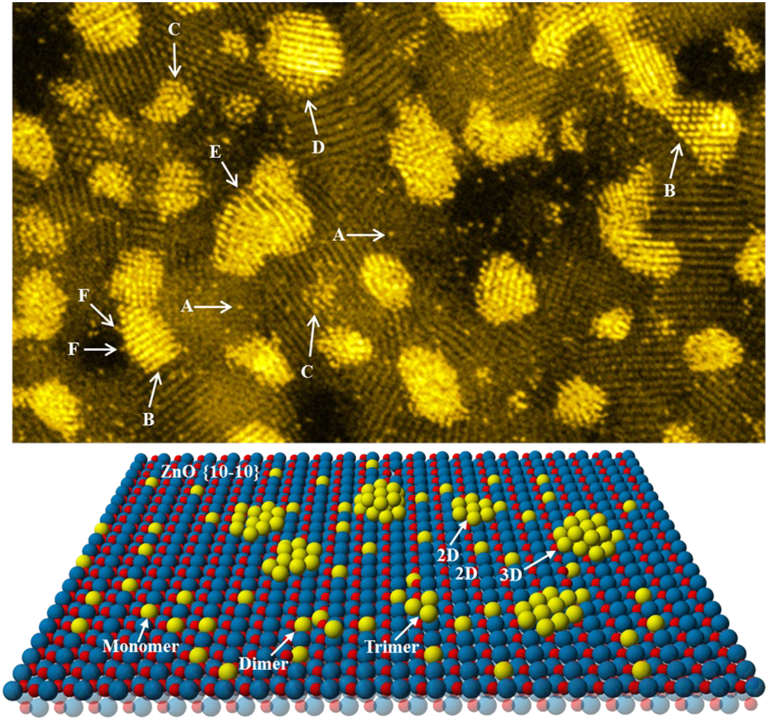
Fig. 9. Top panel: Aberration-corrected HAADF-STEM image of a Pt/ZnO catalyst shows the presence of Pt single atoms (A), faceted Pt clusters (B), highly disordered Pt subnanometer clusters (C), reconstructed surface atoms of Pt nanoparticles (D), strained lattices of Pt (E), and highly unsaturated Pt atoms attached to the Pt nanocrystal (F). Bottom panel: Schematic illustration of the various types of metal clusters, trimers, dimers, and monomers dispersed onto the ZnO {10–10} surface. Reproduced from Liu (Reference Liu2017b).
Bright-Field and Annular Dark-Field STEM Imaging
In addition to his work on understanding the contrast mechanisms of high-resolution TEM images of thin crystals (Cowley & Iijima, Reference Cowley and Iijima1972), Cowley was extremely interested in understanding the contrast of high-resolution STEM images (Cowley, Reference Cowley1973a, Reference Cowley1973b, Reference Cowley1975, Reference Cowley1976; Cowley et al., Reference Cowley, Massover and Jap1974), especially with respect to the nature of dark-field imaging in STEM. Spence & Cowley (Reference Spence and Cowley1978) pointed out that the contrast in STEM lattice images originated from the coherent interference between overlapping CBED discs at the STEM detector position. They also concluded that the intensity at the middle point of the overlapping disks was independent of the beam defocus and aberrations of the probe-forming lens, implying the potential of constructing special detectors for efficient STEM imaging with significantly improved resolution. Enlarging the size of the STEM detector, reduces such interference effects as well as the fringe visibility. Such an understanding of phase-contrast STEM imaging had important consequences on designing special optical systems to be attached to the VG HB5 that ASU installed in 1978 (Cowley & Au, Reference Cowley, Au and Johari1978). With the heavily modified HB5 STEM, Cowley quickly developed shadow-image-based methods for STEM alignment and adjustment (Cowley, Reference Cowley1979a) and explored the readily available imaging modes and microdiffraction from regions as small as the STEM probe size (Cowley & Spence, Reference Cowley and Spence1979). Figure 10 schematically illustrates the detection configuration that Cowley used for his STEM work. With the use of a cold FEG, Cowley observed coherent interference effects within CBED disks and shadow images (Cowley, Reference Cowley1979b).
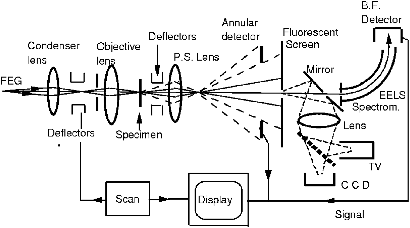
Fig. 10. Diagram of an STEM instrument, modified for the convenient display and recording of shadow images and nanodiffraction patterns. A condenser lens and an objective lens produce the incident electron probe on the specimen and one (or more) post-specimen (P.S.) lenses govern the display of the diffraction pattern on a transmission phosphor screen which may be viewed using a TV-VCR system or a CCD camera with digital recording. The optical lens system can be manipulated by various types of masks. Courtesy of Professor John M. Cowley.
Although Cowley evaluated the ADF STEM imaging mode on his high-resolution HB5 and believed that the wide-angle ADF imaging configuration would provide higher image resolution than the BF STEM imaging mode (Cowley, Reference Cowley1984a, Reference Cowley1984b, Reference Cowley1984c), his research group did not aggressively pursue this direction. Instead, they focused on exploring microdiffraction, in-line holograms, and studies of surfaces (Cowley, Reference Cowley1979b, Reference Cowley1979c, Reference Cowley1979d, Reference Cowley1981a, Reference Cowley1981b, Reference Cowley1982, Reference Cowley1983, Reference Cowley1984a, Reference Cowley1984b, Reference Cowley1984c, Reference Cowley1986; Cowley & Walker, Reference Cowley and Walker1981; Lin & Cowley, Reference Lin and Cowley1986a, Reference Lin and Cowley1986b). By 1984, the present author joined Cowley's research group and started working on Cowley's heavily modified high-resolution VG HB5 (equipped with a special high-resolution pole piece with a spherical aberration coefficient of ~0.8 mm). The optical systems attached to the top of the HB5 column (Fig. 11) facilitated simultaneous observation of an ADF STEM image, energy-filtered image, and a microdiffraction pattern either in the stationary mode or in the scan mode at 10 Mx. Since the optical systems were outside of the electron microscope vacuum chamber, they could be conveniently modified for assessing the effects of various types of STEM detector configurations on the corresponding STEM image contrast. Differences in image contrast were demonstrated by placing either a penny (low-angle ADF) or a quarter (high-angle ADF) coin to block the central portion of the diffraction pattern which could also be contracted or expanded by varying the settings of the two post-specimen lenses. To reduce the effects of light reflection from the metal coin on the ADF image contrast, the present author fabricated a set of disks, from a light-adsorbing black cardboard, of various sizes and shapes as “high-quality” masks to produce a variety of configured STEM images. Since the black cardboard adsorbed light much better than the shiny coins, the atomic number contrast in the ADF STEM images was observably improved. Square and triangular masks were explored. However, the interpretation of images from such exotic STEM detectors became dubious. In retrospect, the lack of high-sensitivity electron detectors, faster computers, image acquisition and processing algorithms, and environmental stability significantly retarded the development of atomic-resolution STEM imaging. The lack of perceived applications of Z-contrast imaging played another important role in not focusing on exploring the capabilities of HAADF imaging mode until projects on characterizing quantum wells (Liu, Reference Liu1990), supported metal catalysts (Liu et al., Reference Liu, Spinnler, Pan and Cowley1990), and mineralogical Franckeite (Pb5Sn3Sb2S14) structures (Wang et al., Reference Wang, Liu, Buseck and Cowley1990, Reference Wang, Buseck and Liu1995) were started.
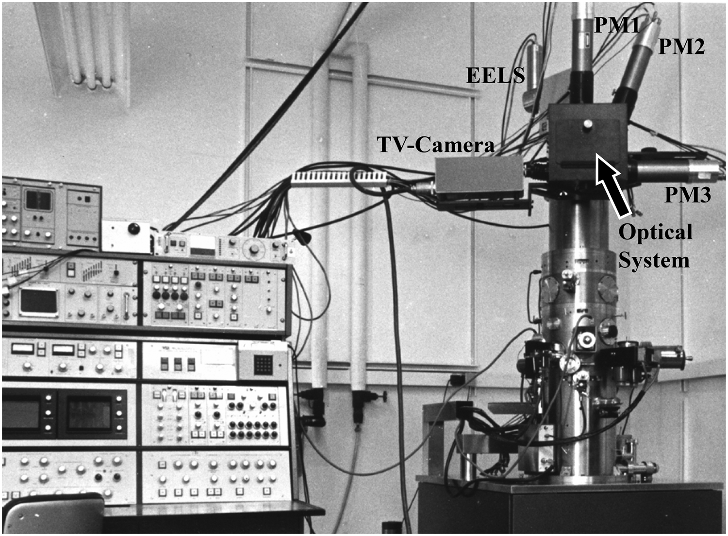
Fig. 11. The heavily modified VG HB-5 STEM of which Professor John M. Cowley used at Arizona State University for all his experimental research work. The black box (indicated by the arrow) contained the unique optical system that transfers the light to various photomultipliers (PM) and the low-light sensitivity TV camera. The annular dark-field images were formed by positioning a light-absorbing mask in the center of the optical lens system. Other types of configured STEM detectors were also tried by masking the various parts of the diffraction pattern displayed on the optical system inside the black box.
The installation of the VG Microscopes HB501UX high-resolution STEM at Oak Ridge National Laboratory in 1988 made it possible for Pennycook and Boatner to obtain chemically sensitive atomic-resolution images of heavy-atom planes in superconductors (YBa2Cu3O7–x and ErBa2Cu3O7–x), directly resolving columns of atoms with different atomic number Z (Pennycook & Boatner, Reference Pennycook and Boatner1988; Pennycook, Reference Pennycook1989a). Their subsequent work on semiconductor interfaces unambiguously demonstrated the atomic number sensitivity of HAADF imaging of crystalline materials and the advantages of this imaging mode over phase-contrast high-resolution TEM (HRTEM) (Pennycook, Reference Pennycook1989b). Unlike phase-contrast HRTEM imaging, the Z-contrast atomic-resolution STEM images did not show obvious contrast reversals with either sample thickness or lens defocus, demonstrating characteristics of incoherent imaging. Previously, multislice simulations of ADF imaging of thin silicon crystal-supported Pt and Au atoms (Kirkland et al., Reference Kirkland, Loane and Silcox1987; Loane et al., Reference Loane, Kirkland and Silcox1988) showed that the image contrast would be oscillatory, probably due to the fact that the inner angle of the ADF detector was not large enough. These image simulations, however, predicted that silicon lattice spacings would be visible and no contrast reversal with increasing sample thickness would be observed, reflecting characteristics of incoherent imaging even when diffracted Bragg peaks were included in the ADF detector. With the use of a slightly larger objective aperture, better image resolution than that of the optimum Scherzer resolution (Scherzer, Reference Scherzer1949) was obtained (Shin et al., Reference Shin, Kirkland and Silcox1989; Xu et al., Reference Xu, Kirkland, Silcox and Keyse1990). It should be realized that the STEM image resolution, especially for ADF imaging, is not well-defined since the STEM probe intensity distribution can be manipulated by varying the size of the probe-forming aperture and the defocus value. If the signal strength is strong enough, sharp-peaked electron probes can provide higher image resolution in ADF/HAADF-STEM images.
To understand the observed characteristics of atomic-resolution HAADF images of crystalline specimens, Pennycook and Jessen conducted Bloch wave analysis, which had been used to understand the thickness-dependent contrast in phase-contrast HRTEM images (Kambe, Reference Kambe1982), of primary electrons propagating through a crystal (Pennycook & Jesson, Reference Pennycook and Jesson1990). The key outcome of this analysis provided a picture that high-angle Rutherford scattering of the incident high-energy electrons was primarily produced by the 1s Bloch state, tightly bound to the atomic nuclei. Therefore, interference effects (among different Bloch states) are significantly reduced. The collected HAADF signal strength was an additive integration through the specimen thickness, increasing monotonically with sample thickness, modulated by small oscillations due to residue interferences among the Bloch states. For very thin samples and under nonchanneling conditions, the HAADF intensity might increase linearly with sample thickness. Because of the highly localized nature of high-angle scattered electrons interference effects, commonly observed in phase-contrast HRTEM images, at interfaces, surfaces, or crystal defects would be minimal or not observable in HAADF-STEM images. Dynamical diffraction and electron-channeling effects would persist for a thicker crystalline specimen, modifying the thickness-dependent trend of the high-angle scattered electrons. The Bloch wave analyses (Pennycook & Jesson, Reference Pennycook and Jesson1990, Reference Pennycook and Jesson1991, Reference Pennycook and Jesson1992) provided an intuitive understanding of the experimentally observed imaging characteristics of atomic-resolution HAADF images of various types of crystalline materials (Chisholm & Pennycook, Reference Chisholm and Pennycook1991; Norton et al., Reference Norton, Lowndes, Pennycook and Budai1991; Pennycook et al., Reference Pennycook and Jesson1991, Reference Pennycook and Jesson1992; Jesson et al., Reference Jesson, Pennycook, Baribeau and Houghton1993a, Reference Jesson, Pennycook, Tischler, Budai, Baribeau and Houghton1993b). It should be pointed out that the degree of interference effects in ADF images strongly depends on the inner collection angle of the annular detector, ranging from complete coherent interference (hole in a disk detector), to partial coherent imaging (annular ring detector), and to completely incoherent imaging (very large inner angle ADF detector or backscattered electron detector).
For STEM imaging, the detector plane contains all the (elastically and inelastically) scattered and nonscattered electrons. At large angles, the electrons scattered by specimen phonons (thermal diffuse scattering) may become dominant (especially for thick specimens, at high temperatures, at surfaces/interfaces, or at various types of defects) while the intensities of Bragg diffraction peaks drop. Phonon-scattered electrons lose a small amount of energy, but the (lateral) momentum transfer can be large, resulting in high-angle scattering events (Hall, Reference Hall1965; Hall & Hirsch, Reference Hall and Hirsch1965; Cowley & Pogany, Reference Cowley and Pogany1968; Earney, Reference Earney1971; Rez et al., Reference Rez, Humphreys and Whelan1977). To evaluate the effects of phonon scattering on the contrast of HAADF images of single crystals and semiconductor interfaces, Wang & Cowley (Reference Wang and Cowley1989, Reference Wang and Cowley1990) incorporated phonon scattering in their multislice calculations. A “frozen-phonon” model (Hall & Hirsch, Reference Hall and Hirsch1965), justified on the basis of the semi-classical argument that incident high-energy electrons “feel” an instant atomic configuration of the crystalline specimen, was introduced into multislice calculations to reproduce key features observed in CBED patterns of a crystalline specimen (Loane et al., Reference Loane, Xu and Silcox1991). Further image simulations with either the frozen-phonon approximation or the Bloch wave approach demonstrated similar results and in agreement with experimental measurements (Loane et al., Reference Loane, Xu and Silcox1992; Hillyard & Silcox, Reference Hillyard and Silcox1993; Hillyard et al., Reference Hillyard, Loane and Silcox1993). These calculations were based on single-phonon scattering processes. Multislice simulations based on a detailed phonon dispersion curve in a crystalline specimen showed that the frozen-phonon approximation was valid for quantitatively understanding the image contrast in ADF images of zone-axis crystals (Muller et al., Reference Muller, Edwards, Kirkland and Silcox2001). However, a system in thermal equilibrium with its environment should not be described by a pure state and a many-body quantum-mechanical model for multiple scattering of fast electrons due to phonon excitations should be used (Forbes et al., Reference Forbes, Martin, Findlay, D'Alfonso and Allen2010). The results of Forbes et al. suggested that treating phonon excitation as one of the inelastic scattering processes would be a more physically meaningful approach. Recent analyses of phonon-scattered electrons supported the model of quantum excitation of phonons and confirmed that the contrast in ADF STEM images would be determined by inelastic scattering events associated with multiple phonon excitations, not consistent with the frozen-phonon model (Hage et al., Reference Hage, Kepaptsoglou, Ramasse and Allen2019).
The resolution of STEM imaging certainly depends on the incident probe size but also on the specific detector configuration. For BF STEM imaging with a small on-axis detector, the image resolution should be similar to that of the corresponding TEM imaging. When the size of the BF STEM detector increases, the image resolution can be improved at the expense of phase contrast. For HAADF-STEM imaging, the incoherent imaging characteristics become dominant. The optimum probe size is determined by the lens properties (e.g., aperture size, aberration coefficients, astigmatism, probe defocus, etc.), the energy of the primary electrons, and the properties of the electron gun. Assuming a coherent point source for a non-aberration-corrected STEM, the optimum defocus value and the optimum aperture size, which defines the optimum semi-convergence angle (α) of the illumination cone at the specimen, are given by Δf = −(λCS)1/2 and α = (4λ/CS)1/4, respectively (Scherzer, Reference Scherzer1949; Crewe, Reference Crewe1983a, Reference Crewe1983b), where CS is the spherical aberration coefficient of the probe-forming lens and λ is the wavelength of the incident electron. For incoherent imaging, the image resolution is defined as δ = 0.43CS 1/4λ 3/4 while for phase-contrast imaging δ = 0.63CS 1/4λ 3/4 (Scherzer, Reference Scherzer1949; Cowley & Iijima, Reference Cowley and Iijima1972). However, since the electron probe intensity distribution plays an important role in determining the observable features in an incoherent HAADF image, it is plausible to manipulate the probe intensity distribution to gain better image resolution at the expense of image contrast (Liu, Reference Liu1990; Liu & Cowley, Reference Liu and Cowley1993). Loane et al. (Reference Loane, Xu and Silcox1992) predicted that by defocusing the electron beam, it would be possible to achieve an image resolution beyond the Scherzer-focus resolution limit of an uncorrected STEM instrument. Such a practice becomes less relevant with aberration-corrected STEM instruments. By using configured STEM detectors, the STEM image resolution can be further improved (Cowley, Reference Cowley1993) provided that one can correctly interpret the image contrast. The effectiveness of such strategies on extracting useful information about the specimen needs to be re-evaluated on aberration-corrected STEMs.
With continuous improvement in image resolution, especially after lens aberrations were corrected, the measurement of image resolution became a nontrivial problem (O'Keefe, Reference O'Keefe1992; O'Keefe & Allard, Reference O'Keefe and Allard2004; O'Keefe et al., Reference O'Keefe, Allard and Blom2005; Smith, Reference Smith2008). Furthermore, how to define the resolution in a microscope image needs to be carefully evaluated as well (Rayleigh, Reference Rayleigh1879; Sparrow, Reference Sparrow1916; Black & Linfoot, Reference Black and Linfoot1957). Depending on the nature of aberration-corrections of the microscope, the evaluation of conditions for obtaining an optimum STEM probe size required careful consideration (Kirkland, Reference Kirkland2011; Sasaki et al., Reference Sasaki, Sawada, Okunishi, Hosokawa, Kaneyama, Kondo, Kimoto and Suenaga2012). The optical transfer function of the probe-forming lens, relevant for understanding information transfer of the specific lens system, should be studied in three dimensions (Fig. 12; Jones & Nellist, Reference Jones and Nellist2014). For practical measurement of image resolution, not only the lens parameters are important but also the nature of the specimen, the intrinsic properties of the scattered electrons, and the type of the STEM detector that is used to obtain the image all become relevant (Peng et al., Reference Peng, Oxley, Lupini, Chisholm and Pennycook2008). The ultimate information transfer limit in an HAADF-STEM image is controlled by the effective size of the objective aperture provided that external interferences, instabilities, and the signal-to-noise ratio are not the limiting factors. Even for the smallest probe size, which is available on the newest generation ac-STEMs, accurate measurement of the “sizes” of various types of individual atoms needs to be carefully scrutinized and verified since the recorded “sizes” of the bright-dots in HAADF-STEM images originate from the convolution of the probe intensity distribution with the effective “atom sizes” which may depend on detector configuration, robustness of the specimen under electron irradiation, and environmental factors.
Fig. 12. Left-hand panel: the 3D optical transfer versus defocus iso-surface for a simulated probe with a “real” mixture or aberration strengths, orientations, and other microscope properties. Bounding surface shows 10% optical level. Right-hand panel: sections through the modulus of the 3D optical transfer function in the reciprocal x-direction (left half) and at 90° from this, in the reciprocal y-direction (right half). Reproduced from Jones & Nellist (Reference Jones and Nellist2014).
Configured Detectors for Versatile STEM Imaging
STEM provides various approaches to extracting information from the specimen of interest. The variable sizes and configurations (via adjustment of post-specimen lenses, use of masks, or digital manipulation) of BF and/or ADF detectors can be employed to form images. Such a flexibility, however, poses a critical question on the interpretability of the acquired STEM images. Each type of signal, generated from the interaction of a coherent electron probe with a specimen, can be collected to form the corresponding image which carries specific information about the specimen. Historically, a critical question arises on the nature of the acquired STEM image: coherent versus incoherent formation of images. Such a distinction is critical to understanding the interpretability of, and the ultimate achievable image resolution in, the acquired STEM image. The secondary (emitted) signals such as X-rays, secondary electrons, Auger electrons, or cathodoluminescence light quanta are considered to be incoherent, although the effects of incident electron channeling in crystalline specimens still play a role in determining the collected signal strength. For high-energy primary electrons transmitted through a thin crystal, however, the situation can become complicated. First, with the use of a cold FEG and an optimum probe-forming aperture, all electrons within a small electron probe can be considered fully coherent. The reciprocity principle suggests that, with the use of a small (ideally a delta function) STEM detector, the acquired STEM image can be fully interpreted as a BF/DF phase-contrast TEM image. This statement is valid regardless of the probe size as long as it is fully coherent. Spence & Cowley (Reference Spence and Cowley1978) pointed out that unless the small STEM detector was positioned at the overlapping regions of the diffraction disks lattice fringes (due to interference effect) of a crystalline specimen would not be obtained. Such a requirement for overlapping diffraction disks demands an effective minimum convergence angle of the incident probe or the size of the probe-forming aperture, which determines the minimum probe size if the lens aberrations are fully corrected. Lattice fringes with spacings smaller than the probe size can be observed as long as the STEM probe is fully coherent and the diffraction disks overlap (Liu & Cowley, Reference Liu and Cowley1991, Reference Liu and Cowley1993). In order to understand the image contrast and resolution of STEM images obtained with configured STEM detectors, we provide here a simple qualitative description of STEM imaging (Cowley, Reference Cowley1993; Liu & Cowley, Reference Liu and Cowley1993) and relate the critical role of the size and shape of the STEM detectors to the contrast of the corresponding STEM images.
When a small, coherent electron probe interacts with a crystalline specimen in an STEM instrument, the incident electrons are scattered both elastically and inelastically. If the specimen is thin enough, then all the incident electrons can penetrate through the specimen (conservation of the total electron flux). Such an assumption is generally valid for atomic-resolution STEM imaging. At the exit surface of the specimen, the amplitude distribution of electrons scattered into a solid angle Ω with an energy E can be described by a wave function ψ(Ω, E), where E is the energy of the (elastically or inelastically) scattered electrons. For elastic scattering, E = E 0 (incident electron energy). For inelastic scattering, E = E 0 − ΔE, where ΔE is the energy loss of the incident electrons due to inelastic scattering events by sample electrons or phonons. At the far-field (Fraunhofer diffraction condition) detector plane, a diffraction pattern appears and can be recorded by a camera. Ideally, the diffraction pattern should be separated into many individual sets of patterns by a spectroscopic-diffraction approach: Each diffraction pattern is recorded with a specific electron energy. For example, elastically scattered electrons provide a zero-energy-loss diffraction pattern while the diffraction pattern obtained with a phonon energy loss reflects the momentum distribution of the incident electrons which are inelastically scattered by the specific type of specimen phonon excitation. Quantitative analysis of such spectroscopic-diffraction data should provide all useful information about the various electron–specimen interaction processes and consequently the nature of the specimen of interest.
If only electrons scattered along the direction K are considered, then the wave function, emerging at position X on the exit surface of the specimen, can be represented as ψ(K, X, E), where K is a two-dimensional reciprocal space vector with the amplitude determined by  $\vert {\boldsymbol K}\vert = 2\sin \left({{\theta \over 2}} \right)/\lambda$ (θ is the scattering angle and λ is the wavelength of the scattered electron with energy E) and X is a two-dimensional vector in real space, describing the coordinate of the electron probe at the exit surface of the specimen. When the electron probe is scanned across a specimen, the variations in the five-dimensional wave function ψ(K, X, E) carry all the relevant information about the specimen structure and chemistry. Since the wave function ψ(K, X, E) is not an observable, what is experimentally recorded at the STEM detector plane is the intensity I(K, X, E), which is proportional to |ψ(K, X, E)|2. Assuming that the elastically scattered electrons do not coherently interfere with the inelastically scattered electrons, then the experimentally (without energy filtering) recorded intensity is $I( {{\boldsymbol K}, \;{\boldsymbol X}} ) = \int {I( {{\boldsymbol K}, \;{\rm \;}{\boldsymbol X}, \;{\rm \;}E} ) dE}$. It should be noted that when the electron probe is moved across a specimen, the local intensity of the diffraction pattern may redistribute, but the integrated total intensity of the whole diffraction pattern should be constant regardless of the probe position and probe size (preservation of the electron flux). The integration over energy may impose strict requirements on sample thickness and incident beam energy: Extremely thin samples or use of very high incident electron energies simplify the image interpretation.
When the detected signal, corresponding to each probe position, is displayed, a two-dimensional image is formed. Variations in the signal strength, collected by the STEM detector, provide image contrast. The various types of STEM images include X-ray maps, secondary electron images, Auger electron images, images formed with elastically scattered electrons or inelastically scattered electrons, etc. In the following discussion, we only focus on STEM images that are formed by collecting elastically or inelastically scattered primary electrons. For each fixed probe position X, a full diffraction pattern appears on the detector plane. If each detector pixel records and converts the detected signal independently, then the detected signal strength corresponding to the specimen position X can be expressed as
 $$I( {\boldsymbol X} )\! =\! \int {D( {\boldsymbol K} ) {\vert {\psi ( {{\boldsymbol K}, \;{\boldsymbol X}} ) } \vert }^2d{\boldsymbol K \!=\! }\iint \! {D( {K_x, \;K_y} ) {\vert {\psi ( {K_x, \;K_y, \;{\boldsymbol X}} ) } \vert }^2dK_xdK_y} }, $$
where D(K) is a two-dimensional detector function (The detector function is usually a step function but can become more complicated to represent a configured detector). We dropped the energy dependence of the wave function on the assumption that the STEM detector collects all the elastically and inelastically scattered electrons with equal efficiency. For a thin specimen, all the transmitted electrons arrive at the detector plane and the detector response can be assumed to be independent of angle and energy of the scattered electrons (This assumption is correct for general ADF and BF detectors. However, this assumption is not correct when an electron spectrometer is used). Under these assumptions, the intensity integration over the whole two-dimensional detector plane should be constant (preservation of the incident electron flux). By adding the signal strength of all the STEM detectors that cover the whole diffraction plane, we obtain
 $$I( {\boldsymbol X} ) = \sum\limits_i {\int_{K_i}^{K_{i + 1}} {D_i( {\boldsymbol K} ) {\vert {\psi ( {{\boldsymbol K}, \;{\boldsymbol \;X}} ) } \vert }^2d{\boldsymbol K}\equiv {\rm C}} }, $$
where Di(K) represents the detector function of the ith STEM detector, the summation is over all the STEM detectors, and C is a constant. In equation (2), the total probe intensity can be normalized to unity (C = 1). The physical picture of equation (2) can be visualized as if the whole diffraction pattern at the detector plane is filled with independent STEM detectors of various sizes and shapes. The summation of the intensities of all the STEM detectors represents the total intensity of the whole diffraction pattern, which should be constant and does not depend on the probe position, probe size, defocus, or lens aberrations. Equation (2) clearly demonstrates the flexibility of STEM detectors and the intrinsic relationship among these detectors. Even though an infinitely large STEM detector, which can be divided into many detectors of various shapes and sizes, does not provide any information about the specimen, each individual detector, regardless of its size and shape, provides specific information about the specimen. The size, shape, and position of each individual STEM detector control the image contrast and the resolution of the corresponding STEM image if the incident probe size is small enough.
If a point STEM detector, which is represented by δ (K-G) (where G is a vector drawn from the optic axis to any point on the diffraction pattern), is used, then equation (1) gives I(X) = |ψ(G, X)|2. When G is at the optic axis or at a Bragg diffraction spot of a crystalline specimen, the STEM image is equivalent to a BF or tilted DF TEM image with parallel illumination, respectively. If the STEM detector is slightly enlarged but is still considered to be small, then the STEM image is equivalent to the corresponding TEM image obtained with an incoherent convergent illumination, blurring the phase-contrast features. When the CBED disks overlap, lattice fringes should be detected if the small STEM detector is positioned within the overlapping regions. Two-dimensional fringes should be formed when the STEM detector is positioned at any point within the regions that three or more noncollinear diffraction disks overlap. Therefore, atomic-resolution phase-contrast BF and DF STEM images can be obtained and interpreted, similar to those of HRTEM images. Such imaging modes, however, do not have any advantages over the HRTEM technique, except for nanoanalysis and nanodiffraction studies, or for imaging thicker samples.
If many small STEM detectors  $( D( {\boldsymbol K}) = \sum\nolimits_0^N {\delta ( {\boldsymbol K}-{\boldsymbol G}_n) ) }$ are used together to collect all the Bragg diffracted peaks and the transmitted beam (or if all the diffracted and transmitted spots are excluded), then the image contrast in the corresponding STEM image should highlight specimen features that cause diffuse scattering (phonon scattering plus diffuse scattering from defects). If the diffraction disks overlap, one can collect all the equivalent overlapping regions to enhance the signal-to-noise and signal-to-background ratios. In the late 1980s, the present author tried these approaches on Cowley's unique optical systems attached to his high-resolution VG HB5. Due to the low signal-to-noise ratio and complications in precisely positioning the masks at the desired locations, such work, however, did not yield fruitful results. Nowadays, such a scheme can be easily accomplished by using high-quality electron detectors, digital acquisition and processing methods, and reconstruction algorithms, leading to four-dimensional electron microscopy which will be discussed later.
If only two complementary STEM detectors are used to collect the whole electron diffraction pattern, then the corresponding STEM images are complementary to each other regardless of the shape, size, or position of the two detectors. A simple example consists of a disk detector and a complementary annular detector, both centered at the optic axis, covering the whole electron diffraction pattern at the detector plane. The relationship between the two complementary STEM images is given by
 $$I( {\boldsymbol X} ) = \int_{u_C}^\infty {D( u ) {\vert {\psi ( {u, \;{\boldsymbol X}} ) } \vert }^2du = 1-\int_0^{u_C} {D( u ) {\vert {\psi ( {u, \;{\boldsymbol X}} ) } \vert }^2du} }, $$
where uC represents the radius of the disk detector or the inner radius of the annular detector. For a thin specimen, the signal strength of electrons, which are scattered to very large angles, is negligible. In this case, extending the integration over the outer radius of the annular detector to infinity should not introduce appreciable error. For thick specimens, which most probably is not relevant to high-resolution imaging, such an approximation is not valid (Liu & Cowley, Reference Liu and Cowley1991, Reference Liu and Cowley1993). In theory, subtraction of a uniform background from an STEM image should not modify the characteristics of the corresponding image. Therefore, the normalized image contrast of the two complementary STEM images can be considered as C ADF(X) = −CBF(X). Regardless of the size of the inner angle of the annular detector, the corresponding BF STEM image (right-hand side of (3)) is always complementary to the ADF STEM image (left-hand side of (3)) and these pair images should always possess the same imaging characteristics. By generalizing this specific example, one can state that the two complementary STEM images should contain the same amount of information but with a contrast reversal. From this perspective, an HAADF-STEM image, regardless of the inner collection angle, contains the same type of information about the specimen as the corresponding complementary BF (cBF) STEM image does.
When uC becomes small (small inner collection angle of the ADF detector), phase contrast may become dominant in the low-angle ADF STEM image. When uC becomes large, the phase contrast is suppressed and the Z-contrast can become dominant in both the HAADF and the cBF pair images, complementary to each other, and the image resolution can be significantly improved in both images (Liu, Reference Liu1990; Liu & Cowley, Reference Liu and Cowley1991, Reference Liu and Cowley1993). The contrast in an STEM image strongly depends on the specific size, shape, and position of the STEM detector, varying from predominantly interference-based phase contrast to incoherent Z-contrast. In fact, any types of STEM detector can be designed and implemented to acquire useful information about the specimen. Cowley explored different types of STEM imaging modes by developing specialized detectors (Cowley, Reference Cowley1993; Cowley & Liu, Reference Cowley and Liu1993; Cowley et al., Reference Cowley, Hansen and Wang1995). In particular, he focused on the use of a thin annular detector (TAD) to select the specific angular range of the scattered electrons for resolution improvement and/or for contrast enhancement of specific elements of interest. By employing a TAD (with a width equal to ~10% of the inner radius) and the use of post-specimen lenses, Cowley developed several STEM imaging modes including the TAD-based BF, DF, and marginal imaging configurations (Cowley, Reference Cowley1993, Reference Cowley2001; Cowley et al., Reference Cowley, Hansen and Wang1995; Liu & Cowley, Reference Liu and Cowley1996). He discussed why these special imaging modes, based on the estimation of the point spread functions, would provide much better image resolution. By selecting the appropriate angular range with a TAD, light-element clusters dispersed on heavy-element supports can be distinguished (Liu & Cowley, Reference Liu and Cowley1996; Cowley, Reference Cowley2001). For the STEM marginal imaging mode, the image contrast is proportional to the square of the differential of the projected specimen potential, and thus any deflection of the incident beam spot due to a change of the projected potential gives bright contrast in the marginal TAD STEM images.
The angular dependence of scattered electrons, combined with the intrinsic characteristics of annular ring detectors, was used for special purposes (Cowley, Reference Cowley2001). Such an angular-filtered imaging strategy was used to image thick amorphous/biological samples and other types of materials (Smith & Cowley, Reference Smith and Cowley1975; Liu & Cowley, Reference Liu and Cowley1991, Reference Liu and Cowley1993, Reference Liu and Cowley1996; Haider et al., Reference Haider, Epstein, Jarron and Boulin1994; Cowley, Reference Cowley2001; Hyun et al., Reference Hyun, Ercius and Muller2008; de Jonge et al., Reference de Jonge, Peckys, Kremers and Piston2009; Zhang et al., Reference Zhang, Hwang, Isaac and Stemmer2015). The flexibility of designing and developing STEM detectors affords us to explore the reciprocal space of the specimen in many different ways. By selecting specific regions of the reciprocal space, one can extract specific type of information that is present in the real space. For example, angle-selective (or momentum-selective) imaging approaches have been effectively utilized (Daberkow et al., Reference Daberkow, Herrmann and Lenz1993; Haider et al., Reference Haider, Epstein, Jarron and Boulin1994; Hammel & Rose, Reference Hammel and Rose1995; Zhang et al., Reference Zhang, Hwang, Isaac and Stemmer2015; Müller-Caspary et al., Reference Müller-Caspary, Oppermann, Grieb, Krause, Rosenauer, Schowalter, Mehrtens, Beyer, Volz and Potapov2016; Johnson et al., Reference Johnson, Im, Windl and Hwang2017). By selecting a small range of low scattering angles, the contrast of defect-containing atomic columns was investigated (Johnson et al., Reference Johnson, Im, Windl and Hwang2017). Although the image contrast is still affected by the sample thickness, crystal orientation, local strain, and probe convergence angle, the angle-selective imaging method opens new possibilities for 3D structural characterization of individual point defects in functional materials.
Annular Bright-Field (ABF) and Differential Phase-Contrast STEM Imaging
Based on the reciprocity principle, phase-contrast STEM images should be obtainable by placing a small axial detector at the optical axis of the microscope. BF STEM images acquired with such small disk detectors, however, usually have very low signal-to-noise ratio since the majority of the transmitted/scattered electrons within the illumination cone are excluded. The signal-to-noise issue becomes more problematic for atomic-resolution STEM imaging with small-probe sizes which require large probe-forming apertures. Thomson analyzed the image quality issues and proposed to use large-axial BF STEM detectors to enhance signal strength without compromising too much on phase contrast (Thomson, Reference Thomson1973). Similar to phase-contrast TEM images, phase-contrast STEM images of a periodic crystal lattice have no obvious plane of focus for maximum interpretability since the electron waves, originated from different atomic sites, constructively or destructively interfere at different image planes (Cowley & Moodie, Reference Cowley and Moodie1957). At each focal plane, the relationship between the positions of the “atom” columns in the image and the actual positions of atom columns in the crystal unit cell is typically ambiguous; rigorous image simulations are usually required to extract the exact positions of atomic columns. The flexibility of configuring the STEM detector provides a unique approach to forming different types of images that contain specific types of specimen information. After carefully examining the potential imaging modes on an STEM, Rose explored the use of an annular bright-field (ABF) detector to improve the quality of phase-contrast STEM images (Rose, Reference Rose1974; Fertig & Rose, Reference Fertig and Rose1979). Rose proposed simultaneous acquisition of two types of images: One detector system consisted of an ABF detector to collect BF signal from the outside of the illumination cone and another BF disk detector beneath the ABF detector to collect the remaining BF signal. Rose further proposed that the image contrast would be enhanced by taking the difference between the simultaneously registered signals from the two detectors. Such STEM images might result in improved resolution over that of the CTEM or BF STEM images.
Based on the reciprocity principle, TEM images obtained with hollow-cone illumination (Mathews, Reference Mathews1953) or the use of a ring-shaped condenser aperture should provide similar high-resolution images obtained with an ABF or TAD detector. Therefore, the contrast transfer in ABF imaging is expected to yield better image resolution than the conventional BF STEM and possesses nonoscillating contrast transfer characteristics (Saxton et al., Reference Saxton, Jenkins, Freeman and Smith1978). Early experimental results demonstrated the advantages of such a TEM imaging mode, revealing simultaneously different sets of lattice fringes of Au nanoparticles (Heinemann & Poppa, Reference Heinemann and Poppa1970) and DF/BF imaging with the hollow-cone illumination resolved isolated heavy atoms (Thon & Willasch, Reference Thon and Willasch1972). The ring-shaped objective aperture in TEM was tried to enhance image resolution and contrast in DF TEM images (Heinemann & Poppa, Reference Heinemann and Poppa1972). The use of ring-shaped condenser apertures or hollow-cone illumination was expected to yield images free of chromatic aberration effects (Komoda, Reference Komoda1966; Cowley, Reference Cowley1973a), and significant improvement in image resolution as well as the signal-to-noise ratio were obtained (Mathews, Reference Mathews1953; Cowley, Reference Cowley1973a, Reference Cowley1973b; Rose, Reference Rose1977; Dinges et al., Reference Dinges, Kohl and Rose1994; Rosenauer et al., Reference Rosenauer, Krause, Müller, Schowalter and Mehrtens2014).
Although Cowley investigated the potential advantages of the various types of TAD detectors including the TAD-based BF configurations (Cowley et al., Reference Cowley, Hansen and Wang1995; Cowley, Reference Cowley2001), the full advantages of atomic-resolution ABF imaging of light elements in practical crystalline samples were not clearly demonstrated until much later. Okunishi et al. (Reference Okunishi, Ishikawa, Sawada, Hosokawa, Hori and Kondo2009), using an aberration-corrected TEM/STEM which was equipped with an ABF and an ADF detector to simultaneously acquire both ABF and HAADF images, unambiguously and clearly resolved both cations and anions in SrTiO3 and Fe3O4 samples. In a subsequent paper, Findlay et al. (Reference Findlay, Shibata, Sawada, Okunishi, Kondo, Yamamoto and Ikuhara2009) discussed the image contrast variations with sample thickness and electron probe defocus. Based on the s-state channeling model of fast electrons (Van Dyck & Op de Beeck, Reference Van Dyck and Op de Beeck1996), Findlay et al. (Reference Findlay, Shibata, Sawada, Okunishi, Kondo, Yamamoto and Ikuhara2009) generalized such an electron propagation model to explain the experimentally observed ABF image contrast. Through both experimental results and systematic simulations, the authors demonstrated that an ABF detector would produce an “absorption” image, revealing both heavy- and light-atom columns of a zone-axis crystal. The authors further demonstrated that ABF images, complementary to simultaneously acquired HAADF images, were robust and interpretable over a wide range of specimen thicknesses. The characteristics of the ABF imaging mode are very different from those of pure phase-contrast TEM/STEM imaging modes, and the ABF method constitutes a powerful approach to identifying atom locations of both light and heavy elements in a crystalline specimen.
Findlay et al. (Reference Findlay, Saito, Shibata, Sato, Matsuda, Asano, Akiba, Hirayama and Ikuhara2010a, Reference Findlay, Shibata, Sawada, Okunishi, Kondo and Ikuhara2010b) further investigated the dynamics of ABF image formation and its contrast characteristics. These studies firmly established the foundations of reliably imaging both light- and heavy-element columns over a range of sample thicknesses. The authors discussed the dependence of ABF image contrast on specimen thickness, detector configuration, probe size/defocus, and the sensitivity of this imaging method to intercolumn spacing and local crystal disorder. Through a comprehensive image simulation study, the authors confirmed the robustness of the ABF imaging mode with respect to sample thickness and a limited defocus range over which the ABF images would be directly interpretable. They further demonstrated that, unlike the HAADF imaging mode, the ABF image contrast might not have an intuitively interpretable dependence on the atomic number of the element of interest. The s-state electron-channeling model is intuitively simple but has its limitations. For example, such a simplified model breaks down when the intercolumn spacing becomes small enough that the s-states of adjacent columns of atoms overlap (Anstis et al., Reference Anstis, Cai and Cockayne2003). Both experimental studies and image simulations (Findlay et al., Reference Findlay, Saito, Shibata, Sato, Matsuda, Asano, Akiba, Hirayama and Ikuhara2010a, Reference Findlay, Shibata, Sawada, Okunishi, Kondo and Ikuhara2010b) showed that the ABF image intensity of atomic columns oscillated with sample thickness, especially for thin specimen and/or light elements. Although the s-state electron-channeling model is adequate for interpreting ABF image contrast of certain light elements, thermal diffuse scattering should be considered for understanding the ABF image contrast of heavy elements. Diffuse scattering of incident electrons may play a more important role in ABF images obtained with smaller probe sizes (larger illumination cone), of crystals containing defects/disorders, or of thicker specimens.
The simple s-state channeling model may not work well for understanding ABF images of ultra-light elements, such as hydrogen or lithium, since the attractive potential to confine the electrons traveling along the atomic columns is relatively weak. The optimization of the ABF imaging detector configurations was conducted. For example, Ohtsuka et al. (Reference Ohtsuka, Yamazaki, Kotaka, Hashimoto and Watanabe2012) studied the image characteristics of a middle-angle BF (MABF, complementary to ABF) and concluded that both light O atomic columns and heavy Sr and Ti–O atomic columns of SrTiO3(001) were visible with distinct bright and dark contrast over practical ranges of the probe-forming lens defocus and sample thickness. The authors claimed that the difference in contrast between heavy and light atomic columns is greater than that of ABF STEM images. Furthermore, Findlay et al. (Reference Findlay, Kohno, Cardamone, Ikuhara and Shibata2014) developed an enhanced-ABF (eABF) imaging mode to achieve a higher image contrast for light-element columns by subtracting the images obtained from these two complementary MABF and ABF detectors. These improvements are based on configuring detector size/geometry and signal manipulations, representing specific examples of the STEM configured detectors discussed in the section “Configured detectors for versatile STEM imaging”. A recent example of such development is the use of annular segmented-detector configuration to enhance the image contrast of light elements by mathematical manipulation of different types of STEM images (Ooe et al., Reference Ooe, Seki, Ikuhara and Shibata2019).
The most important characteristics of ABF imaging is the precise and simultaneous identification of atom positions of both light- and heavy-element columns in a zone-axis crystal. The HAADF image intensity strongly depends on the atomic number (~Z 4/3-2) and the inner collection angle (Treacy, Reference Treacy2011). Although it is difficult to establish a direct relationship between the ABF signal strength and the atomic number of the probed element, Findlay et al. (Reference Findlay, Saito, Shibata, Sato, Matsuda, Asano, Akiba, Hirayama and Ikuhara2010a, Reference Findlay, Shibata, Sawada, Okunishi, Kondo and Ikuhara2010b) proposed, under relatively ideal imaging and specimen conditions, a weaker dependence of ABF signal strength on the atomic number (~Z 1/3). The significantly reduced dependence on atomic number Z makes it possible to visualize both light and heavy elements in the same ABF image. To appreciate the effect of such difference in the Z-dependence on atom visibility in ABF and HAADF images, Figure 13 shows the plots of Z 1.7 (representing HAADF imaging) and Z 0.33 (representing ABF imaging) versus atomic number Z. Although such a comparison is not necessarily rigorous, one can immediately and intuitively understand that compared with the HAADF signal strength, the ABF signal strength only weakly depends on the atomic number Z, leading to appreciable atom visibility for all elements within a specimen. On the other hand, the large difference in signal strength between a light element (e.g., Li) and a relatively heavy element (e.g., Co) in an HAADF image overshadows the visibility of the light element due to the integrated effects of (1) nonlocal nature of the probe intensity profile, (2) nonlocalized scattering cross-sections, and (3) short distances among the nearest atom columns of different elements within a crystal. Figure 13 implies that the chemical sensitivity of the HAADF imaging mode is much higher than that of the ABF imaging mode. Without detailed image simulations, one may not be able to intuitively correlate the absorption contrast in ABF images with the atomic number Z of the elements of interest. Under certain imaging conditions, contrast reversal in ABF images can occur. For example, Lee et al. (Reference Lee, Oshima, Hosono, Zhou and Takayanagi2013) reported that for very thin specimens, ABF images showed dark dips at atomic columns in over-focus and reversed to bright peaks in under-focus. These authors further demonstrated that for the same incident probe convergence angle, the depth of focus (DOF) was narrower in an ABF image than in an HAADF image and the optimum defocus for ABF imaging was closer to the specimen surface. The combination of the ABF imaging mode with the corresponding HAADF imaging mode, however, significantly enhances the power of STEM in solving challenging materials problems. ABF STEM imaging, in combination with HAADF imaging, provides quantitative measurement of local structure distortion, especially for structural investigations of complex oxides (Aso et al., Reference Aso, Kan, Shimakawa and Kurata2013, Reference Aso, Kan, Shimakawa and Kurata2014; Gao et al., Reference Gao, Kumamoto, Ishikawa, Lugg, Shibata and Ikuhara2016a; Kim et al., Reference Kim, Pennycook and Borisevich2017).
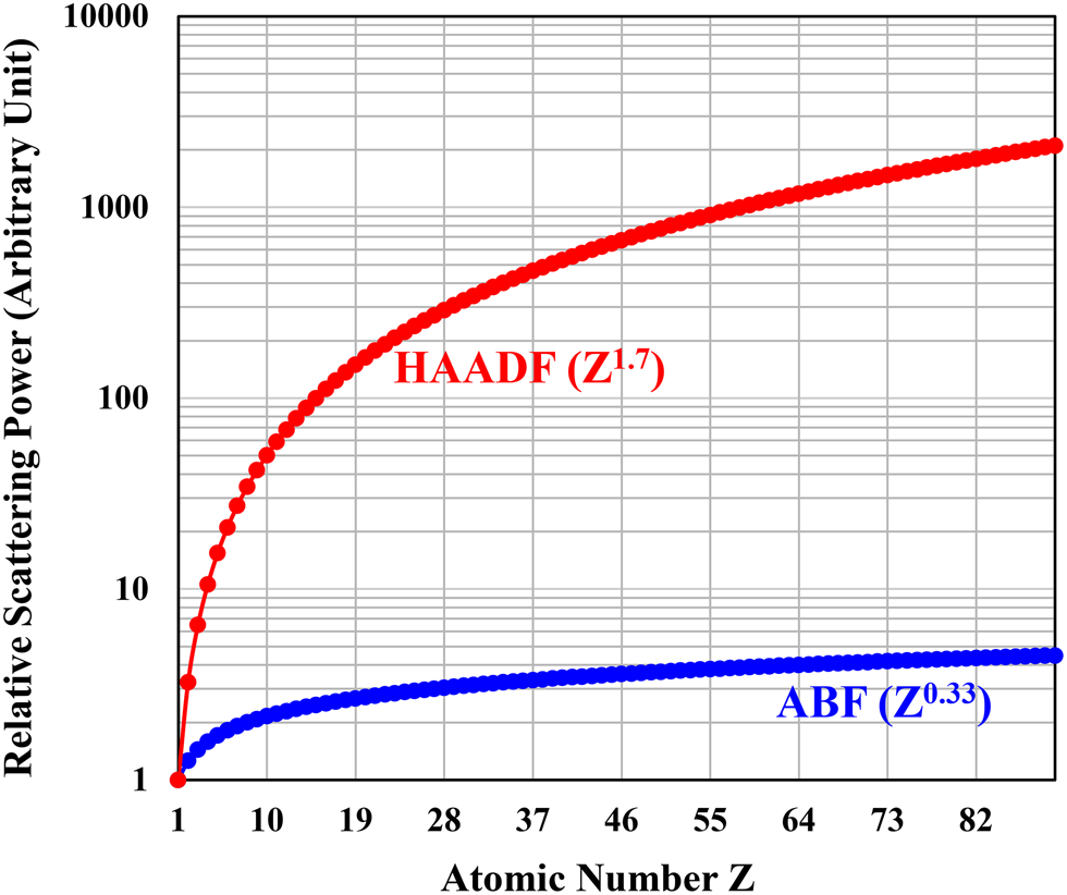
Fig. 13. Plots of the dependence of HAADF (~Z 1.7) and ABF (~Z 1/3) signal strength on the atomic number Z.
Full understanding of the factors that affect the precise measurement of atom positions in ABF images is of importance for precise measurement of distances and angles between different atomic columns in a crystal. Based on the dynamical scattering theory, Van Dyck et al. (Reference Van Dyck, Bokel and Zandbergen1998) discussed the effects of different range of specimen tilt on electron channeling in crystalline specimens. Investigations on how a specimen tilt affects the contrast of atomic-resolution ADF STEM images were conducted (Yamazaki et al., Reference Yamazaki, Kawasaki, Watanabe, Hashimoto and Shiojiri2002; Maccagnano-Zacher et al., Reference Maccagnano-Zacher, Mkhoyan, Kirkland and Silcox2008; Yu et al., Reference Yu, Muller and Silcox2008; So & Kimoto, Reference So and Kimoto2012; Cui et al., Reference Cui, Yao, Wang, Shen and Yu2017). Since the contrast of an ABF image is at least partially determined by the phase of the forward-scattering electrons, the tilt of the incident electron beam with respect to a crystal zone axis may have a larger impact on ABF imaging than on HAADF imaging. Specimen tilt might cause significant artifact in extracting correct atom positions from STEM images. For example, Gao et al. (Reference Gao, Liu, Huang, Chu, Ishikawa, Feng, Jiang, Shibata, Wang and Ikuhara2016b) found that in a tilted crystal, the shift of atom positions depended on atom species, that is, larger shift for lighter anion columns and smaller shift for heavier cation columns. They also found that the tilt-induced displacement of atom positions depended on electron probe defocus, incident beam convergence angle, and specimen thickness. Zhou et al. (Reference Zhou, Mueller-Caspary, Sigle, Krause, Rosenauer and van Aken2016) investigated the deviations of atom positions in ABF images from those of the corresponding ADF images and studied the effect of specimen tilt on the bond angle measurements in ZrO2. Brown et al. (Reference Brown, Ishikawa, Sanchez-Santolino, Lugg, Ikuhara, Allen and Shibata2017) proposed a method for evaluating and correcting specimen tilt by simultaneously recording a central BF STEM and the corresponding ABF STEM image. Kim et al. (Reference Kim, Pennycook and Borisevich2017) quantitively compared the BF and ABF STEM images and discussed the robustness of structural measurements of oxygen octahedral tilts as a function of specimen tilt and electron probe defocus. With the understanding of the characteristics of the ABF imaging mode, picometer-scale atom position determination of light elements became plausible (Gao et al., Reference Gao2018).
The simultaneous acquisition of HAADF and ABF images to visualize atomic columns of a large range of various cations and anions is critical to atomic-scale study of materials systems that consist of both light and heavy elements. The development of the ABF imaging mode significantly enhanced the power of atomic-resolution STEM imaging of a wide variety of crystalline specimens. Such atomic-resolution imaging capabilities proved to be essential for correlating macroscopic properties of complex oxides to the small changes of ligand coordination or the exact arrangement of oxygen sub-lattice at hetero-interfaces (Huang et al., Reference Huang, Ding, Liang, Gao, Tang, He, Duan, Zhu, Chu, Fisher, Hirayama, Ikuhara and Chu2014). Because of its power in resolving atomic columns of light elements, the ABF imaging method was readily applied for direct imaging of hydrogen columns in crystalline solids (Findlay et al., Reference Findlay, Saito, Shibata, Sato, Matsuda, Asano, Akiba, Hirayama and Ikuhara2010a, Reference Findlay, Shibata, Sawada, Okunishi, Kondo and Ikuhara2010b; Ishikawa et al., Reference Ishikawa, Okunishi, Sawada, Kondo, Hosokawa and Abe2011; Kim et al., Reference Kim, Tao, Klie and Seidman2013), Li atoms in battery-related materials (Oshima et al., Reference Oshima, Sawada, Hosokawa, Okunishi, Kaneyama, Kondo, Niitaka, Takagi, Tanishiro and Takayanagi2010; Gu et al., Reference Gu, Zhu, Li, Yu, Li, Tsukimoto, Maier and Ikuhara2011, Reference Gu, Xiao, Hu, Li and Ikuhara2015; Huang et al., Reference Huang, Hitosugi, Findlay, Fisher, Ikuhara, Moriwake, Oki and Ikuhara2011; Lee et al., Reference Lee, Oshima, Niitaka, Takagi, Tanishiro and Takayanagi2012; Yu et al., Reference Yu, Ishikawa, So, Shibata, Kudo, Zhou and Ikuhara2013; Findlay et al., Reference Findlay, Huang, Ishikawa, Shibata and Ikuhara2017), and a plethora of other materials systems. Other example applications of ABF STEM imaging include visualization of oxygen vacancies in a perovskite oxide (Kobayashi et al., Reference Kobayashi, Findlay, Shibata, Mizoguchi, Sato, Okunishi, Ikuhara and Yamamoto2012), observation of electrically induced migration of oxygen vacancies (Zhang et al., Reference Zhang, He, Shi, Lu, Li, Yu, Zhang, Chen, Morris, Xu, Yu, Gu, Jin and Nan2017), and quantitative evaluation of oxygen distortions in lithium-rich transition-metal-oxide cathodes (Liberti et al., Reference Liberti, Lozano, Osorio, Roberts, Bruce and Kirkland2020).
Differential phase contrast (DPC), using a detector system consisting of two half discs, was proposed to extract unique features of the specimen (Dekkers & De Lang, Reference Dekkers and De Lang1974). Theoretical considerations (Rose, Reference Rose1976, Reference Rose1977) suggested that the image, formed by taking the signal difference between the two half-disk detectors, would provide the gradient of the object potential along the scan direction. STEM detector systems consisting of four quadrant detectors were proposed as well (Rose, Reference Rose1977) and DPC imaging method was applied to visualize magnetic domain wall profiles by using an annular detector consisting of eight segments (Chapman et al., Reference Chapman, Batson, Waddell and Ferrier1978). Butler & Cowley (Reference Butler and Cowley1983) investigated the DPC using a split-field detector arrangement and studied the contrast and resolution of DPC images as a function of detector aperture size. These early examples clearly demonstrated the flexibility of the STEM imaging modes and their potential for providing unique and useful information about the specimen, especially with better electron detectors, faster computers, and efficient algorithms for real-time image processing.
With the development of aberration-corrected STEM and highly sensitive electron detectors, atomic-resolution DPC images, formed by using different types of STEM detectors and the subsequent image processing, have demonstrated the power of such imaging modes in providing useful information about the specimen. Segmented detector with 16 segments was developed to form atomic-resolution images (Shibata et al., Reference Shibata, Kohno, Findlay, Sawada, Kondo and Ikuhara2010), yielding information on the gradient of the electrostatic potential of columns of atoms (Shibata et al., Reference Shibata, Findlay, Kohno, Sawada, Kondo and Ikuhara2012). Example applications of DPC STEM imaging include observation of the magnetic skyrmion domain boundary structure (Matsumoto et al., Reference Matsumoto, So, Kohno, Sawada, Ikuhara and Shibata2016), quantitative electric field measurement of quantum well structures (Lohr et al., Reference Lohr, Schregle, Jetter, Wächter, Müller-Caspary, Mehrtens, Rosenauer, Pietzonka, Strassburg and Zweck2016) and p-n junctions (Toyama et al., Reference Toyama, Seki, Anada, Sasaki, Yamamoto, Ikuhara and Shibata2020), and direct visualization of the magnetostructural phase transitions (Almeida et al., Reference Almeida, McGrouther, Temple, Massey, Li, Moore, Marrows and McVitie2020). Electric field imaging of individual single Au atoms was reported (Shibata et al., Reference Shibata, Seki, Sánchez-Santolino, Findlay, Kohno, Matsumoto, Ishikawa and Ikuhara2017), clearly demonstrating the power of atomic-resolution DPC method (Fig. 14). DPC STEM imaging of real-space charge density with sub-Ångstrom resolution provided an important approach to studying local bonding in crystalline solids (Gao et al., Reference Gao, Addiego, Wang, Yan, Hou, Ji, Heikes, Zhang, Li, Huyan, Blum, Aoki, Nie, Schlom, Wu and Pan2019).
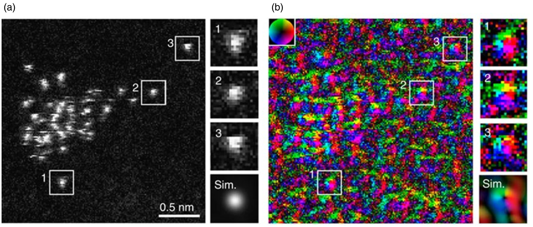
Fig. 14. Simultaneous atomic-resolution ADF STEM image (a) and electric field vector map (b) of Au single atoms. The dwell time is 300 μs per pixel. The inset color wheel indicates how color and shade denote the electric field orientation and strength. Magnified images from three isolated Au atom positions are indicated. Simulated image of a single Au atom supported on a 10 nm-thick amorphous carbon substrate is also shown. Reproduced from Shibata et al. (Reference Shibata, Seki, Sánchez-Santolino, Findlay, Kohno, Matsumoto, Ishikawa and Ikuhara2017).
For thin specimens, the integrated DPC (iDPC) method (Lazić et al., Reference Lazić, Bosch and Lazar2016) possesses advantages for imaging both light and heavy elements (Yücelen et al., Reference Yücelen, Lazić and Bosch2018). The iDPC STEM imaging method was used to detect hydrogen atoms at metal–metal hydride interfaces (de Graaf et al., Reference de Graaf, Momand, Mitterbauer, Lazar and Kooi2020) and subsurface interstitial hydrogen in palladium hydrides (Lin et al., Reference Lin, Wu, Xie, Kang, Du, Kang, Li and Gan2020). For thicker specimens, large illumination angles may enable accurate structure reconstructions of electric potentials by incorporating probe spreading via a multiple plane phase-contrast transfer function (Brown et al., Reference Brown, Ishikawa, Sánchez-Santolino, Shibata, Ikuhara, Allen and Findlay2019). The effect of lens aberrations, electron-beam tilt, and specimen thickness on DPC STEM imaging characteristics was investigated (Buerger et al., Reference Buerger, Riedl and Lindner2020). Understanding of these factors is critical to correctly interpreting and quantifying contrasts in DPC images. Ultrahigh-contrast STEM imaging via high-speed segmented/pixelated detectors by optimum BF (OBF) STEM imaging mode may significantly reduce the electron dose without compromising image resolution (Ooe et al., Reference Ooe, Seki, Ikuhara and Shibata2021). Breakthrough developments in electron detectors, computers, and algorithms significantly advanced the practical realization of imaging technologies.
Coherent versus Incoherent STEM Imaging
The flexibility of STEM imaging provides various approaches to forming images of the sample of interest. Configured STEM detectors, however, can provide entirely different views of the specimen, yielding completely different contrast, resolution limits, and chemical sensitivity. Multiple STEM images can be simultaneously acquired with the same incident electron probe, but the interpretation of these images can be totally different depending on the specific detector size and configuration. For example, when the inner collection angle of the ADF detector increases, the characteristics of the ADF and its corresponding cBF STEM images change from coherent phase contrast to incoherent Z-contrast. For heavy metal atoms supported on ultrathin amorphous carbon films, even low-angle ADF images revealed a certain degree of Z-contrast of metal atoms and demonstrated characteristics of incoherent imaging (Crewe et al., Reference Crewe, Wall and Langmore1970; Wall et al., Reference Wall, Isaacson and Langmore1974a, Reference Wall, Langmore, Isaacson and Crewe1974b; Crewe, Reference Crewe1979, Reference Crewe1983a, Reference Crewe1983b). The very large HAADF detector configurations that were used to image supported metal catalysts also demonstrated characteristics of incoherent imaging (Treacy et al., Reference Treacy, Howie, Pennycook and Mulvey1980; Treacy, Reference Treacy1982; Treacy & Rice, Reference Treacy and Rice1989). The incoherent imaging characteristics include: (1) no contrast reversal with defocus, (2) no interference fringes at interfaces and surfaces, (3) no thickness fringes at crystal wedges, and (4) high atomic number sensitivity. Moreover, the image intensity in an HAADF image of a thin specimen may increase linearly with sample thickness provided that electron-channeling conditions are avoided.
Based on image formation theory, for the same lens systems, incoherent imaging yields higher image resolution than coherent imaging (Scherzer, Reference Scherzer1949). When a zone-axis crystalline specimen is imaged with an ADF detector, the situation becomes dubious: Is the acquired image coherent or incoherent? The question arises about the exact inner angle of the ADF detector for incoherent imaging. Early calculations (Engel et al., Reference Engel, Wiggins and Woodruff1974; Misell et al., Reference Misell, Stroke and Halioua1974) suggested that if the ADF detector collected all of the scattered electrons, then the incoherent imaging characteristics would be displayed. Cowley (Reference Cowley1973a, Reference Cowley1976), however, pointed out that the scattering of high-energy incident electrons by coordinated atoms in a crystalline specimen to an ADF detector might not be a simple summation of independent intensity contributions. Another question arises about the fact that one cannot separate out the scattered electrons from the nonscattered electrons since large convergence angles of the primary electron beam are needed to achieve atomic-resolution imaging. For example, when high-order lens aberrations are corrected, the incident illumination cone may extend to 70–100 mrad even with 200 keV electrons.
Equation (3) discussed in the section “Configured detectors for versatile STEM imaging” is valid as long as the total flux of the incident electrons is preserved. Therefore, the characteristics of ADF images can be understood in terms of the characteristics of the corresponding cBF images provided that the outer angle of the ADF detector is large enough (This assumption implies that the signal strength for electrons scattered at angles larger than the outer angle of the ADF detector is negligible). Since the cBF detector can be considered as the summation of many small detectors with their detector function approaching a delta function, the cBF image intensity can be considered as the summation of the intensity of all the phase-contrast STEM images obtained with such infinitely small BF STEM detectors. The contrast of the cBF and thus the corresponding ADF image is controlled by the sum of all the phase-contrast BF STEM images. Based on the reciprocity principle, a cBF STEM image should be equivalent to a TEM image that is obtained with an incoherently filled illumination aperture, the size of which is determined by the size of the corresponding cBF detector. By analyzing the coherence length of the incoherently filled TEM condenser aperture at the specimen, we can comprehend how a cBF (ADF) STEM image changes from fully coherent to fully incoherent by simply increasing the size of the cBF detector continuously. Furthermore, we will show that in an ADF STEM image, the larger features may be interpreted by an incoherent imaging theory while the smaller features have to be interpreted by a coherent imaging theory. From this perspective, an ultrahigh-resolution ADF STEM image always contains both coherent and incoherent imaging details. For further discussions on partial coherent imaging in scanning microscopes and the effects of detector sizes, the reader should consult relevant publications (Burge & Dainty, Reference Burge and Dainty1976; Fertig & Rose, Reference Fertig and Rose1977; Sheppard & Wilson, Reference Sheppard and Wilson1978; Wilson & Carlini, Reference Wilson and Carlini1987).
We assume that the intensity distribution of the detected electrons is uniform on a disk-like cBF detector with a radius uC, corresponding to a collection angle of θC. Such an assumption greatly overestimates the detected intensity at large scattering angles. In practice, the electron intensity at each detector pixel should be determined by the resultant dynamical electron diffraction pattern, which depends on the crystal structure and orientation, thickness of the specimen, electron probe characteristics, and so on. With the use of such a simplified model, one can, however, easily estimate the widths of transverse coherence/incoherence present in the cBF and the corresponding ADF STEM images. For an incoherently filled TEM condenser aperture, the incoherence and coherence width at the specimen can be approximated by Xi = λ/θC and XC = λ/(2πθC) (Spence, Reference Spence2013), where θC corresponds to the inner collection angle of the ADF detector or the outer collection angle of the cBF detector. For any specimen features >Xi, the corresponding cBF and ADF STEM images can be approximately interpreted as incoherent imaging. On the other hand, for any specimen features <XC, the ADF and cBF STEM images can be interpreted as coherent imaging. For any features with length scales between these two numbers, the images possess both coherent and incoherent characteristics. To gain an intuitive understanding of this complex nature of STEM images, Figure 15 shows the dependence of the incoherence and coherence width on the cBF detector angle for 100 keV electrons. Without knowing the details of the specimen, these plots provide a lower limit for the coherence and incoherence width in the cBF and ADF STEM images. It is clear that for small cBF detectors (corresponding to small ADF inner detector angles), most of the high-resolution features are due to coherent imaging. On the other hand, for very large cBF detectors (corresponding to large ADF inner detector angles), even sub-Ångstrom features can be interpreted by incoherent imaging theory. Figure 15 also suggests that if a smaller probe size (e.g., ac-STEM probe) is used to improve image resolution, then much larger inner collection angles of the ADF detector have to be used to achieve incoherent imaging. If a very small electron probe is used then by varying the inner detection angle of the ADF detector, the corresponding image changes from primarily coherent imaging to primarily incoherent imaging. Since the reciprocity principle applies to inelastic electron scattering with small energy losses (e.g., phonon excitation), the above discussion is valid for experimentally observed STEM images of thin specimens. With large energy-loss electrons, the inelastically scattered electrons do not coherently interfere. Even though the model we used above is rudimentary, the general concept about coherent/incoherent STEM imaging and how the detector size plays a critical role are illustrated. In fact, the difference between incoherent and coherent imaging for a light microscope was discussed in detail by Rayleigh (Reference Rayleigh1896). When there are no “permanent phase-relations” between the light emitting from different points on the object, incoherent imaging follows. For nonluminous objects, Rayleigh pointed out that the use of a convergent source of illumination, provided by a condenser lens, would result in effective incoherent imaging. The large convergence angle from a condenser lens results in a short transverse coherence width, effectively destroys the coherence between neighboring points and provides a very good approximation to incoherent imaging. Although incoherent imaging provides intuitive image interpretation, it contains less information about the specimen than coherent imaging does.
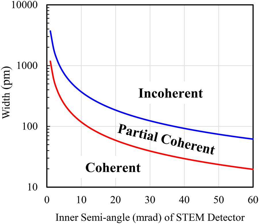
Fig. 15. Calculated dependence of coherence, partial coherence, and incoherence width on the inner semi-collection angle of an ADF detector. The calculation assumed fully coherent and infinitely small incident electron probe and extremely large outer collection angle of the ADF detector. The incoherent nature of image features strongly depends on the feature size and the inner collection angle of the ADF detector.
In practice, both incoherence and coherence width depend on the nature of the specimen: the projected intensity distribution on the STEM detector plane controls the minimum inner detector angle of the ADF detector that provides incoherent imaging characteristics. Since the angular dependence of the scattering cross-section is different for different atomic columns and structures, the incoherence width in an ADF image should be different when the primary electron probe is scanned across the specimen. Generally speaking, the incoherence width is larger for those elements or structures that concentrate the elastic electron scattering to smaller angles. With the use of a thin annular detector, both the coherence and incoherence width increase significantly, leading to partial coherent imaging of high-resolution details. In this case, one can utilize the characteristics of partial coherent imaging to identify the features of interest about the specimen (Cowley, Reference Cowley2001). Digital processing of a series of TAD images can be effectively utilized to gain image contrast and resolution.
Bloch wave and multislice calculations have been extensively carried out to understand the nature of incoherent imaging by the HAADF detector (Pennycook & Jesson, Reference Pennycook and Jesson1990, Reference Pennycook and Jesson1992; Loane et al., Reference Loane, Xu and Silcox1991, Reference Loane, Xu and Silcox1992; Jesson & Pennycook, Reference Jesson and Pennycook1993, Reference Jesson and Pennycook1995; Treacy & Gibson, Reference Treacy and Gibson1993; Amali & Rez, Reference Amali and Rez1997; Nellist & Pennycook, Reference Nellist and Pennycook1999; Nellist et al., Reference Nellist, Pennycook and Kazan2000; Mitsuishi et al., Reference Mitsuishi, Takeguchi, Yasuda and Furuya2001; Muller et al., Reference Muller, Edwards, Kirkland and Silcox2001; Nellist, Reference Nellist2007, Reference Nellist, Pennycook and Nellist2011). The outcome of these extensive studies suggests that the large size of the HAADF detector effectively suppresses transverse (perpendicular to the electron-beam traveling direction) coherence. However, phonon scattering (single plus multiple) is needed to destroy the longitudinal (along the electron beam) coherence. The vibrating atoms only coordinate the movement of its nearest neighbors along a column of atoms of a crystalline specimen and do not have long-range coordination. Therefore, a coherent volume, consisting of “cigar-like” wave packets (Treacy & Gibson, Reference Treacy and Gibson1993), which are narrow in the transverse direction but are highly elongated along the incident beam direction, can be visualized to produce coordinated phonon scattering. Even in thick crystals where dynamical diffraction effects become dominant, the large angular range of the HAADF detector averages out the intensity variations and makes it insensitive to multiple scattering effects. Bloch wave decomposition analyses show that the highly localized 1s state interacts with the atomic nuclei more effectively, resulting in more large-angle scattering events than those of the less tightly bound 2s state. Therefore, interference at large scattering angles between the 1s and 2s states, which produces experimentally observed thickness fringes in BF/DF TEM images, is suppressed (Nellist & Pennycook, Reference Nellist and Pennycook1999; Rafferty et al., Reference Rafferty, Nellist and Pennycook2001; Anstis et al., Reference Anstis, Cai and Cockayne2003). Dynamical diffraction effects still persist since the electron probe does not interact equally with the columns of atoms throughout the sample depth. The HAADF intensity thus monotonically increases with sample thickness but quickly reaches a saturation point due to (1) absorption of the 1s state and (2) broadening of the electron probe as the electrons propagate down the columns of atoms. With a small enough electron probe incident onto a zone-axis crystal, it can be easily observed experimentally that the whole diffraction pattern brightens and “expands” when the electron probe is positioned exactly on the columns of atoms. On the other hand, when the electron probe is positioned at the vacuum channels (between columns of atoms), the intensity of the scattered electrons drops significantly. This is the origin of the “intuitive interpretation” of atomic-resolution Z-contrast STEM images of very thin specimens. When the effective sample thickness increases, such an intuitive interpretation of Z-contrast ADF images may not be valid. For thin specimens, both Bloch wave and multislice simulations yield similar results (LeBeau & Stemmer, Reference LeBeau and Stemmer2008; LeBeau et al., Reference LeBeau, Findlay, Allen and Stemmer2008, Reference LeBeau, D'Alfonso, Findlay, Stemmer and Allen2009a, Reference LeBeau, Findlay, Wang, Jacobson, Allen and Stemmer2009b). For thicker samples, however, the Bloch wave method underestimates the intensity since it does not fully account for the effects of phonon scattering which can play a dominant role in determining the signal strength of the high-angle scattered electrons. Multislice calculations, based on the frozen-phonon model, suggest that when a small electron probe is positioned at an atom column of a zone-axis crystal, the strength of the thermal diffuse scattering is much higher than when the electron probe is positioned between the atom columns. Therefore, the HAADF detector collects not only the Rutherford-scattered electrons but also a large proportion of high-angle phonon-scattered electrons, especially for thicker crystals or specimens at high temperatures.
Electron-Beam Channeling and Atomic Focuser in STEM
Channeling of a charged particle in a crystalline solid refers to the process that the strong interaction of a charged particle with the crystal field of a specimen constrains the propagation of the charged particle along a preferred crystallographic direction (Robinson & Oen, Reference Robinson and Oen1963; Lindhard, Reference Lindhard1965; Gemmell, Reference Gemmell1974). Channeling phenomena and its induced effects reflect the nature of charged particle interactions with crystalline materials. Electron channeling in crystalline samples have long been investigated (Coates, Reference Coates1967; Kreiner et al., Reference Kreiner, Bell, Sizmann, Harder and Hüttl1970; Uggerhøj & Frandsen, Reference Uggerhøj and Frandsen1970; Kambe et al., Reference Kambe, Lehmpfuhl and Fujimoto1974; Komaki & Fujimoto, Reference Komaki and Fujimoto1974; Joy et al., Reference Joy, Newbury and Davidson1982). Contrary to positively charged particles, Rutherford scattering events increased for electrons moving parallel to a zone axis (axial channeling) or a net plane (planar channeling) (Uggerhøj & Frandsen, Reference Uggerhøj and Frandsen1970). Under channeling conditions, incident electrons concentrate on the columns of nuclei and those electrons eventually suffer a high-angle Rutherford scattering or energy-loss events, resulting in a dechanneling process. For thicker samples, re-channeling may occur at the same atomic column or at a nearby atomic column (cross-talking).
Electron channeling affects the collected signal strength of both scattered electrons and emitted particles. Electron channeling modifies image contrast in atomic-resolution STEM images, especially the visibility of single-atom dopants or adatoms (Loane et al., Reference Loane, Kirkland and Silcox1988; Voyles et al., Reference Voyles, Muller, Grazul, Citrin and Gossmann2002, Reference Voyles, Grazul and Muller2003; Rossouw et al., Reference Rossouw, Allen, Findlay and Oxley2003). Channeling of electrons around columns of nuclei can significantly modify the emitted or inelastically scattered signals due to the crystal orientation dependence of electron interaction with the specimen atoms (Spence & Tafto, Reference Spence and Tafto1983; Pennycook & Narayan, Reference Pennycook and Narayan1985; Rossouw et al., Reference Rossouw, Allen, Findlay and Oxley2003; Lugg et al., Reference Lugg, Neish, Findlay and Allen2014, Reference Lugg, Forbes, Findlay and Allen2015a, Reference Lugg, Kothleitner, Shibata and Ikuhara2015b; Allen et al., Reference Allen, Findlay, Oxley, Witte and Zaluzec2006; Kotula et al., Reference Kotula, Klenov and Von Harrach2012; MacArthur et al., Reference MacArthur, Brown, Findlay and Allen2017). For atomic-resolution imaging, electron channeling can be beneficial since it facilitates focusing of a highly convergent STEM probe onto a given atomic column, producing an enhanced ADF signal (Rossouw et al., Reference Rossouw, Allen, Findlay and Oxley2003). Such electron-channeling effects, however, pose significant problems for implementing confocal STEM imaging to provide three-dimensional images of crystals, since the channeled electrons may stay along the atomic column for a relatively large distance (Borisevich et al., Reference Borisevich, Lupini and Pennycook2006; Cosgriff & Nellist, Reference Cosgriff and Nellist2006). Even for small electron probes formed with very large incident beam convergence angles, which are practical on an ac-STEM and are desired for 3D STEM confocal imaging (Ishikawa et al., Reference Ishikawa, Lupini, Hinuma and Pennycook2015, Reference Ishikawa, Pennycook, Lupini, Findlay, Shibata and Ikuhara2016; Nellist, Reference Nellist2017), channeling effects may still pose a problem. For imaging polycrystalline specimens, the channeling effects can mess up the Z-contrast in HAADF images, especially for relatively thicker crystalline materials of heavy elements. In this case, one may be able to differentiate the Z-contrast from channeling contrast by acquiring a pair of images with a slight tilt of the specimen orientation: The channeling contrast is more sensitive to specimen orientation than the Z-contrast, especially for electron probes with relatively small convergence angles.
Channeling effects cannot be avoided in STEM images of polycrystalline thin films regardless of detector angle since the signal strength of even backscattered electrons strongly depends on the orientation of a crystalline specimen. Depending on the specimen thickness, the change in signal strength in an HAADF image can be significant between on-channeling and off-channeling conditions. Diffuse scattering and channeling–dechanneling contrast were used to investigate defects in crystalline specimens (Cowley & Huang, Reference Cowley and Huang1992; Liu & Cowley, Reference Liu, Cowley, Bailey, Bentley and Small1992; Perovic et al., Reference Perovic, Howie and Rossouw1993a, Reference Perovic, Rossouw and Howie1993b; Amali et al., Reference Amali, Rez and Cowley1997). When a crystal is oriented for incident electrons to channel along atomic columns, distortion of the lattice by the defect-induced strain field or the presence of any other heterogeneous entities (surfaces, interfaces, dopants, vacancies, etc.) may de-channel the electrons, leading to detectable darker contrast in ADF images. Based on electron de-channeling interpretation model, the ADF image contrast originates from any types of processes that disrupt electron-channeling conditions. On the other hand, if a crystal is oriented just slightly off the electron-channeling condition, then the strain field around a defect may induce channeling of the electron beam, leading to brighter image contrast in ADF images. Based on these discussions, defects can appear dark, bright, or even invisible in ADF images of zone-axis crystals. Huang scattering (Huang, Reference Huang1947) caused by static displacements of atoms in crystals, as well as channeling-induced scattering both contribute to the collected ADF signal. At very high scattering angles (e.g., HAADF imaging), the channeling or de-channeling contrast dominates (Wang, Reference Wang1994; Grillo et al., Reference Grillo, Mueller, Volz, Glas, Grieb and Rosenauer2011; Phillips et al., Reference Phillips, De Graef, Kovarik, Agrawal, Windl and Mills2012). The contrast features of dislocations depend on both the inner angle of the ADF detector and the depth location of the defects within a specimen (Oveisi et al., Reference Oveisi, Spadaro, Rotunno, Grillo and Hébert2019). Electron channeling and de-channeling effects in crystalline specimens can be effectively utilized to facilitate investigations of interface or surface structures (Yu et al., Reference Yu, Muller and Silcox2008; Grillo, Reference Grillo2009a, Reference Grillo2009b; Liu & Allard, Reference Liu and Allard2010; Grieb et al., Reference Grieb, Müller, Fritz, Grillo, Schowalter, Volz and Rosenauer2013). For plan-view imaging of interfaces, multilayers, precipitates, dopants or supported metal atoms and clusters, electron-channeling effects can be used to enhance visibility of on-column atoms while it suppresses the contrast from atoms sitting between the atomic columns of a crystalline support (Kourkoutis et al., Reference Kourkoutis, Parker, Vaithyanathan, Schlom and Muller2011). Such channeling effects can overshadow the Z-contrast and therefore should be avoided if one desires to interpret an HAADF image as Z-contrast image.
Dynamical diffraction of electrons can be described in real space by considering the fact that electrons are trapped in the electrostatic potential of the atomic columns of a zone-axis crystal (Van Dyck & Op de Beeck, Reference Van Dyck and Op de Beeck1996). The interaction of such channeling electrons with the atomic potential of the specimen leads to dynamical diffraction effects. The wave of the channeling electrons inside a zone-axis crystal was proposed to be compressed to subatomic dimensions along the atomic columns (Fertig & Rose, Reference Fertig and Rose1981). Under certain conditions, the interaction of the high-energy electrons with the crystalline specimen can be treated as if they interact with individual columns of atoms. Cowley et al. (Reference Cowley, Spence and Smirnov1997) realized that when a small STEM probe was channeled along columns of atoms, the electron probe was “focused” by the electrostatic fields of the atoms to produce a much smaller probe which would persist after the electrons exited the specimen. In fact, calculations (Cowley et al., Reference Cowley, Spence and Smirnov1997) suggested that even a heavy single atom could act as a focusing lens (atomic focuser) to produce smaller electron probes (Fig. 16). Thin crystals of high-Z elements were proposed to have a significant focusing effect. A zone-axis thin crystal of a heavy metal could channel a small STEM probe to produce a sharply peaked electron beam outside the exit surface of the crystal, focusing a 0.2 nm initial probe down to ~0.05 nm via a gold atomic focuser (Cowley et al., Reference Cowley, Spence and Smirnov1997). Although such an approach to ultrahigh image resolution may work in theory, there exist practical difficulties due to fast broadening of an electron probe propagating through vacuum. Various imaging modes and designs on how to realize such an ultrahigh-resolution imaging scheme were proposed (Cowley et al., Reference Cowley, Spence and Smirnov1997; Sanchez & Cowley, Reference Sanchez and Cowley1998; Dunin-Borkowski & Cowley, Reference Dunin-Borkowski and Cowley1999; Cowley, Reference Cowley2000; Cowley & Hudis, Reference Cowley and Hudis2000; Smirnov & Cowley, Reference Smirnov and Cowley2002).
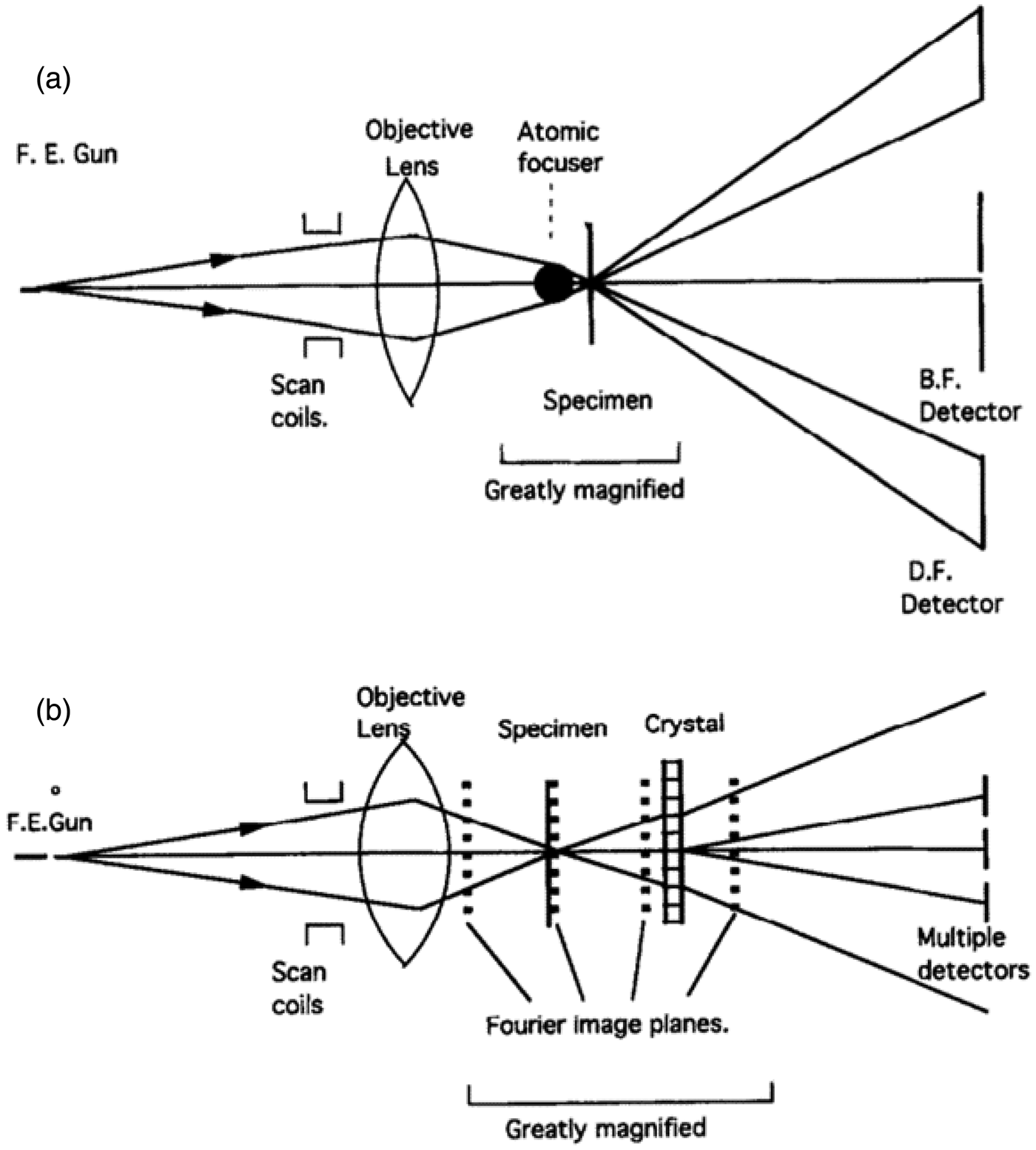
Fig. 16. Schematic diagrams illustrate the STEM imaging with a single atomic focuser (a) and with a thin single crystal, making use of the virtual Fourier images (b). Adapted from Cowley et al. (Reference Cowley, Spence and Smirnov1997).
Both elastic and inelastic electron scattering at a particular location along an atomic column strongly depend on the spatial distribution of the probe intensity profile. Electron-channeling-induced oscillations of STEM probe intensity directly affect many types of collected signals such as emitted X-rays, electron energy-loss events, and electrons scattered into an ADF or BF detector. Understanding the electron-channeling behavior is critical to conducting quantitative analysis of STEM images and spectroscopy data. Detailed calculations (Wu et al., Reference Wu, Mittal, Odlyzko and Mkhoyan2017) suggested that low-Z elements would not have much focusing effect while high-Z elements would act as excellent atomic focusers. Furthermore, the authors concluded that the propagation of the channeling electrons would be strongly regulated by the dynamic angular distribution of the traveling electron probe. Therefore, the nature of the specimen and the characteristics of the incident electron probe control how the channeling electrons produce the various types of scattered and emitted signals. Simulations of electron channeling at a subatomic length scale (Jeong et al., Reference Jeong, Song, Held and Mkhoyan2019) demonstrated that subatomic channeling of high-energy electrons could occur and such electron-channeling effects could even produce helicon-type electron beams (Fig. 17). The helicon-type electron beams may have the potential for probing electronic orbitals of atoms and for measuring magnetic properties of individual atomic columns. The subatomic channeling condition is different from that for on-column channeling. The frequency of the oscillating waves depends on the probe position relative to the center of the atomic column and its atomic number (Jeong et al., Reference Jeong, Song, Held and Mkhoyan2019). The behavior of electron channeling across hetero-interfaces and multilayers controls the image contrast of interfacial misfit dislocation networks in STEM-based images (Perovic et al., Reference Perovic, Howie and Rossouw1993a, Reference Perovic, Rossouw and Howie1993b; Kourkoutis et al., Reference Kourkoutis, Parker, Vaithyanathan, Schlom and Muller2011; Oveisi et al., Reference Oveisi, Spadaro, Rotunno, Grillo and Hébert2019). The interpretation of HAADF-STEM images of overlapping crystals can become quite complicated since the image appearance and contrast depend on a variety of electron optical and specimen parameters (Yun et al., Reference Yun, Prakash, Jalan, Jeong and Mkhoyan2020).
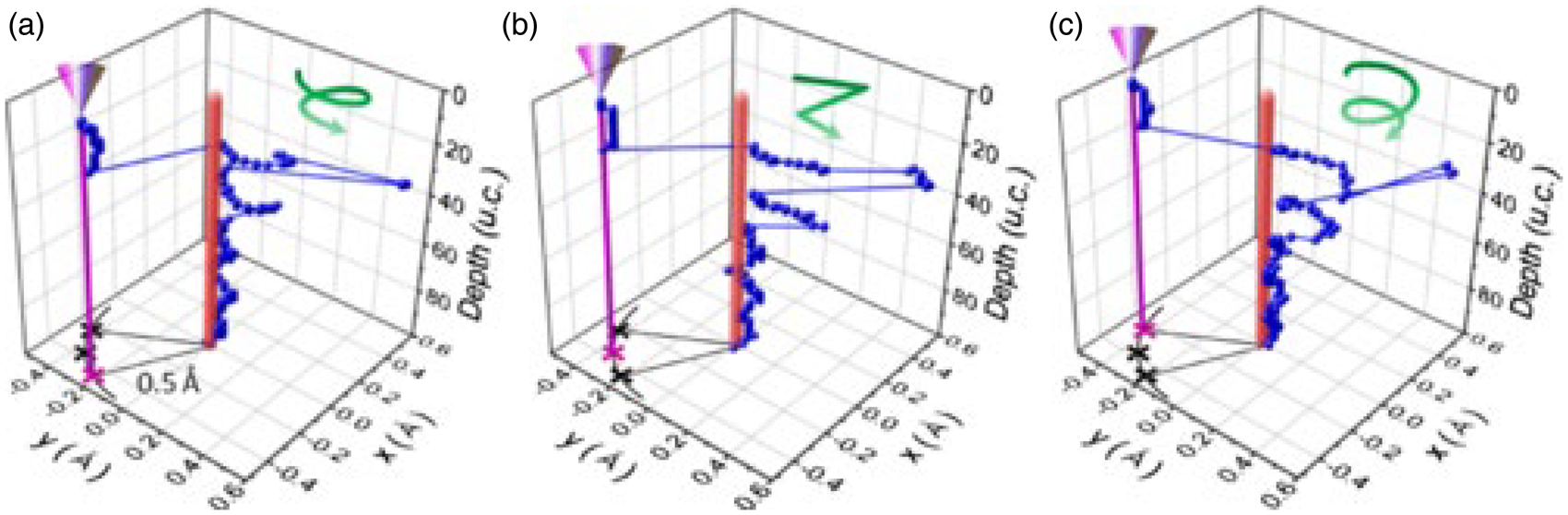
Fig. 17. The formation of a helicon-type beam around the O atomic column in the SrTiO3 crystal. The paths of the electron beams are represented by the maximum intensity positions for the electron probe located at different positions R1 (a), R2 (b), and R3 (c). In all three cases, the probe is located 0.5 Å away from the O atomic column. R1 and R3 are located slightly off the border line, which connects two close O columns in the unit cell, and R2 is located on that line. The probe positions and O atomic column are indicated by the magenta and red vertical lines, respectively. Positions R1 and R3 produce helicon-type beams with opposite chirality, and position R2 produces an oscillating beam. Reproduced from Jeong et al. (Reference Jeong, Song, Held and Mkhoyan2019).
The atomic focusing model of an atom or a column of atoms was used to predict electron scattering cross-sections of heterogeneous materials (van den Bos et al., Reference van den Bos, De Backer, Martinez, Winckelmans, Bals, Nellist and Van Aert2016). For a zone-axis-oriented crystalline specimen, the electron wave passes successive atomic focuser, producing an oscillating probe intensity that depends on the atomic number of the focusing atoms, the atom spacing along the column, the nature of the surrounding atomic columns, and the thermal vibration of the individual atoms. De-channeling can occur, for example, due to scattering by phonons and/or impurity atoms, vacancies, or other types of defects. An atomic lensing model was developed for quantitatively evaluating the 3D structure of Au@Ag core–shell nanorods (van den Bos et al., Reference van den Bos, De Backer, Martinez, Winckelmans, Bals, Nellist and Van Aert2016) and mixed elements within columns (van den Bos et al., Reference van den Bos, Janssens, De Backer, Nellist and Van Aert2019). The use of such an atomic focuser model facilitated atom-counting in heterogeneous nanocrystals. With detailed image simulation and matching with experimental results, it was proposed that the lensing effect of an atom would be independent of electron-beam defocus. Such a method, however, may not be reliable for studying thicker samples and further investigations are needed before such a complicated image interpretation mechanism can be broadly implemented. Although an HAADF imaging mode is preferred for obtaining quantitative information about the specimen of interest, the lensing method also provided valuable information when low-angle ADF (LAADF) and medium-angle ADF (MAADF) imaging modes were employed (van den Bos et al., Reference van den Bos, Janssens, De Backer, Nellist and Van Aert2019).
Nanodiffraction, Ronchigram, Ptychography, and 4D-STEM
When an STEM probe is positioned at any point of a specimen, a CCD camera can capture all the transmitted electrons in the detector plane and, depending on post-specimen lens settings, display part or the whole scattering pattern. The characteristics of the collected diffraction pattern strongly depend on the size of the probe-forming aperture and electron-beam focus. When a small probe-forming aperture is used and the electron probe focuses at a crystalline specimen, a CBED pattern is formed. Such diffraction patterns were traditionally called microdiffraction or nanodiffraction patterns because the diffracted electrons originate from a specimen area of the size of the electron probe (Cowley, Reference Cowley1979a, Reference Cowley1980, Reference Cowley1981a, Reference Cowley1981b, Reference Cowley1982, Reference Cowley1984a, Reference Cowley1984b, Reference Cowley1984c, Reference Cowley1999, Reference Cowley2004; Cowley & Ou, Reference Cowley and Ou1989). The size of the nanodiffraction disk in the detector plane is proportional to the incident beam convergence angle. When a very small incident beam convergence angle is used, leading to large electron probe size due to diffraction effect, the observed electron diffraction patterns resemble those of selected area diffraction patterns in TEM. Structural analyses of small nanoparticles, precipitates, line defects, and so on, can be accomplished by combining STEM imaging with nanodiffraction (Zhu & Cowley, Reference Zhu and Cowley1982; Pan et al., Reference Pan, Cowley and Chan1990; Liu, Reference Liu2005). The diffraction spot splitting/streaking at surfaces/interfaces, due to coherent interference, was evaluated (Liu et al., Reference Liu, Pan and Spinnler1993b; Gajdardziska-Josifovska et al., Reference Gajdardziska-Josifovska, Weiss and Cowley1995; Liu, Reference Liu2005).
When the size of the probe-forming aperture increases, diffracted and transmitted disks broaden and can overlap, yielding interference effects among the transmitted and diffracted electrons. When the probe-forming aperture is completely removed or very large, all the diffraction disks overlap with each other and with the transmitted disk, forming a highly distorted projection (shadow) image of the specimen (Cowley, Reference Cowley1979a). When the electron beam is highly defocused, the shadow-image resembles a low magnification TEM image. If a crystalline specimen is examined, then the close-to-focus shadow image consists of many sets of 1D or 2D fringes which can be highly distorted due to lens aberrations. Since the image characteristics of crystalline shadow images are similar to those observed in light optics for measuring lens aberrations by Ronchi (Reference Ronchi1964), Cowley coined the term electron Ronchigram for describing such shadow images (Cowley, Reference Cowley1980). The axial aberrations of a probe-forming lens are directly visible in a Ronchigram of either a crystalline or an amorphous specimen. The appearance of an electron Ronchigram depends sensitively on probe defocus, astigmatism, spherical aberration coefficient, and the alignment of the electron optical system. Cowley described the electron Ronchigram by considering a transfer function and the projected potential of a specimen (Cowley, Reference Cowley1976, Reference Cowley1979a, Reference Cowley1986). The measurement of aberration parameters of the probe-forming lens can be accomplished by using a focal series of Ronchigrams and simulations (Lin & Cowley, Reference Lin and Cowley1986a, Reference Lin and Cowley1986b; Wong et al., Reference Wong, Kirkland, Xu, Loane and Silcox1992; Wang & Cowley, Reference Wang and Cowley1995; Ramasse & Bleloch, Reference Ramasse and Bleloch2005; Yamazaki et al., Reference Yamazaki, Kotaka, Kikuchi and Watanabe2006; Lupini & Pennycook, Reference Lupini and Pennycook2008; Kimoto & Ishizuka, Reference Kimoto and Ishizuka2017).
When an amorphous region is under STEM probe illumination, the angular distribution of the scattered electrons is mostly located within the transmitted disk (large or no probe-forming aperture) and diffraction beams are hardly discernible in the electron Ronchigram. When the electron beam is far out-of-focus, the projection image resembles a conventional BF TEM image of amorphous materials. As the defocus value is decreased, both the shadow-image magnification and distortion increases significantly. Explanations for these experimentally observed phenomena were discussed in detail (Cowley, Reference Cowley1979a, Reference Cowley1986; Lupini, Reference Lupini, Pennycook and Nellist2011). The electron Ronchigram from an amorphous region provides a convenient approach to aligning STEM electron optical components, correcting for astigmatism and coma, adjusting probe defocus, and selecting/centering the probe-forming aperture (Cowley, Reference Cowley1979b; James & Browning, Reference James and Browning1999; Dellby et al., Reference Dellby, Krivanek, Nellist, Batson and Lupini2001; Liu, Reference Liu2005; Yamazaki et al., Reference Yamazaki, Kotaka, Kikuchi and Watanabe2006; Fig. 18). A Ronchigram can be conveniently used to extract aberration parameters of the imaging system and/or to auto-tune the probe-forming lens system (Krivanek et al., Reference Krivanek, Dellby and Lupini1999; Dellby et al., Reference Dellby, Krivanek, Nellist, Batson and Lupini2001; Lupini et al., Reference Lupini, Wang, Nellist, Kirkland and Pennycook2010). By using autocorrelation function of a segmental Ronchigram to measure the aberration parameters, Sawada et al. developed a method to automatically determine lens aberrations up to the fifth order (Sawada et al., Reference Sawada, Sannomiya, Hosokawa, Nakamichi, Kaneyama, Tomita, Kondo, Tanaka, Oshima, Tanishiro and Takayanagi2008). The electron Ronchigram method is extremely useful for fast searching sample regions of interest, for STEM alignment, for selecting and centering the probe-forming aperture, and for orienting crystalline specimens via the Kikuchi line method (Levine et al., Reference Levine, Bell and Thomas1966; Smith & Cowley, Reference Smith and Cowley1971).
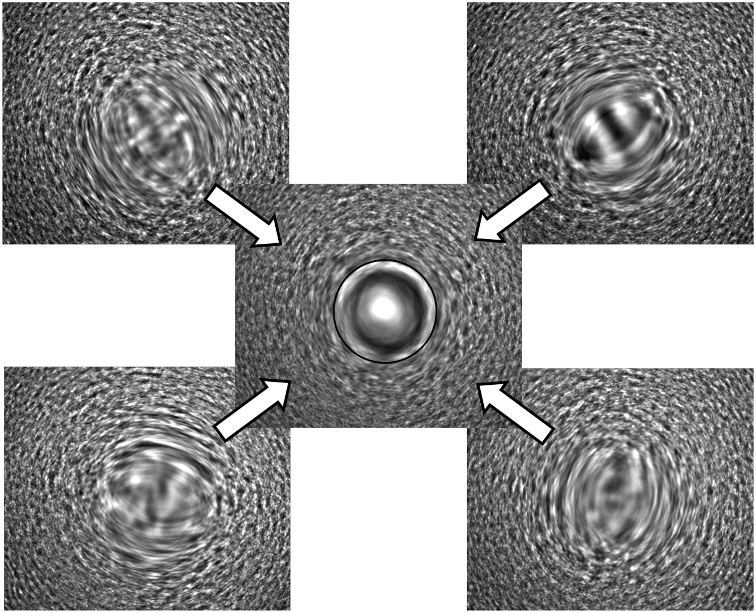
Fig. 18. A set of shadow images of an amorphous carbon film illustrates the use of shadow images to correct the astigmatism of the probe-forming lens, to find the coma-free optical axis, to determine the defocus value of the electron beam, and to auto-tune the aberration corrector settings. Reproduced from Liu (Reference Liu2005).
When the probe-forming aperture allows diffraction disks to overlap, the probe may become small enough to resolve the corresponding lattice fringes in ADF images provided that lens aberrations are small enough. At each fixed probe position, the coherent CBED pattern contains all the information about the specimen. Lens aberrations, however, impose distortions on such CBED patterns (Cowley, Reference Cowley1984a, Reference Cowley1984b, Reference Cowley1984c, Reference Cowley1986; Lin & Cowley, Reference Lin and Cowley1986a, Reference Lin and Cowley1986b; Cowley & Ou, Reference Cowley and Ou1989). Without the use of aberration correctors, electron nanodiffraction patterns could be obtained using electron probes as small as 0.3 nm in diameter and such diffraction patters could be stored on a video tape at a rate of 30 patterns/s (Cowley, Reference Cowley1984a, Reference Cowley1984b, Reference Cowley1984c). Cowley proposed that by analyzing these coherent CBED patterns, which would change appreciably when the electron beam was translated by a small fraction of the probe diameter, information on the structure of the probed atoms within the electron beam with a resolution much smaller than the probe size would be obtainable. Cowley stated that a super-resolution down to 0.05 nm, with a 0.3 nm electron probe, would be achievable by properly processing the recorded nanodiffraction patterns. Theoretical calculations, via tracking the intensity of Patterson components in the nanodiffraction plane to determine the interatomic vectors corresponding to pairs of atoms under probe illumination, showed the feasibility of such an approach (Konnert & D'Antonio, Reference Konnert and D'Antonio1986). Theoretical considerations and comparisons to experimental results demonstrated that an image resolution approaching 0.1 nm was achievable (Konnert et al., Reference Konnert, D'Antonio, Cowley, Higgs and Ou1989). This approach, however, relied on having sufficient a priori information about the structure being examined. Although these earlier efforts demonstrated the feasibility for resolution improvement, the lack of appropriate high-quality electron detectors and data storage systems, faster computers, and better algorithms made such an approach not practical.
During the same time period when Cowley focused on improving image resolution via processing nanodiffraction patterns and in-line holograms (Cowley, Reference Cowley1979a, Reference Cowley1979b, Reference Cowley1979c, Reference Cowley1979d; Lin & Cowley, Reference Lin and Cowley1986a, Reference Lin and Cowley1986b; Cowley, Reference Cowley1990, Reference Cowley1992), Rodenburg emphasized extracting useful information on both crystalline and amorphous materials via analysis of nanodiffraction patterns by developing new algorithms (Rodenburg & McMullan, Reference Rodenburg and McMullan1985; Rodenburg, Reference Rodenburg1988, Reference Rodenburg1989). Rodenburg and Bates (Reference Rodenburg and Bates1992) published a paper on employing the Wigner-distribution deconvolution approach to achieving super-resolution. By use of the Wigner-distribution function, the instrument parameters were entirely separated from the specimen information. In theory, the extracted specimen function should possess a spatial resolution approaching the electron wavelength. The final reconstructed image was shown to be insensitive to specimen thickness and partial coherence of the electron beam, and tolerance to certain levels of noise. In this paper, the authors used the word “ptychography,” following the earlier designation (Hegerl & Hoppe, Reference Hegerl and Hoppe1970, Reference Hegerl, Hoppe and Glauert1972), to differentiate this approach from electron holography. With a TV rate CCD camera to record nanodiffraction patterns, Rodenburg and colleagues demonstrated the practicality and the feasibility of significantly improving image resolution via processing of coherent CBED (Rodenburg et al., Reference Rodenburg, McCallum and Nellist1993; Nellist et al., Reference Nellist, McCallum and Rodenburg1995). These authors were able to extract phase differences among all the neighboring pairs of diffracted beams in a coherent CBED, and an image resolution of <0.14 nm was achieved from an STEM instrument with a conventional point resolution of 0.42 nm. Further improvement in the phase retrieval algorithm made the ptychography approach more robust (Maiden & Rodenburg, Reference Maiden and Rodenburg2009).
The next breakthrough in realizing significantly improved image resolution was detector development. Ideally, one desires an electron detector that possesses ultrahigh sensitivity (e.g., for low-dose applications), ultrafast speed readout, and ultrahigh dynamic range. The detector must read out fast to reduce adverse effects of sample drift, electron-beam-induced effects, and other types of disturbances. To reconstruct an image of a reasonable area of a specimen with high image resolution, the detector should possess a reasonable number of pixels (e.g., 512 × 512 or 1,024 × 1,024 pixels) and each coherent CBED should be acquired in a short time. The coupling of a scintillator with a CCD for digital readout has good electron sensitivity but suffers readout speed (about 30–60 frames/s for most applications) and has a limited dynamic range (Fan & Ellisman, Reference Fan and Ellisman1993; De Ruijter, Reference De Ruijter1995). The development of monolithic active pixel sensors (APSs), employing complementary metal-oxide-semiconductor (CMOS) chips, made it possible to have very high sensitivity and fast readout speed (Mendis et al., Reference Mendis, Kemeny, Gee, Pain, Staller, Kim and Fossum1997; McMullan et al., Reference McMullan, Faruqi, Clare and Henderson2014). The disadvantage of the APS-based electron detectors is that they possess a relatively poor dynamic range. Another major advance in detector technology was the development of hybrid pixel array detector (PAD) which used arrays of photodiodes and application-specific integrated circuits (Ansari et al., Reference Ansari, Beuville, Borer, Cenci, Clark, Federspiel, Gildemeister, Gössling, Hara, Heijne, Jarron, Lariccia, Lisowski, Munday, Pal, Parker, Redaelli, Scampoli, Simak, Singh, Vallon-Hulth and Wells1989; Caswell et al., Reference Caswell, Ercius, Tate, Ercan, Gruner and Muller2009), providing fast readout speed, high dynamic range, and single electron counting sensitivity (Tate et al., Reference Tate, Purohit, Chamberlain, Nguyen, Hovden, Chang, Deb, Turgut, Heron, Schlom, Ralph, Fuchs, Shanks, Philipp, Muller and Gruner2016).
With the use of these new types of electron detectors, robust algorithms for data processing, and faster computers, impressive results firmly established the power of ptychography approach to super-resolution imaging. For example, an image resolution of 39 pm was achieved (at 80 kV) on a 2D molybdenum disulfide (MoS2) sample, far exceeding the conventional imaging resolution of 98 pm for these microscope parameters (Jiang et al., Reference Jiang, Chen, Han, Deb, Gao, Xie, Purohit, Tate, Park, Gruner, Elser and Muller2018; Fig. 19). With such an image resolution, the atomic arrangement of a crystal as well as defect structures within the crystal may become clearly discernible. The authors also conducted simulations and concluded that defocused-probe iterative ptychography outperforms both focused-probe iterative ptychography and the Wigner-distribution deconvolution method by approximately a factor of 2 in signal-to-noise improvement. The success of ptychography approach to ultrahigh-resolution imaging encouraged broad applications to solving various types of material problems (Yang et al., Reference Yang, Rutte, Jones, Simson, Sagawa, Ryll, Huth, Pennycook, Green, Soltau, Kondo, Davis and Nellist2016, Reference Yang, MacLaren, Jones, Martinez, Simson, Huth, Ryll, Soltau, Sagawa, Kondo, Ophus, Ercius, Jin, Kovács and Nellist2017a; Wang et al., Reference Wang, Zhang, Gao, Zhang and Kirkland2017; dos Reis et al., Reference dos Reis, Yang, Ophus, Ercius, Bizarri, Perrodin, Shalapska, Bourret, Ciston and Dahmen2018; Lozano et al., Reference Lozano, Martinez, Jin, Nellist and Bruce2018; Fang et al., Reference Fang, Wen, Allen, Ophus, Han, Kirkland, Kaxiras and Warner2019).
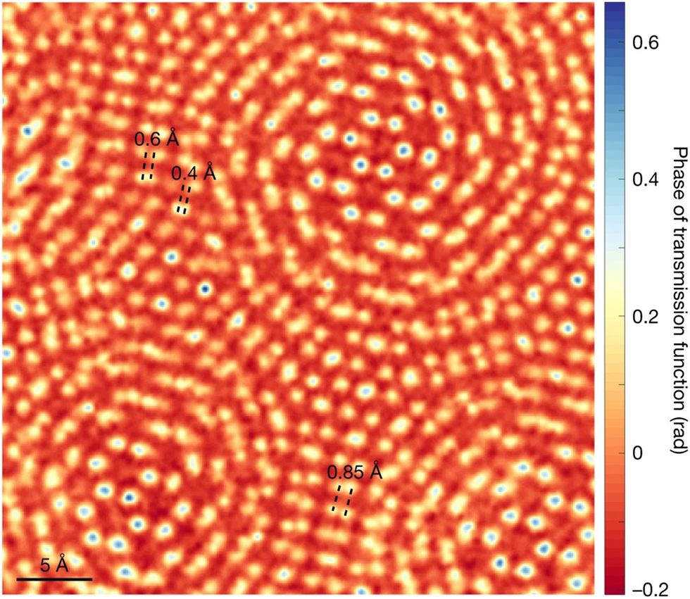
Fig. 19. Real-space resolution test of full-field ptychography using twisted bilayer MoS2.The two sheets are rotated by 6.8° with respect to each other, and the mis-registration of the molybdenum atoms provides a range of projected distances that vary from a full bond length down to complete overlap. Atoms are cleanly resolved at a separation of 85 ± 2 pm, with a small dip present between atoms separated by ~61 ± 2 pm. Atom-pair peaks at 42 ± 2 pm show a 6% dip at the midpoint, suggesting that the Sparrow limit lies just below 40 pm. The Raleigh resolution for the ADF STEM is 120 pm for these imaging conditions. Reproduced from Jiang et al. (Reference Jiang, Chen, Han, Deb, Gao, Xie, Purohit, Tate, Park, Gruner, Elser and Muller2018).
With commercially available fast pixelated direct electron detectors, focused-probe ptychography can be routinely accomplished, although real-time ptychography is not possible yet. The high sensitivity of pixelated electron detectors makes it possible to practice low-dose electron microscopy which is critical to significantly expanding practical applications of ac-STEM to studying electron-beam-sensitive materials and systems. Determining the local atomic arrangement of complex nanostructures of electron-radiation-sensitive materials has always been a grand challenge. Generally speaking, the required illumination dose for electron optical imaging is approximately inversely proportional to the square of spatial resolution (Saxberg & Saxton, Reference Saxberg and Saxton1981). Therefore, much higher electron doses are needed to improve image resolution. For electron-beam-sensitive materials, however, higher electron doses may destroy the specimen structure before a reasonable quality image can even be acquired. Since electron ptychography utilizes the information contained in the whole diffraction pattern, it offers the possibility of extremely low-dose imaging of electron-beam-sensitive materials with atomic-resolution, rivaling that of cryo-TEM methods. It has been demonstrated that by using a mixed-state reconstruction algorithm, the mixed-state ptychographic approach could reduce electron doses by 50 times while still maintaining the image resolution and large field of view (Chen et al., Reference Chen, Odstrcil, Jiang, Han, Chiu, Li and Muller2020). With the use of a defocused electron probe, robust ptychography under low-dose conditions was realized (Song et al., Reference Song, Allen, Gao, Huang, Sawada, Pan, Warner, Wang and Kirkland2019). Electron ptychography has significant potential for applications in structure determination of biological samples, especially when it is conducted on samples at cryogenic temperatures (Zhou et al., Reference Zhou, Song, Kim, Pei, Huang, Boyce, Mendonça, Clare, Siebert, Allen, Liberti, Stuart, Pan, Nellist, Zhang, Kirkland and Wang2020).
The term “4D-STEM” is used to describe the collection of the whole diffraction pattern from each electron probe position over a specimen area, and the subsequent reconstruction of various types of images from the diffraction dataset (Fig. 20). In fact, as described in the section “Configured detectors for versatile STEM imaging,” ideally one would like to add another dimension of data to the 4D-STEM: for each fixed probe position, each set of diffraction patterns should be recorded with a specific energy loss. The 5D-STEM dataset contains not only structure information in real and reciprocal space but also full information about inelastic scattering events in both real and momentum space. Since 4D-STEM dataset contains all structural information of the specimen virtual experiments can be performed on this dataset to yield all types of images, as discussed in the section “Configured detectors for versatile STEM imaging.” In the late 1980s and early 1990s, Cowley constantly emphasized the rich information stored in each coherent CBED pattern, stored on video tapes, as he manually moved the electron probe across the sample of interest. However, the lack of high-performance electron detectors, data storage media, faster computers, and robust reconstruction algorithms prevented the successful implementation of his excellent ideas.
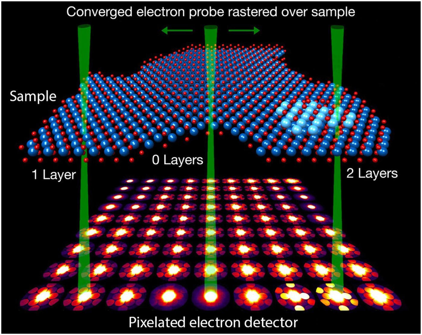
Fig. 20. Experimental 4D-STEM measurement of a dichalcogenide 2D material. The various types of real-space atomic-resolution images can be reconstructed from the diffraction dataset; each diffraction pattern represents an average of 7 × 7 experimental images. Green STEM probes are labeled for regions of the sample with one layer, vacuum, and two layers. The total dataset was acquired in 164 s and contains 420 GB data. The high-speed and efficient direct electron detectors, and the readily available computational power enable such experiments possible. Reproduced from Ophus (Reference Ophus2019).
The rich information contained in a 4D-STEM dataset and its flexibility for providing various types of STEM images have made this method a preferred approach to characterizing a wide variety of materials systems including biological and soft materials. Ophus recently provided a detailed review of this technique including historical development and applications (Ophus, Reference Ophus2019). Since manipulation and processing of 4D-STEM datasets can provide phase-contrast, Z-contrast, strain-field-induced contrast, or other contrast mechanisms, and enable low-dose approach without compromising image resolution, it is expected that 4D-STEM will provide an unparalleled approach to atomic-resolution imaging of materials that previously could not be examined due to electron-beam-induced effects. With a 4D-STEM dataset, one has complete flexibility to apply a virtual mask of any shape or size to produce STEM images of interest (e.g., differential phase contrast or center-of-mass images) to extract relevant information of the specimen (Han et al., Reference Han, Nguyen, Cao, Cueva, Xie, Tate, Purohit, Gruner, Park and Muller2018; Bammes et al., Reference Bammes, Ramachandra, Mackey, Bilhorn and Ellisman2019; Das et al., Reference Das, Tang, Hong, Gonçalves, McCarter, Klewe, Nguyen, Gómez-Ortiz, Shafer, Arenholz, Stoica, Hsu, Wang, Ophus, Liu, Nelson, Saremi, Prasad, Mei, Schlom, Íñiguez, García-Fernández, Muller, Chen, Junquera, Martin and Ramesh2019; Fang et al., Reference Fang, Wen, Allen, Ophus, Han, Kirkland, Kaxiras and Warner2019; Gao et al., Reference Gao, Addiego, Wang, Yan, Hou, Ji, Heikes, Zhang, Li, Huyan, Blum, Aoki, Nie, Schlom, Wu and Pan2019; Müller-Caspary et al., Reference Müller-Caspary, Krause, Winkler, Béché, Verbeeck, Van Aert and Rosenauer2019; Pekin et al., Reference Pekin, Ding, Gammer, Ozdol, Ophus, Asta, Ritchie and Minor2019; Wen et al., Reference Wen, Ophus, Allen, Fang, Chen, Kaxiras, Kirkland and Warner2019; Londoño-Calderon et al., Reference Londoño-Calderon, Williams, Ophus and Pettes2020; Wu et al., Reference Wu, Meng and Zhu2020; Mahr et al., Reference Mahr, Müller-Caspary, Grieb, Krause, Schowalter and Rosenauer2021).
Quantitative Atomic-Resolution STEM Imaging
The measurement of the positions of individual atoms in materials with picometer-scale precision is required to understand the structure of surfaces, interfaces, and the various types of defects that control or influence a broad spectrum of materials behavior. X-ray-based methods can provide structural information with such a precision but are averaged over a large volume of the sample of interest. Local structural and chemical information of subnanometer- or nanometer-scale heterogeneities in a sample, however, requires much higher spatial resolution than X-ray-based techniques can provide. STEM-based imaging, spectroscopy, and diffraction techniques can provide atomic-scale information of the specimen with picometer precision provided that the various types of instrument-, specimen-, and environment-related artifacts are alleviated or completely eliminated. With the use of a modern ac-STEM instrument, sub-pm precision and standardless atom-counting with <1 atom uncertainty in STEM images of supported Pt nanoparticles have been realized (Yankovich et al., Reference Yankovich, Berkels, Dahmen, Binev, Sanchez, Bradley, Li, Szlufarska and Voyles2014). Such high-precision, atomic-resolution STEM images are critical to understanding the physicochemical properties of many nanostructured materials and systems. Precise atomic models of nanostructures and systems, based on high-precision STEM imaging, are the foundation for understanding structure–performance relationships and for designing novel nanostructures that possess unique physicochemical properties. For example, Nilsson Pingel et al. (Reference Nilsson Pingel, Jørgensen, Yankovich, Grönbeck and Olsson2018), using an atomic-resolution, high-precision STEM imaging approach, experimentally measured the site-specific strain at interfaces, surfaces, and defects in Pt nanoparticles supported on alumina and ceria. These authors found that the largest strains occurred at the interfaces and were predominantly compressive. By combining the STEM measurements with first-principles kinetic Monte Carlo simulations of CO oxidation reaction, the authors concluded that the presence of only a fraction of strained surface atoms could influence the catalytic turnover frequency for CO oxidation, quantitatively demonstrating the relationship between strain and catalytic function of nanostructures and interfaces.
Correction of Image Distortions and Structural Measurement with Picometer Precision
Unlike parallel imaging systems (e.g., TEM), the formation of a scanning probe microscopy (e.g., STEM) image requires movement of a fine probe across a sample surface in order to form an image. This procedure can introduce various types of artifacts in the image due to the time delay between the signal measurements and the accumulative error in the probe position with respect to the specimen. Examples of such artifacts include linear distortions, random “jitter” of probe position due to various types of interferences, jump discontinuities due to sample instability, random drifting of specimen, and so on. All scanning probe images contain distortions and these distortions are frequently much larger than the atomic-scale features of interest. During the early periods of STEM development, image distortions due to environmental factors could become so severe that crystal lattice fringes looked like random waves in the recorded images. The imaging distortions may originate from mechanical and/or acoustic vibrations, instabilities in power supplies for the lenses or alignment coils, electric/magnetic fields within and/or around the microscope column, computer fans, and so on. In addition to disturbances due to environmental (acoustic, mechanical, and/or electromagnetic) factors, many instrumental factors also affect the accurate measurement of fine structures in an STEM image (von Harrach, Reference von Harrach1995). For atomic-resolution STEM imaging, different parts in a recorded image may be distorted differently and image features may appear “torn” (feature rows shift horizontally), “sliced” (feature rows shift vertically), or “sheared” (image features elongate). The designs of modern ac-STEM instruments have been significantly improved with the goal of reducing the effects of instrument factors on image resolution. The ac-STEM instrument, especially in the shadow-image mode, is the most sensitive device to evaluate microscope- and building-related instabilities. As the spatial resolution of an STEM instrument improved, its sensitivity to room environment became more noticeable and posed a severe limitation to achieving the microscope's high-resolution capabilities. Room design to reduce external interferences became an integral part of a successful installation of an ac-STEM with desired performances. Quantitative characterization of an STEM's response to magnetic, mechanical, acoustical, and thermal disturbances was discussed (Muller et al., Reference Muller, Kirkland, Thomas, Grazul, Fitting and Weyland2006).
An approach to recovering a nondistorted STEM image is correction of scanning distortion with the goal of maintaining accuracy and resolution of the STEM images of interest. Such a post-processing approach proved to be extremely successful in significantly increasing the measurement precision of structural parameters to the picometer scale. Rečnik et al. (Reference Rečnik, Möbus and Šturm2005) used CTEM images as references to correct the corresponding STEM images. This method was applied to extracting compositional atomic-column data from HAADF-STEM images of crystals with local occupancy or chemistry fluctuations, stacking faults, special grain boundaries, or interfaces. Such an image-warp method, however, needs an available structural model. Sanchez et al. (Reference Sanchez, Galindo, Kret, Falke, Beanland and Goodhew2006) developed an algorithm for correcting time-invariant image distortions such as hysteresis effects during “fly back” between scan lines or systematic beam deflections due to external electromagnetic fields. They further successfully applied this method for local strain mapping of heterostructures. Braidy et al. (Reference Braidy, Le Bouar, Lazar and Ricolleau2012) proposed a method, based on phase analysis of streaks in Fourier space, for analyzing and subsequently correcting systematic row displacement errors in STEM images of periodic structures. Jones and Nellist (Reference Jones and Nellist2013) investigated the sources, nature, and effects of imaging distortions and developed an image reconstruction code to restore the majority of detrimental distortion effects on atomic-resolution data. The image restoration protocol was developed on the assumption that the image drift rate and direction during the image acquisition process were constant. In addition to correcting image drift effects, these authors improved image resolution as well as the signal-to-noise ratio. Based on a real-space template matching technique, Zuo et al. (Reference Zuo, Shah, Kim, Meng, Gao and Rouviére2014) developed a quantitative lattice analysis and a scanning distortion-correction protocol. This method uses the template of an atomic column or a group of atomic columns to transform the image into a lattice of correlation peaks. A reference lattice, however, is needed to correct for scan noise and scan distortions in the recorded images.
Berkels et al. (Reference Berkels, Binev, Blom, Dahmen, Sharpley and Vogt2014) proposed a methodology, based on a nonrigid pixel-wise registration method to cope with low signal-to-noise ratios in scanning images, for extracting useful information from a series of STEM images. The success of this strategy is based on: (1) replacing single-frame high-dose data acquisition by several low-dose short exposure frames and (2) properly synthesizing the information from such a series of frames by a novel cascading registration methodology. The multilevel nonrigid registration method, which accurately links the information carried by many sequentially acquired low-dose frames, is the essence of this proposed protocol. The authors applied quantitative objective-quality measures to illustrate the effectiveness of the proposed procedures and successfully applied the method to extract structural information on electron-beam-sensitive siliceous zeolite materials. Sang & LeBeau (Reference Sang and LeBeau2014) developed a protocol called RevSTEM to remove sample drift distortion from atomic-resolution images without the need for a priori crystal structure information. To measure and correct the distortion, a series of fast-acquisition STEM images with rotated scan coordinates need to be acquired. These authors demonstrated that the RevSTEM protocol simultaneously removed the need for a priori structure information to correct distortion, leading to a dramatically improved signal-to-noise ratio, and enabling picometer precision and accuracy regardless of a drift rate. Yankovich et al. (Reference Yankovich, Berkels, Dahmen, Binev, Sanchez, Bradley, Li, Szlufarska and Voyles2014) developed a successful scheme, based on nonrigid registration and averaging over an image series, to achieve extremely high signal-to-noise ratio (SNR) STEM images, providing sub-pm precision in structure measurement and standardless atom-counting with <1 atom uncertainty in STEM images. The authors proved that the nonrigid registration approach achieved five to seven times better precision than the previous image distortion-correction approaches. Berkels & Liebscher (Reference Berkels and Liebscher2019) reported a novel bias-corrected nonrigid registration approach that compensated for both fast and slow scan artifacts in STEM image series. The bias-correction method allows to reduce fast scan noise in an image series and slow scan distortions simultaneously. Such an image-correction process may have applications in atomic-resolution strain and elemental mapping.
During an STEM experiment, many types of samples may be sensitive to electron-beam-irradiation effects (Egerton et al., Reference Egerton, Li and Malac2004; Egerton, Reference Egerton2013, Reference Egerton2019). Therefore, the use of low electron doses and as few measurements as possible to correct image distortions are highly desirable. With this expectation, Ophus et al. (Reference Ophus, Ciston and Nelson2016a) designed a procedure to correct linear and nonlinear distortions by using orthogonal scan pairs to align each measurement line-by-line along the slow scan direction and fitting the contrast variations along the lines. The algorithm requires no a priori assumptions about image features and requires only two images as an input, minimizing acquisition time and electron dose. Bárcena-González et al. (Reference Bárcena-González, Guerrero-Lebrero, Guerrero, Yañez, Nuñez-Moraleda, Fernández-Reyes, Real, González and Galindo2020) further proposed a CDrift algorithm for correcting linear drift from a single atomic-resolution STEM image. This method is based on angle measurements in the Fourier space and an iterative algorithm, based on successive rotation/drift correction steps, is required to remove drift distortions in atomic-resolution STEM images. The general applicability and robustness of this approach need to be evaluated and validated.
When the scanlines are misaligned, distortions occur that degrade the accuracy and precision of which a modern ac-STEM can provide. In general, the slow scan direction is more prone to various types of disturbances. Alternative scanning paths to form images may be used to reduce image distortions. Spiral scanning paths were investigated as an alternative approach to acquiring images at extremely high speed (Sang et al., Reference Sang, Lupini, Unocic, Chi, Borisevich, Kalinin, Endeve, Archibald and Jesse2016, Reference Sang, Lupini, Ding, Kalinin, Jesse and Unocic2017). Different scans with constant angular and linear velocity spirals were evaluated. These exotic scanning methods suffer nonuniform image quality over the scanned area. The sparse acquisition approach, with a goal of reducing electron dose/dose rate to a sample during imaging, can be employed to either alleviate image distortions or to significantly reduce electron dose and/or acquisition time (Kovarik et al., Reference Kovarik, Stevens, Liyu and Browning2016). Other scanning approaches such as “snake” patterning, where the scan direction is reversed after each row, and Hilbert scan patterning that changes scan direction rapidly, were proposed and evaluated (Velazco et al., Reference Velazco, Nord, Béché and Verbeeck2020). The authors demonstrated that the Hilbert scan patterning approach possessed certain advantages for faithfully representing the high-frequency content in an image in the presence of sample drift. Compared with the conventional raster scan with fly-back correction, both the “snake” and Hilbert scanning approach may reduce the required electron dose for similar quality of STEM images.
Quantification of STEM Image Intensities
Qualitative matching between simulated and experimental atomic-resolution images is routine practice with the goal of distinguishing material structures. To fully extract structural and chemical information, such as the number and types of atoms and the precise positions of each atomic species in the specimen of interest, however, requires quantitative comparisons between simulated and experimental STEM images. Since the HAADF signal carries both structural and chemical information of the probed area, it is expected that quantitative analysis of contrast variations and peak intensities in HAADF images may provide atomic-scale information for understanding and establishing structure–performance relationships (Klenov & Stemmer, Reference Klenov and Stemmer2006; Klenov et al., Reference Klenov, Findlay, Allen and Stemmer2007).
Size Determination of Metal Clusters and Particles via Intensity Quantification
In examining heavy metal nanoparticles in supported metal catalysts, Treacy & Rice (Reference Treacy and Rice1989) developed a method to determine the size of small metal particles by quantitatively evaluating the total intensity of a particle in an HAADF-STEM image. They showed that the number of atoms in a small metal cluster could be estimated from the HAADF signal strength and demonstrated that the method would be particularly useful for detecting and measuring particles in the subnanometer size range. The integrated particle intensity was proposed to be proportional to the number of atoms probed by the electron beam, weighted by their individual scattering cross-sections. They further verified, using experimental data, that a straight line would result when the square root of the imaged area (A 1/2) was plotted against the cubic root of intensity (I 1/3). Such plots provide the calibration of the intensity increment per atom without the need of external calibration. A high signal-to-noise ratio and optimum sampling of the specimen are highly desirable for this method to work. By using such an integrated intensity approach, the authors reliably detected Pt clusters of only three atoms even though the STEM probe size was ~0.35 nm. Such a method was applied to quantitative measurement of small Re particles and clusters (Singhal et al., Reference Singhal, Yang and Gibson1997). Statistical measurement of absolute cross-sections of Re-6 clusters showed good agreement with theoretical cross-sections, within a ±2 atom random error. To reduce errors in quantitative measurement, the authors calibrated their ADF detector and paid special attention to reducing the sources of error in absolute intensity measurements. The authors speculated on the possibility of single-atom sensitivity and named this quantification method as STEM-based mass spectroscopy. Yang et al. (Reference Yang, Bradley and Gibson2000) developed a computer program to automatically find the locations of metal clusters in HAADF images and then to integrate the HAADF intensity of each cluster, leading to the determination of the number of atoms in each cluster. The use of automated analysis of image intensities made the STEM mass-spectroscopic technique statistically meaningful and robust. By analyzing the particle area–intensity relationships, the 3D shapes of small metal particles and clusters may be inferred (Treacy & Rice, Reference Treacy and Rice1989). Young et al. (Reference Young, Li, Chen, Palomba, Di Vece and Palmer2008), using size-selected nanoclusters as mass standards, quantified the masses and 3D shapes of supported metal nanoparticles. Through quantitative image intensity analysis, the authors found that the HAADF intensity displays a monotonic dependence on cluster size, even for as many as 6,500 atoms of Au supported on carbon, significantly extending the applicability of the STEM mass-spectrometry method.
Quantitative Atomic-Resolution STEM Imaging and Atom-Counting
In addition to correcting for image distortions, a quantitative evaluation of STEM images requires analysis of contrast variations, measurement of atom positions and peak intensities, and comparisons to calculations. The collected ADF signal, for example, may include Rutherford-scattered electrons, phonon-scattered electrons, electrons scattered by various types of defects, and inelastically scattered electrons. Further considerations in image simulations need to account for detector size, shape, and pixel response; specimen orientation, effects of amorphous layers and strain field; source size broadening and partial coherence; and electron optical parameters (probe size, convergence angle, electron energy, lens aberrations, defocus value, etc.). Among all the imaging modes available in an STEM instrument, the highly intuitive HAADF imaging mode is of special interest because it provides high chemical sensitivity with ultimate spatial resolution. The experimentally measured image intensity of an HAADF image is a function of atomic number and the number of atoms covered by the incident electron probe. A quantitative interpretation of this intensity requires an external calibration. If the intensities of experimental images are normalized with respect to the incident beam intensity, then a direct comparison with simulated images becomes meaningful (LeBeau & Stemmer, Reference LeBeau and Stemmer2008; LeBeau et al., Reference LeBeau, Findlay, Allen and Stemmer2008, Reference LeBeau, D'Alfonso, Findlay, Stemmer and Allen2009a, Reference LeBeau, Findlay, Wang, Jacobson, Allen and Stemmer2009b; Rosenauer et al., Reference Rosenauer, Gries, Mueller, Pretorious, Schowalter, Avramescu, Engl and Lutgen2009, Reference Rosenauer, Mehrtens, Mueller, Gries, Schowalter, Satyam, Bley, Tessarek, Hommel, Sebald, Seyfried, Gutowski, Avramescu, Engl and Lutgen2011; Grieb et al., Reference Grieb, Mueller, Fritz, Schowalter, Neugebohrn, Knaub, Volz and Rosenauer2012).
Since the image contrast of ADF images depends sensitively on detector configurations, one should have a full understanding of the detector response function in order to reduce the degree of discrepancy between experimental and simulated images (LeBeau & Stemmer, Reference LeBeau and Stemmer2008; Grillo, Reference Grillo2009a, Reference Grillo2009b; Rosenauer et al., Reference Rosenauer, Gries, Mueller, Pretorious, Schowalter, Avramescu, Engl and Lutgen2009). Experimentally, one can simply scan an STEM probe over the ADF detector to obtain a response map and quantitatively evaluate the response function of each pixel by displaying its pixel intensity. For a standard ADF detector, Findlay & LeBeau (Reference Findlay and LeBeau2013) attributed errors in image contrast of about 10% or more to the nonhomogeneous detector response, a nontrivial error for quantitative STEM. In addition to a full characterization of the detector response function, the authors discussed detector response normalization and how such a response function might be incorporated into image simulations for quantitative STEM. MacArthur et al. (Reference MacArthur, Jones and Nellist2014) evaluated ADF detectors from various manufacturers by forming detector maps and found various types of asymmetries and nonuniformities in their response to high-energy electrons. The detector response at smaller scattering angles varied significantly from that at higher angles which could significantly modify ADF image contrast, especially for images obtained with small inner collection angles. The asymmetry of the detector response function may impose a distortion of the observed image contrast and probably introduce spurious image contrast due to the nonuniform detector response function. Incorporation of a detector sensitivity map into image simulations significantly reduced contrast discrepancies between experimentally acquired and simulated images (Rosenauer et al., Reference Rosenauer, Mehrtens, Mueller, Gries, Schowalter, Satyam, Bley, Tessarek, Hommel, Sebald, Seyfried, Gutowski, Avramescu, Engl and Lutgen2011; Mehrtens et al., Reference Mehrtens, Schowalter, Tytko, Choi, Raabe, Hoffmann, Jönen, Rossow, Hangleiter and Rosenauer2013; Martinez et al., Reference Martinez, Rosenauer, De Backer, Verbeeck and Van Aert2014). Alternatively, one can use an effective scattering angle in simulated images to compensate for inhomogeneous response of a detector (Findlay & LeBeau, Reference Findlay and LeBeau2013). Since the quantification procedure becomes specific to each instrument and each experimental setting, extensive computation is required and one would not be able to compare results obtained on different instruments, posing a major limitation on practical applications of this approach.
A simulation-free approach was proposed to quantify ADF STEM images—the statistical parameter estimation theory (den Dekker et al., Reference den Dekker, Van Aert, van den Bos and Van Dyck2005, Reference den Dekker, Gonnissen, De Backer, Sijbers and Van Aert2013; Van Aert et al., Reference Van Aert, den Dekker, van den Bos, Van Dyck and Chen2005, Reference Van Aert, Verbeeck, Erni, Bals, Luysberg, Van Dyck and Van Tendeloo2009, Reference Van Aert, Batenburg, Rossel, Erni and Van Tendeloo2011, Reference Van Aert, Van den Broek, Goos and Van Dyck2012, Reference Van Aert, De Backer, Martinez, Goris, Bals, Van Tendeloo and Rosenauer2013; De Backer et al., Reference De Backer, van den Bos, Van den Broek, Sijbers and Van Aert2016). These authors developed a statistical parameter estimation theory to construct an empirical incoherent imaging model to fit an experimental image. The goodness-of-fit approach was used as a criterion to evaluate the proposed model. From these estimated parameters, the scattering cross-sections of atomic columns could be obtained (Van Aert et al., Reference Van Aert, Verbeeck, Erni, Bals, Luysberg, Van Dyck and Van Tendeloo2009). Such a probe position integrated cross-section (PICS) for a single column of atoms provides an effective way to compare simulation and experimental HAADF images and was tested to be robust to parameters that affect probe size and shape such as defocus and source coherence (MacArthur et al., Reference MacArthur, Pennycook, Okunishi, D'Alfonso, Lugg, Allen and Nellist2013). With such a quantification approach, the main imaging parameters are detector angle and electron beam voltage. It was demonstrated that the PICS approach could be applied to chemical identification of single atoms in a heterogeneous catalyst (MacArthur et al., Reference MacArthur, Pennycook, Okunishi, D'Alfonso, Lugg, Allen and Nellist2013). This statistics-based model approach demonstrated sensitivity to chemical composition (Van Aert et al., Reference Van Aert, Verbeeck, Erni, Bals, Luysberg, Van Dyck and Van Tendeloo2009; Martinez et al., Reference Martinez, Rosenauer, De Backer, Verbeeck and Van Aert2014) and the number of atoms under the probe illumination with single-atom sensitivity (Van Aert et al., Reference Van Aert, Batenburg, Rossel, Erni and Van Tendeloo2011, Reference Van Aert, De Backer, Martinez, Goris, Bals, Van Tendeloo and Rosenauer2013; De Backer et al., Reference De Backer, Martinez, Rosenauer and Van Aert2013). The effects of probe inaccuracies and electron dose on the statistics model-based analysis of HAADF images were evaluated and discussed (Martinez et al., Reference Martinez, De Backer, Rosenauer, Verbeeck and Van Aert2013; De Backer et al., Reference De Backer, Martinez, MacArthur, Jones, Béché, Nellist and Van Aert2015). The atom counting method was applied to examining the 3D morphology of Pt nanoparticles and the results seemed to be better than the conventional tomographic approach (Altantzis et al., Reference Altantzis, Lobato, De Backer, Béché, Zhang, Basak, Porcu, Xu, Sánchez-Iglesias, Liz-Marzán, Van Tendeloo, Van Aert and Bals2019; Fig. 21).
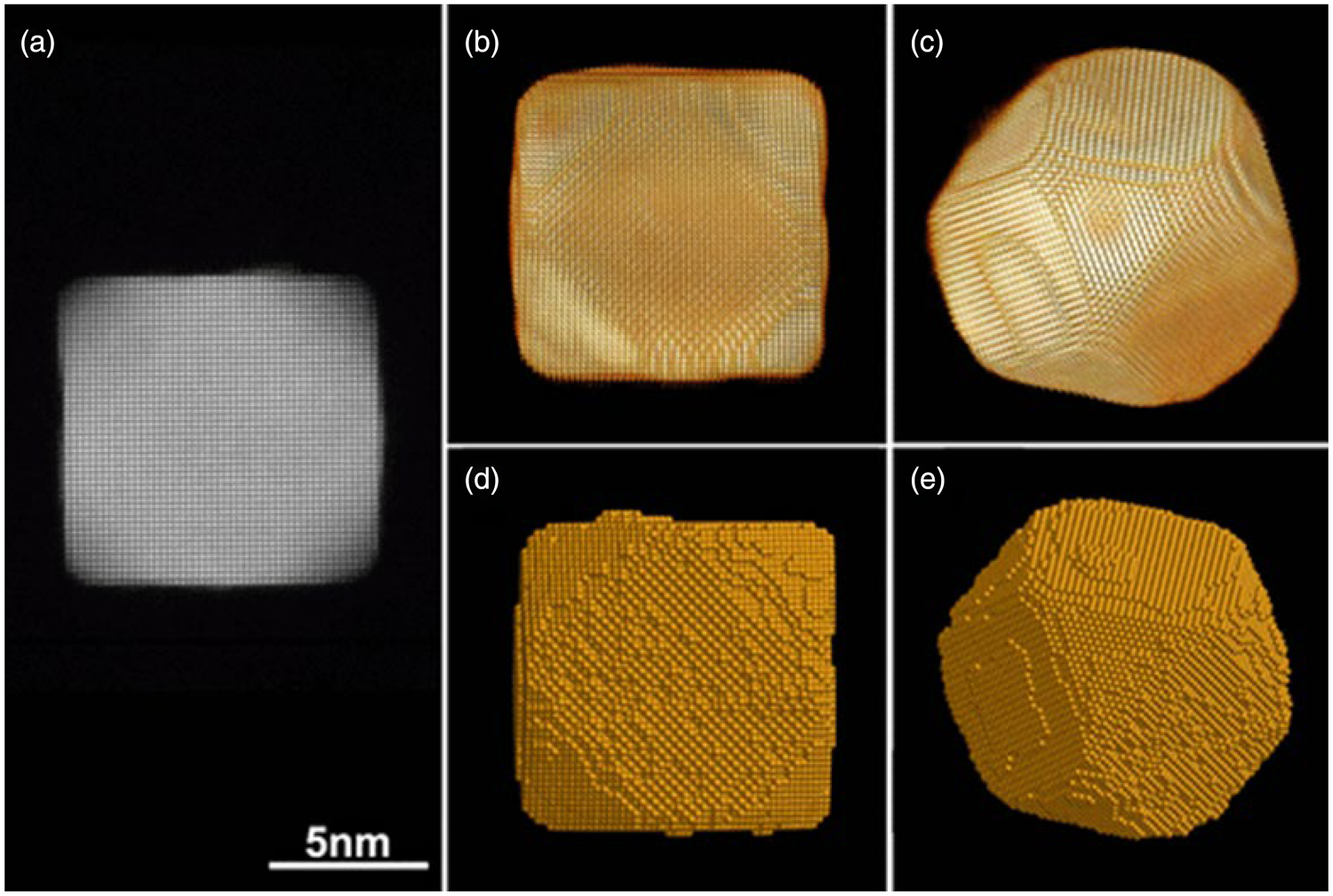
Fig. 21. Comparison of the 3D shapes obtained by the reconstruction of a high-resolution tomography series and by atom-counting, for the same Pt NP. (a) High-resolution HAADF STEM image of a Pt NP which was used for conventional high-resolution electron tomography and for atom-counting and relaxation. (b,c) Three-dimensional visualization of the reconstructed volume obtained by conventional high-resolution tomography, along different viewing directions. (d,e) Three-dimensional models of the same Pt NP obtained by using atom-counting and relaxation. Reproduced from Altantzis et al. (Reference Altantzis, Lobato, De Backer, Béché, Zhang, Basak, Porcu, Xu, Sánchez-Iglesias, Liz-Marzán, Van Tendeloo, Van Aert and Bals2019).
The atom-counting method discussed above was applied to investigating hetero-atom nanostructures by extending the above method to the atomic lensing model (van den Bos et al., Reference van den Bos, De Backer, Martinez, Winckelmans, Bals, Nellist and Van Aert2016, Reference van den Bos, Janssens, De Backer, Nellist and Van Aert2019). This new approach allows an identification of scattering cross-section of mixed columns that possess 3D arrangements of different atoms. By taking nonlinear scattering cross-sections into account, via the assumption that dynamical diffraction effects could be considered as a superposition of individual atomic focusers, the authors demonstrated that the lensing effect of an atom was independent of defocus. Through such model-based calculations, intensities of columns of mixed atoms would be predicted, leading to differentiation of atomic columns with different degrees of atom mixing. The combination of the statistical parameter estimation with model-order selection proved to be useful for establishing maximum a posteriori (MAP) probability rule (Fatermans et al., Reference Fatermans, den Dekker, Müller-Caspary, Lobato, O'Leary, Nellist and Van Aert2018, Reference Fatermans, Van Aert and den Dekker2019) which would allow structural determination of unknown structures in an automatic and objective manner and determination of atomic columns with high reliability and single-atom sensitivity. The MAP rule was extended to simultaneously acquired ABF and ADF images, enabling structural determination of both light and heavy elements in a crystalline sample (Fatermans et al., Reference Fatermans, den Dekker, Müller-Caspary, Gauquelin, Verbeeck and Van Aert2020). It is expected that such modeling processes are not limited to ADF and ABF detector configurations but may be extended to model-based analysis of all STEM imaging modes including 4D-STEM.
Atomic-Resolution Three-Dimensional Imaging and Elemental Mapping
Atomic-Resolution Electron Tomography
Understanding material properties and functionalities at the most fundamental level requires precise measurement of 3D positions of atoms with picometer or sub-picometer precision. Practical materials often contain surfaces/interfaces, defects, and/or nanoscale heterogeneities which can strongly influence their properties and performance. The 2D projection images that we discussed above do not fully represent the underlying 3D structures and can lead to significant errors in assessing the true 3D structures of the specimen of interest. The tomographic approach is used for revealing hidden structures that are not directly accessible by 2D projection images. Radon mathematically worked out how to project a high-dimension object into a lower-dimension space (Radon, Reference Radon1917). The inverse function of the Radon transform provides the mathematical foundation of tomographic techniques. Electron tomography, developed in the late 1960s (De Rosier & Klug, Reference De Rosier and Klug1968), was successfully applied to imaging 3D structures of biological specimens at cryogenic temperatures (Unwin & Henderson, Reference Unwin and Henderson1975; Dubochet et al., Reference Dubochet, Adrian, Chang, Homo, Lepault, McDowall and Schultz1988). The method developed for biological specimens, however, may not be directly applicable for materials science applications. In biological and noncrystalline inorganic systems, the use of BF TEM imaging is appropriate because the mass-thickness contrast satisfies the “projection requirement” that the recorded signal should be a monotonic function of some physical property (Hawkes, Reference Hawkes and Frank1992). If this requirement is not satisfied, then 3D reconstruction becomes too complicated and conventional real-space, back-projection method may not be approachable. For investigation of crystalline materials, the presence of diffraction contrast and Fresnel fringes in TEM images fails the projection requirement and can lead to serious artifacts in 3D reconstructions. The unique characteristics of the HAADF-STEM signal are, however, appropriate for tomographic imaging of crystalline materials provided that electron-beam-induced effects are alleviated or eliminated. The early development and applications of electron tomography in materials science have been reviewed (Midgley & Weyland, Reference Midgley and Weyland2003; Midgley & Dunin-Borkowski, Reference Midgley and Dunin-Borkowski2009).
Since incoherent ADF STEM imaging substantially suppresses the diffraction and phase contrast of crystalline regions of the sample and yields atomic number sensitivity with sub-Ångstrom spatial resolution, this imaging mode is particularly suited for achieving atomic-resolution tomography (Miao et al., Reference Miao, Ercius and Billinge2016) (Fig. 22). The missing wedge problem can be overcome by using needle-shaped specimens, allowing a 360° rotation around the needle axis (Xu et al., Reference Xu, Chen, Wu, Scott, Theis, Ophus, Bartels, Yang, Ramezani-Dakhel, Sawaya, Heinz, Marks, Ercius and Miao2015). Another problem in STEM tomography is electron-beam-induced effects on the specimen. Since many images of the same specimen region are required for atomic-resolution STEM tomography, electron-beam-induced damage to the specimen may become a major issue, especially for studies of electron-beam-sensitive materials. Appropriate electron energies need to be selected to reduce knock-on damage (Egerton et al., Reference Egerton, Li and Malac2004, Reference Egerton, McLeod, Wang and Malac2010). A dose-efficient STEM approach (Ophus et al., Reference Ophus, Ciston, Pierce, Harvey, Chess, McMorran, Czarnik, Rose and Ercius2016b), employment of direct electron detectors (McMullan et al., Reference McMullan, Faruqi, Clare and Henderson2014; Tate et al., Reference Tate, Purohit, Chamberlain, Nguyen, Hovden, Chang, Deb, Turgut, Heron, Schlom, Ralph, Fuchs, Shanks, Philipp, Muller and Gruner2016), and low-exposure acquisition scheme (Scott et al., Reference Scott, Chen, Mecklenburg, Zhu, Xu, Ercius, Dahmen, Regan and Miao2012; Chen et al., Reference Chen, Zhu, White, Chiu, Scott, Regan, Marks, Huang and Miao2013) all help alleviate electron-beam-induced effects. As discussed in the section “Correction of image distortions and structural measurement with picometer precision,” various types of image distortions in each ADF STEM image of a tilt series should be corrected by the corresponding approaches and robust reconstruction algorithms should be used. Since as low dose of electrons as possible is highly desired to alleviate electron-beam effects, de-noising algorithms were developed and applied to improving image quality (Dabov et al., Reference Dabov, Foi, Katkovnik and Egiazarian2007). The center-of-mass method was applied to aligning tilt series of STEM imaging stacks (Scott et al., Reference Scott, Chen, Mecklenburg, Zhu, Xu, Ercius, Dahmen, Regan and Miao2012). To achieve higher precision in defining atom positions, iterative refinement in image alignment should be implemented by initially computing a 3D reconstruction from the coarse-aligned tilt series. Then, the back-projected 2D image series, obtained from the initially reconstructed 3D image, are compared with the corresponding experimental 2D images of the same tilt angles to check for consistence. Quantitative comparison of the calculated and measured images and iterative algorithms allow fine-tuning of the reconstructed 3D image so that all the projected images match the experimental data.
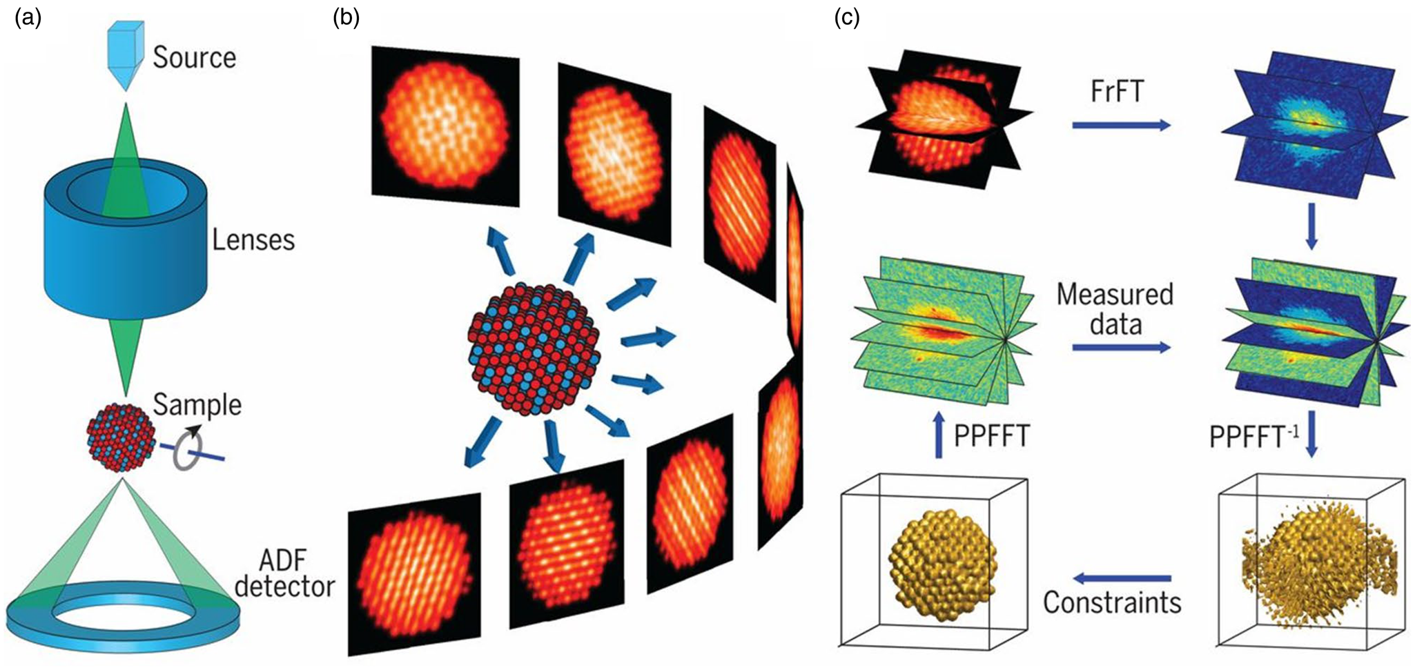
Fig. 22. Schematic illustration of an atomic-resolution electron tomography experiment. (a) An electron beam is focused on a small spot and scanned over a sample to form a 2D ADF image. (b) By rotating the sample around a tilt axis, a series of 2D ADF images is recorded at different tilt angles. (c) After preprocessing and alignment, the tilt series image dataset is inverted to Fourier slices by fractional Fourier transform (FrFT). A 3D reconstruction is computed by using an iterative algorithm based on pseudopopular fast Fourier (PPFFT). From the 3D reconstruction, the coordinates of individual atoms are traced and refined to produce the 3D atomic model of the specimen. Reproduced from Miao et al. (Reference Miao, Ercius and Billinge2016).
In addition to establishing robust experimental protocols for atomic-resolution tomography, iterative tomographic reconstruction algorithms play the most critical role in achieving the desired 3D precision measurement. Real-space iterative algorithms compute a 3D reconstruction by iteratively solving a system of linear equations, in which positivity and mathematical regularization can be incorporated as constraints to reduce artifacts (Gordon et al., Reference Gordon, Bender and Herman1970; Gilbert, Reference Gilbert1972; Andersen & Kak, Reference Andersen and Kak1984). The hybrid space algorithms rely on iterations between real and Fourier space. From an aligned tilt series, each image is inverted to a Fourier representation by fractional Fourier transform (Bailey & Swarztrauber, Reference Bailey and Swarztrauber1991). Detailed descriptions of the reconstruction algorithm with equal-slope tomography were described by Mao et al. (Reference Mao, Fahimian, Osher and Miao2010). Quantitative comparison with experimental data suggested that the equal-slope approach produced 3D reconstructions with higher resolution, better image contrast, and less distortion than real-space iterative algorithms. This approach, however, requires that the experimental tilt angles must be consistent with equal-slope increments (Miao et al., Reference Miao, Förster and Levi2005).
By fitting atoms rigidly onto a crystal lattice, discrete tomography was developed to image the 3D atomic structure of a metal nanoparticle (Van Aert et al., Reference Van Aert, Batenburg, Rossel, Erni and Van Tendeloo2011). Compressed sensing technique was applied to electron tomography with the expectation to significantly reduce electron-beam-induced effects and image distortions by sparse sampling (Leary et al., Reference Leary, Saghi, Midgley and Holland2013). The compressed sensing electron tomography method was successfully applied to imaging localized surface plasmon resonances of a silver nanocube, providing atomic-scale information (Nicoletti et al., Reference Nicoletti, de la Peña, Leary, Holland, Ducati and Midgley2013). A design of sparse sampling domains and choice of adjustable parameters may prove challenging for noisy images (Leary et al., Reference Leary, Saghi, Midgley and Holland2013).
The atomic-resolution tomography technique proved to be valuable for determining 3D structures of metal nanoparticles. Volume and iso-surface renderings of the 3D reconstruction of an Au nanoparticle showed the coordinates of individual surface atoms as well as the internal structures of the multiply-twinned Au icosahedral nanoparticle (Scott et al., Reference Scott, Chen, Mecklenburg, Zhu, Xu, Ercius, Dahmen, Regan and Miao2012). In studying crystal defects in metal nanoparticles, Chen et al. (Reference Chen, Zhu, White, Chiu, Scott, Regan, Marks, Huang and Miao2013) investigated the internal 3D structure of Pt nanoparticles, revealing 3D atomic arrangements of screw dislocations and atomic steps at Pt twin boundaries. They further deduced that a strain relaxation mechanism was associated with multiply-twinned Pt decahedral nanoparticles. Such insights into the formation of crystal defects might not be extracted from conventional 2D projection images. By using a tungsten needle sample, Xu et al. (Reference Xu, Chen, Wu, Scott, Theis, Ophus, Bartels, Yang, Ramezani-Dakhel, Sawaya, Heinz, Marks, Ercius and Miao2015) conducted 3D measurements of individual atom coordinates, atomic displacements, and strain tensor parameters. By selecting nonchanneling conditions to minimize electron dynamical scattering effects and by measuring many images at various sample orientations, the authors were able to determine the coordinates of 3,769 individual atoms of the tungsten needle with a precision of about 10.5, 15, and 5.5 pm along the x-, y-, and z-axis, respectively. Such an approach enables 3D identification and localization of point defects in materials with high precision and without any prior knowledge. By comparing the coordinates of individual atoms with a model tungsten crystal lattice, the atomic displacement field and the strain tensor of the tungsten needle were determined. The ability of precisely determining 3D positions of individual atoms of nanostructures opens the door toward directly investigating the properties and functionalities of a plethora of nanoscale structures, systems, or devices.
Many nanostructures contain different types of elements, for example, bimetallic or multi-metallic alloy nanoparticles. Correlating the 3D atomic arrangements of chemical order/disorder and crystal defects with material properties becomes critical for designing nanostructured functional materials, especially when the structural data are combined with first-principles calculations. Yang et al. (Reference Yang, Chen, Scott, Ophus, Xu, Pryor, Wu, Sun, Theis, Zhou, Eisenbach, Kent, Sabirianov, Zeng, Ercius and Miao2017b) determined the 3D coordinates of 6,569 iron and 16,627 platinum atoms in an iron–platinum nanoparticle, and correlated the chemical order/disorder and crystal defects with material properties at the single-atom level. They identified atomic composition, grain boundaries, anti-phase boundaries, anti-site point defects, and swap defects in 3D with a precision of ~20 pm. By using such structural and compositional information as direct input for DFT calculations, the authors were able to determine material properties such as atomic spin and orbital magnetic moments and local magneto-crystalline anisotropy, significantly advancing the fundamental understanding of structure–property relationships.
In polycrystalline materials, especially nanocrystalline materials, grain boundary (GB) structures and chemistry often play the most important role in determining materials properties. Design and engineering of GBs offer a route to developing nanostructured materials with novel properties. Atomic-resolution electron tomography proved to be valuable for extracting 3D atomic coordinates of general high-angle GBs (Wang et al., Reference Wang, Duan, Chen, Wu, Qi, Ye, Jin, Xin and Du2020). With atomic-resolution 3D imaging, the authors found that high-angle GBs completely lose translational symmetry due to undulated curvature related to the configurations of the structural units. Kinks and jogs at single-atom scale in dislocation-type GBs and their mobility were directly visualized in 3D at atomic resolution. Such understanding of GBs may bring deep insights into the understanding of GB behavior and in developing new material systems with desirable properties that are controlled by specific types of GBs.
Experimental investigation of dynamic events such as nucleation of clusters/nanoparticles or melting of nanocrystals faces significant challenges, especially when atomic-resolution 3D imaging of such dynamic events is required. By using an identical location STEM approach, Zhou et al. (Reference Zhou, Yang, Yang, Kim, Yuan, Tian, Ophus, Sun, Schmid, Nathanson, Heinz, An, Zeng, Ercius and Miao2019) were able to evaluate nucleation processes of FePt nanoparticles in 3D. They captured the atomic-scale structure and dynamics of the same nuclei undergoing growth, fluctuation, dissolution, merging, and/or division, all of which are regulated by the order parameter distribution and its gradient. They further discovered that the early-stage nucleation process might not follow the classical nucleation theory. It is expected that with further improvement in methodology atomic-resolution 3D imaging with time resolution will provide new routes to understanding the fundamentals of phase transition, atomic diffusion, grain boundary dynamics, interface motion, defect dynamics, and surface reconstructions of nanoscale structures and systems. The atomic-resolution tomography method proved to be extremely powerful for studying 2D nanostructures with the goal of correlating their electronic, optical and chemical properties to 3D atomic positions of various elements and/or defects such as dopants and vacancies. Tian et al. (Reference Tian, Kim, Yang, Ciccarino, Gong, Yang, Yang, Duschatko, Yuan, Ajayan, Idrobo, Narang and Miao2020) determined the 3D atomic positions of Re-doped MoS2 with a precision of ~4 pm. They measured the 3D bond distortion and local strain tensor, caused by the presence of dopant atoms. By using such 3D atomic coordinates of all the entities in the specimen as input for DFT calculations, the authors claimed to obtain more accurate electronic band structures, confirming direct correlation of 3D atomic structure to electronic properties.
As discussed in the section “Nanodiffraction, Ronchigram, ptychography, and 4D-STEM,” electron ptychography efficiently utilizes scattered electrons to construct ultrahigh-resolution images and enables low-dose STEM imaging with sub-Ångstrom resolution. Atomic electron tomography, on the other hand, permits 3D imaging but requires relatively longer time of electron-beam irradiation of the specimen region of interest. Therefore, the combination of ultrahigh-resolution electron ptychography with atomic electron tomography may provide an effective approach to low-dose 3D imaging of both light and heavy elements in a crystalline specimen. Chang et al. (Reference Chang, Kim, Rana, Tian, Zhou, Ercius and Miao2020) applied this approach to the study of ZnO nanoparticles and WS2/WSe2 heterostructures. Since electron ptychography already requires 4D datasets and atomic electron tomography requires a series of tilt images, the data analysis algorithm becomes extremely critical to such experiments. The authors, however, determined the 3D atomic coordinates of individual zinc and oxygen atoms as well as defects within the ZnO nanoparticles. By comparing with image simulations, the authors resolved every layer, including the lightest sulfur layer, of the vertical WS2/WSe2 van der Waals heterostructure with atomic resolution. It is expected that with faster computers and robust reconstruction algorithms the ptychography-based atomic electron tomography may become a routinely accessible method for determining precise 3D atomic structures of radiation-sensitive systems and a plethora of practical materials such as catalysts, functional oxides, and glasses.
Atomic-Resolution STEM Depth Sectioning
Optical-sectioning microscopy, for example, achieved on a laser scanning confocal microscope, is a powerful technique for visualizing 3D structures of biological systems (Conchello & Lichtman, Reference Conchello and Lichtman2005). With the use of a large probe-forming aperture to form a sub-Ångstrom probe in an ac-STEM, the depth of field (DOF) should be significantly reduced, enabling depth sectioning meaningful by recording a series of images at different defocus values. In principle, similar to optical-sectioning microscopy, 3D images would be reconstructed from such a series of 2D projection images. A significant difference from confocal optical microscopy is that STEM imaging does not use a collection pin-hole, leading to degradation of depth sensitivity. Compared with tomography, the optical-sectioning process does not require specimen tilt, drastically reducing experimental complexity. This STEM sectioning technique, however, had not been frequently used prior to the ready availability of atomic-resolution Z-contrast imaging. The detection of individual Sb-dopant atoms within a crystalline Si by ADF STEM imaging (Voyles et al., Reference Voyles, Muller, Grazul, Citrin and Gossmann2002) invited the question on 3D localization of individual dopant atoms by a direct imaging technique. van Benthem et al. (Reference van Benthem, Lupini, Kim, Baik, Doh, Lee, Oxley, Findlay, Allen, Luck and Pennycook2005) evaluated the optical-sectioning method with ADF signal (with a probe size of ~0.1 nm) to localize individual Hf atoms within an SiO2 passivating layer of an HfO2/SiO2/Si alternative gate dielectric stack. By acquiring a through-focal series of images, the 3D locations of dopant atoms within a crystal were realized with a lateral resolution <0.1 nm and a depth resolution of ~0.5 nm. The authors concluded that the through-focal series method was sensitive to detecting individual dopant/impurity atoms and proposed that the depth sectioning method would be applicable to spectroscopy experiments as well.
Borisevich et al. (Reference Borisevich, Lupini and Pennycook2006) provided an evaluation of STEM depth sectioning approach, examined the resolution and contrast parameters, and demonstrated how 3D datasets could be collected and analyzed for several test systems including supported metal catalysts. The authors were able to localize nanometer-size particles and even single atoms. They conducted statistical analysis of the acquired dataset and quantified the effective focal depth, controlled by the size of the probe-forming aperture, sample parameters, signal-to-noise ratio, and image acquisition settings. By using a highly convergent electron probe, Ruben et al. (Reference Ruben, Cosgriff, D'Alfonso, Findlay, LeBeau and Allen2012) investigated the depth-related features of layered heterostructures. The authors fixed the electron probe at an atomic column and monitored the variations in ADF signal strength with probe defocus. The authors were able to identify intensity peaks that were related to the heterojunctions and crystal surfaces, leading to an estimate of sample thickness and heterojunction locations. Channeling of incident electrons along atomic columns plays an important role, leading to reduced depth resolution. These authors demonstrated localization of crystal-vacuum surfaces to within 1 nm and buried interfaces to within 2 nm. Ishikawa et al. (Reference Ishikawa, Lupini, Hinuma and Pennycook2015) theoretically evaluated imaging of top/subsurface atomic structures and were able to identify depth location of single dopants, single vacancies, and other types of point defects by large-angle illumination STEM imaging. They proposed a method to measure specimen properties such as thickness or three-dimensional surface morphology using observations from a single crystallographic orientation. Imaging atomic displacements in screw dislocations are challenging because the associated atoms are predominantly displaced parallel to the dislocation line; screw displacements are parallel to the electron beam and become invisible when viewed end-on. By using the ADF sectioning approach, Yang et al. (Reference Yang, Lozano, Pennycook, Jones, Hirsch and Nellist2015) directly imaged screw displacements with the dislocation lying in a plane transverse to the electron beam. The authors reported direct imaging of a screw dissociation with a 1.65-nm dissociation distance in GaN, demonstrating an alternative approach to characterizing dislocation core structures.
Xin & Muller (Reference Xin and Muller2009) investigated the contrast transfer function of the ADF depth sectioning approach and found a missing-cone problem, similar to that of tilt-series tomography. They worked out the dependence of the elongation on the probe-forming convergence angle. The large elongation factor along the incident beam direction results in highly distorted shapes of 3D objects and unexpected artifacts due to loss of information. The authors further experimentally investigated the elongation effect and the missing-cone problem in real and reciprocal space. The performance limits of different S/TEM-based imaging modes were compared. Nellist (Reference Nellist2017) discussed the contrast transfer function for 3D imaging, investigated the elongation factor, and concluded that, although sub-Ångstrom-scale lateral resolution could be achievable, the vertical probe size would be too large for differentiating individual atoms in a nanostructure. By combining depth-sectioning and precise atom-counting methods, Alania et al. (Reference Alania, Altantzis, De Backer, Lobato, Bals and Van Aert2017) reconstructed 3D atomic-resolution images of Au nanorods. Although the depth resolution was not good enough to allow precise determination of each atom within a column of atoms, this approach provided depth location of an entire atomic column as a whole, enabling 3D determination of the morphology of the nanostructure of interest. Significant challenges, however, remain to be overcome before 3D atomic-resolution imaging by optical depth sectioning can be realized in STEM.
Atomic-Resolution Elemental Mapping
Atomic-Resolution Chemical Mapping by EELS
Ever since the invention of the field-emission STEM by Crewe, EELS has played a major role in identifying composition or valence state of the probed region of interest with a spatial resolution determined by the electron probe size and an impact parameter (Ritchie & Howie, Reference Ritchie and Howie1988; Colliex et al., Reference Colliex, Imhoff, Perez-Omil, Stéphan, Suenaga and Tence1999; García de Abajo, Reference García de Abajo2010). For core-loss edges, their shapes in EELS spectra reflect the underlying local partial density of states modified by the presence of a core hole (Colliex & Jouffrey, Reference Colliex and Jouffrey1972). Such core-loss peaks not only carry element specific information but also the valence state or bonding of the probed atom or columns of atoms. Batson, using an improved HB501 STEM and a high-resolution electron spectrometer (Batson, Reference Batson1986, Reference Batson1988, Reference Batson1993), resolved the different bonding states of silicon atoms (Si0, Si2+, Si4+) across an Si–SiO2 interface and the oxidation state of individual columns of unit cells, containing pairs of silicon atoms, firmly establishing STEM-EELS as a powerful tool for atomic-scale analysis of materials chemistry. By using an electron probe size of ~0.22 nm and a thin specimen, Browning et al. (Reference Browning, Chisholm and Pennycook1993), with the assistance of ADF STEM imaging to identify the atomic positions of an epitaxial CoSi2–Si interface, demonstrated that an EELS signal could be used to obtain information about chemical composition at atomic-scale resolution. Browning et al. (Reference Browning, Chisholm and Pennycook1993) proposed the possibility of interpreting the observed fine structure of the EELS spectra in terms of chemical bonding on the atomic scale. Almost at the same time, Muller et al. (Reference Muller, Tzou, Raj and Silcox1993) reported spatial mapping of carbon sp 2 and sp 3 states with a subnanometer spatial resolution, clearly demonstrating the feasibility of 2D mapping of bonding states at buried interfaces with an image resolution approaching atomic level.
The detection limit of the EELS technique was predicted to be a single atom (Isaacson & Johnson, Reference Isaacson and Johnson1975). With the use of a modified Gatan PEELS 666 on a non-aberration-corrected VG HB501, Suenaga et al. (Reference Suenaga, Tence, Mory, Colliex, Kato, Okazaki, Shinohara, Hirahara, Bandow and Iijima2000) not only analyzed Gd atoms inside a single chain of metallofullerene molecules (Gd@C82), which were encapsulated within a single-wall carbon nanotube, but also formed elemental maps of individual single Gd atoms. The carbon nanotubes facilitated stabilization of the Gd-containing molecular complexes, significantly alleviating electron-beam-induced effects. Even though the isolated Gd atoms were detected and spatially resolved, the spatial resolution was only ~0.6 nm but sufficient to resolve the widely spaced Gd atoms. By using an ac-STEM to significantly increase the intensity within a sub-Ångstrom electron probe, Varela et al. (Reference Varela, Findlay, Lupini, Christen, Borisevich, Dellby, Krivanek, Nellist, Oxley, Allen and Pennycook2004) were able to conduct spectroscopic imaging of single atoms embedded within a bulk solid. Dynamical simulations confirmed that the spectroscopic information was spatially confined to the La atom within the CaTiO3. The authors demonstrated the potential of locating the depth of La-dopant atoms within the crystal. Atomic-resolution EELS analysis and mapping on a single-atom level are now routinely available on ac-STEM instruments, opening up new opportunities for studying a variety of materials systems with single-atom chemical sensitivity (Suenaga et al., Reference Suenaga, Sato, Liu, Kataura, Okazaki, Kimoto, Sawada, Sasaki, Omoto, Tomita, Kaneyama and Kondo2009; Suenaga & Koshino, Reference Suenaga and Koshino2010; Ramasse et al., Reference Ramasse, Seabourne, Kepaptsoglou, Zan, Bangert and Scott2012; Zhou et al., Reference Zhou, Kapetanakis, Prange, Pantelides, Pennycook and Idrobo2012a, Reference Zhou, Oxley, Lupini, Krivanek, Pennycook and Idrobo2012b; Lin et al., Reference Lin, Teng, Chiu and Suenaga2015). Electron-beam-induced effects, however, pose major limitations on the chemical and structural integrity of the specimen of interest. For example, metal adatoms on catalyst supports may not maintain their chemical environment under the conditions for single-atom STEM-EELS analysis.
Atomic-resolution chemical mapping of columns of elements require small probe sizes since the distances among the neighboring columns of atoms are usually <0.3 nm. The availability of an ac-STEM, which allows a large probe-forming aperture to produce a sub-Ångstrom electron probe with a significantly increased beam current (Batson et al., Reference Batson, Dellby and Krivanek2002), made it possible to obtain atomic-resolution EELS line profiles of Ti L-shell EELS in a SrTiO3 crystal (Allen et al., Reference Allen, Findlay, Lupini, Oxley and Pennycook2003). Even with a non-aberration-corrected VG HB501 dedicated STEM, Bosman et al. (Reference Bosman, Keast, García-Muñoz, D'Alfonso, Findlay and Allen2007) were able to demonstrate the plausibility of 2D atomic-resolution chemical mapping of Bi0.5Sr0.5MnO3 by using a probe-forming semi-angle and EEL detector semi-angle of ~24 mrad and a mapping acquisition time of ~10 min. With the use of an ac-STEM and stable environment/microscope, Kimoto et al. (Reference Kimoto, Asaka, Nagai, Saito, Matsui and Ishizuka2007) demonstrated 2D atomic-column imaging of a crystal specimen using localized inelastically scattered electrons. The atomic columns of La, Mn, and O in the layered manganite La1.2Sr1.8Mn2O7 were clearly visualized. These authors further investigated the dependence of delocalization on the energy of inelastically excited primary electrons. Oxley et al. (Reference Oxley, Varela, Pennycook, van Benthem, Findlay, D'Alfonso, Allen and Pennycook2007) theoretically investigated the origin of the atomic-resolution EELS signal and discovered that delocalization of inelastically scattered electrons would not preclude atomic-resolution but would reduce image contrast. They further discussed the appearance and origins of volcano-like features at the EELS edge peaks.
A 2D EELS chemical map that contains bonding information requires much higher beam current to significantly improve the signal-to-noise ratio. By using a Nion STEM with fifth-order correction (Krivanek et al., Reference Krivanek, Corbin, Dellby, Elston, Keyse, Murfitt, Own, Szilagyi and Woodruff2008) to further focus more electrons into a finer electron probe and a modified spectrometer (Krivanek et al., Reference Krivanek, Corbin, Dellby, Elston, Keyse, Murfitt, Own, Szilagyi and Woodruff2008) to extend EELS collection angles up to ~60 mrad, Muller et al. (Reference Muller, Kourkoutis, Murfitt, Song, Hwang, Silcox, Dellby and Krivanek2008) were able to obtain impressive atomic-resolution chemical bonding maps of a La0.7Sr0.3MnO3/SrTiO3 multilayer sample. Changes in the titanium bonding due to variations in the local environment helped distinguish chemical interdiffusion from imaging artifacts. The success of this work, because of the improved optics to significantly increase both the probe convergence and EELS collection angles, unambiguously proves that 2D chemical imaging at the atomic scale with simultaneous elemental identification and visualization of local bonding states can be readily achieved. Muller (Reference Muller2009) summarized the achievements in atomic-resolution 2D elemental and bonding mapping and assessed that there could be over a 100-fold difference between corrected and conventional STEM instruments in terms of probe current or spectrum acquisition speed. Further improvement in detector and detection configuration as well as the electron source could facilitate a significant increase in the collected EELS signals. Electron-beam-induced effects, however, may set the limit for useful electron probe currents and low-voltage approach might alleviate some of the electron-beam-induced effects. Wang et al. (Reference Wang, Saito, McKenna, Gu, Tsukimoto, Shluger and Ikuhara2011) conducted atomic-scale chemical analysis of grain boundaries in polycrystalline materials and revealed the interplay between atomic defects and impurities at the grain boundaries. Through such investigations, one can gain deep insights in understanding grain boundary transformations and how they modify material properties. Applications of atomic-resolution chemical mapping to various material systems have greatly enhanced our understanding of the atomic-world of materials (Browning et al., Reference Browning, Arslan, Ito, James, Klie, Moeck, Topuria and Xin2001; Kourkoutis et al., Reference Kourkoutis, Xin, Higuchi, Hotta, Lee, Hikita, Schlom, Hwang and Muller2010; Trasobares et al., Reference Trasobares, López-Haro, Kociak, March, de La Peña, Perez-Omil, Calvino, Lugg, D'Alfonso, Allen and Colliex2011; Ishikawa et al., Reference Ishikawa, Lupini, Findlay, Taniguchi and Pennycook2014; Zamani et al., Reference Zamani, Hage, Lehmann, Ramasse and Dick2018). Figure 23 shows a large-area atomic-resolution EELS map of oxide superlattices. Such atomic-resolution elemental maps aid the fundamental understanding of quantum many-body interactions (Monkman et al., Reference Monkman, Adamo, Mundy, Shai, Harter, Shen, Burganov, Muller, Schlom and Shen2012).
Fig. 23. EELS map over a wide field of view from an n = 3 (LaMnO3)2n/(SrMnO3)n/SrTiO3 film measured, showing La in green, Mn in red, and Ti in blue. The irregularity of the topmost surface in this image is an artifact of the preparation procedure for EELS and HAADF-STEM measurements and does not reflect the topmost surface of the as-grown film. Adapted from Monkman et al. (Reference Monkman, Adamo, Mundy, Shai, Harter, Shen, Burganov, Muller, Schlom and Shen2012).
Watanabe et al. (Reference Watanabe, Kanno and Okunishi2010) discussed practical aspects of acquiring atomic-resolution 2D chemical maps by collecting either EELS or X-ray energy-dispersive spectrometry (XEDS) signals. In addition to discussing forming appropriate probe sizes/currents, these authors emphasized the development of sophisticated approaches to data acquisition and analysis and provided examples of atomic-resolution chemical mapping of different types of materials. Cueva et al. (Reference Cueva, Hovden, Mundy, Xin and Muller2012) discussed the importance of improving background estimation and increasing chemical sensitivity in atomic-resolution chemical maps by utilizing new algorithms to analyze dose-limited spectral maps. They proposed an analysis procedure by considering a linear combination of power laws and local background averaging. They identified potential issues with the principal component analysis approach and discussed alternative approaches to processing chemical maps. Localization/delocalization of inelastic electron scattering events, EELS signal strength, and the effects of elastic/diffuse scattering on the collected EELS signal were extensively investigated to understand the nature of atomic-resolution elemental maps (Dwyer, Reference Dwyer2013; Lugg et al., Reference Lugg, Neish, Findlay and Allen2014; Allen, Reference Allen2017).
Atomic-Resolution Chemical Mapping by XEDS
Atomic-resolution elemental mapping via XEDS was accomplished in 2010 (Chu et al., Reference Chu, Liou, Chang, Choa and Chen2010; D'Alfonso et al., Reference D'Alfonso, Freitag, Klenov and Allen2010; Watanabe et al., Reference Watanabe, Kanno and Okunishi2010) and was applied to qualitative study of various material systems (Klenov & Zide, Reference Klenov and Zide2011; Allen et al., Reference Allen, D'Alfonso, Freitag and Klenov2012; Kotula et al., Reference Kotula, Klenov and Von Harrach2012; Itakura et al., Reference Itakura, Watanabe, Nishida, Daio and Matsumura2013; Lu et al., Reference Lu, Xiong, Van Benthem and Jia2013). A qualitative interpretation of atomic-resolution XEDS maps seems intuitive but quantitative analysis requires consideration of the effects of strong dynamical scattering (channeling) of the electron probe on the generation of XEDS signals. When a crystal is aligned with a zone-axis parallel to the incident beam direction (i.e., the condition for atomic-resolution imaging), the electron beam becomes localized around the columns of nuclei, generating X-ray signals. In this case, however, the relationship between the concentration of a particular element and the detected X-ray signal strength is generally nonlinear, significantly complicating the quantification of atomic-resolution XEDS maps. Forbes et al. (Reference Forbes, D'Alfonso, Williams, Srinivasan, Fraser, McComb, Freitag, Klenov and Allen2012) investigated the contribution of thermally scattered electrons to the collected XEDS signal. Although the experimental results could not be directly interpretable, they demonstrated that first-principle simulations would be useful for understanding the intensity of atomic-resolution XEDS maps. Kothleitner et al. (Reference Kothleitner, Neish, Lugg, Findlay, Grogger, Hofer and Allen2014) showed good quantitative agreement between experimental XEDS maps and electron-channeling-based simulations when they evaluated the relative signal strengths of different atomic columns. However, due to electron-channeling effects, the measured compositions might not represent the true stoichiometry of the probed region. The consequences of electron channeling include (1) changes in relative image contrast and (2) changes in absolute-scale intensity. Chen et al. (Reference Chen, D'Alfonso, Weyland, Taplin, Findlay and Allen2015), using an atomic-scale electron probe and first-principle simulations, demonstrated good agreement between experiment and simulation in the total number of X-ray counts recorded for atomic-resolution maps of an SrTiO3 specimen.
The use of multiple, large-area, silicon-drift detectors (SDDs) in an ac-STEM (Lu et al., Reference Lu, Xiong, Van Benthem and Jia2013) enables a sufficient signal-to-noise ratio to produce high-quality atomic-resolution XEDS maps. The increased complexity of such detector geometries requires accurate numerical modeling to determine the effective detector solid-angle and X-ray absorption within the specimen and from the sample holder. Since electron-channeling effects could become significant in quantitative analysis of atomic-resolution XEDS maps, Dycus et al. (Reference Dycus, Xu, Sang, D'Alfonso, Chen, Weyland, Allen, Findlay and LeBeau2016) investigated the influence of key experimental parameters on such XEDS maps. They studied the role of the probe-forming convergence semi-angle, sample thickness, lattice spacing, and dwell/collection time in determining the strength of the acquired XEDS signals. These authors found that an optimum specimen-dependent probe-forming convergence angle exists for maximizing the signal-to-noise ratio of atomically resolved XEDS maps. These practical considerations provided deeper insights into the selection of experimental parameters to acquire better, and to correctly interpret, atomic-resolution XEDS maps.
Even with multiple SDDs and aberration-corrected electron probes, the XEDS signal is still relatively weak when the specimen is very thin (e.g., 2D materials). For thicker specimens, both beam broadening and dynamic scattering effects can severely degrade image resolution and complicate quantitative interpretation of atomic-resolution XEDS maps. For each sample, there seems to exist a range of specimen thicknesses that give both a reasonable signal-to-noise ratio and a tolerable simple analysis of atoms column-by-column. A quantitative interpretation of atomic-resolution XEDS maps, however, require detailed simulations (Lugg et al., Reference Lugg, Kothleitner, Shibata and Ikuhara2015b; Chen et al., Reference Chen, Weyland, Sang, Xu, Dycus, LeBeau, D'Alfonso, Allen and Findlay2016; MacArthur et al., Reference MacArthur, Brown, Findlay and Allen2017). Lu et al. (Reference Lu, Moya, Yuan and Zuo2018) used a single-frame scanning technique rather than an averaging multiple-frame approach to avoid peak broadening (Fig. 24). They showed that the localization of emitted X-rays to the atomic columns strongly depended on crystal thickness. They suggested the use of a thin crystal to improve spatial resolution in atomic-scale XEDS mapping. The quantitative analysis of atomic-resolution XEDS maps of interfaces is challenging and more complex because electrons may channel differently in different crystalline specimens (Spurgeon et al., Reference Spurgeon, Du and Chambers2017; Feng et al., Reference Feng, Lugg, Kumamoto, Shibata and Ikuhara2018). By slightly tilting the specimen off-zone axis, the quantification of XEDS maps may become manageable but atomic resolution may not be achievable, especially for thicker samples.
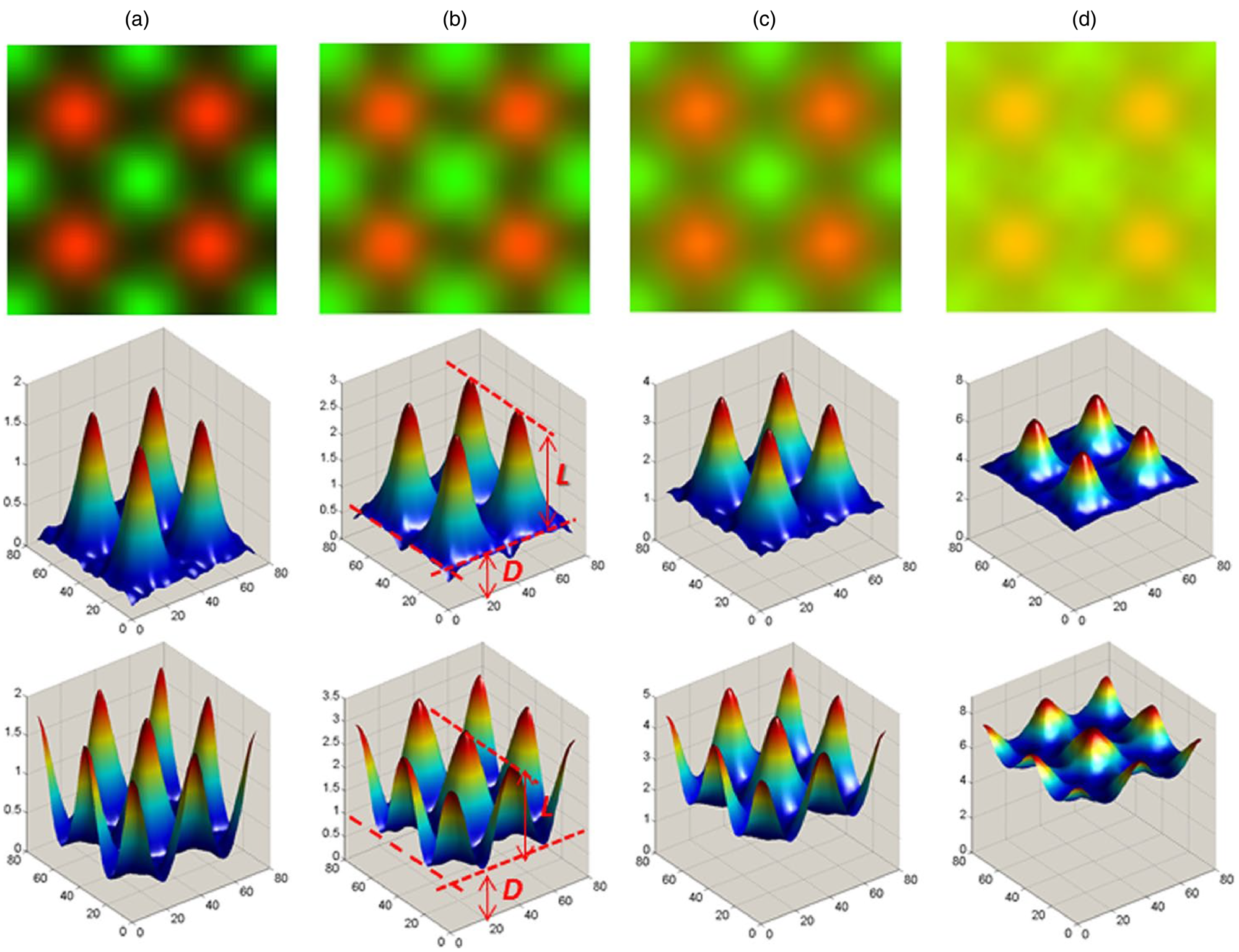
Fig. 24. Averaged 2 × 2 unit-cell XEDS maps (the top panel) (Ti K in red, Sr K + L in green) obtained by using the single-frame scanning method, along with the 3D plots for the Ti K map (the middle panel) and Sr K + L (the bottom panel) at several crystal thickness: (a) 16 nm, (b) 23 nm, (c) 42 nm, and (d) 106 nm. In the middle and bottom panel of (b), the localized (L) and delocalized (D) X-ray level are illustrated. The x- and y-axes in 3D plots are in a pixel number (a pixel size of 0.011 nm). Reproduced from Lu et al. (Reference Lu, Moya, Yuan and Zuo2018).
Future Prospects
The practical realization of aberration corrector on the STEM has transformed the field of electron microscopy. Aberration-corrected STEM has found broad applications in characterizing materials, significantly enhancing our understanding of the micro- and nano-world of matter. With such an enabling tool, we can examine the complexities of structure and chemistry at the atomic scale that have never been achieved before. By conducting in situ or operando experiments within an ac-STEM instrument, we can now follow and understand the reaction or/and transformation pathways that reflect intrinsic material properties. Such atomic-scale understanding of materials behavior leads to crucial insights into developing new materials with desired properties, fabricating new devices with improved performance, or understanding the fundamental physics principles that govern the nano- or atomic-world. The combination of ac-STEM results (e.g., 3D atom coordinates, species, bonding distances, dynamic behavior, etc.) with first-principle calculations has already been, and will continue to be, a driving force for not only a fundamental understanding of material properties but also for enabling new discoveries in material systems and devices. It is anticipated that aberration-corrected electron microscopy, in combination with the related spectroscopy, diffraction, and in situ techniques, will play an indispensable role in the field of materials and engineering including quantum materials and information, energy materials and systems, catalysis and chemical transformation, sensing and detection, and so on.
Although the electron microscopy community has made significant strides in the past 50 years to achieve sub-Ångstrom image resolution (even at low voltages), we still have not developed a practical approach to routinely obtaining 3D atom maps of practical samples with picometer precision in determining atom coordinates (especially at defect sites) and single-atom chemical sensitivity. As discussed in the section “Atomic-resolution electron tomography,” atomic-resolution electron tomography provides a route to resolving 3D atomic structure of materials, leading to investigations of grain boundaries, dislocations, stacking faults, point defects, chemical order/disorder, bond distortion, strain tensors, etc. Atomic-resolution electron tomography, conducted via 4D electron microscopy, significantly expands the application of this method to studying a plethora of materials problems including early-stage nucleation of crystals (Zhou et al., Reference Zhou, Yang, Yang, Kim, Yuan, Tian, Ophus, Sun, Schmid, Nathanson, Heinz, An, Zeng, Ercius and Miao2019). Yang et al. (Reference Yang, Zhou, Zhu, Yuan, Chang, Kim, Pham, Rana, Tian, Yao, Osher, Schmid, Hu, Ercius and Miao2021) extended this powerful approach to determining the 3D atomic positions of an amorphous solid. The authors studied the short-range and medium-range order (SRO and MRO) in a multi-component glass-forming alloy. The combination of advanced computational imaging techniques (e.g., correction for image distortions, enhancement of signal-to-noise ratio, robust reconstruction algorithms, and so on) with a state-of-the-art microscope and accessories is critical to their success in solving a challenging materials problem. This work clearly demonstrates the power of 3D atomic-resolution imaging in addressing grand challenges that may fundamentally confirm or change our view of matter at the level of the most fundamental building block—3D coordinates of atoms.
In addition to further advances in hardware development, robust image calculations and processing algorithms, ultrafast and efficient electron detectors, and ultrafast computers are definitely needed. For example, would it be feasible to display 4D-STEM images on-the-fly when practical samples are examined? Would it be possible to conduct 3D atomic-resolution electron tomography on a large number of heterogeneous structures so that statistically meaningful data can be obtained? As discussed in this review, ultrafast computers and robust image processing algorithms played a critical role in successfully implementing aberration correctors on TEMs/STEMs. One would imagine an ideal scenario that outputs of DFT calculations based on inputs from ac-STEM results can be evaluated on-the-fly. To achieve such a high level of sophistication may require implementation of machine learning (ML) and artificial intelligence (AI)-assisted operation of electron microscopes equipped with ultrafast computers.
Electron microscopists have often faced the challenge of correlating microscopic observations with macro-scale property measurements. Since ultrahigh-resolution imaging experiments usually do not provide excellent statistical data, which is usually required for understanding structure–property relationships, it becomes crucial for developing robust approaches that provide statistically meaningful data. It is enticing to speculate that such a job may be implementable when ML and AI are integrated into routine operations of electron microscopes. The development of AI-assisted synthesis (Coley et al., Reference Coley, Thomas III, Lummiss, Jaworski, Breen, Schultz, Hart, Fishman, Rogers, Gao, Hicklin, Plehiers, Byington, Piotti, Green, Hart, Jamison and Jensen2019; Steiner et al., Reference Steiner, Wolf, Glatzel, Andreou, Granda, Keenan, Hinkley, Aragon-Camarasa, Kitson, Angelone and Cronin2019; Burger et al., Reference Burger, Maffettone, Gusev, Aitchison, Bai, Wang, Li, Alston, Li, Clowes, Rankin, Harris, Sprick and Cooper2020) provided a good example. When electron microscopes can routinely provide statistically meaningful data, the ac-STEM will have a tremendous impact on nanoscience and nanotechnology, nanoscale systems and devices, heterogeneous catalysis, and so on. The breadth of data produced by current ac-STEM experiments, for example, 4D-STEM imaging of dynamic events plus statistical analysis, is already enormous and poses challenges to many aspects of advances in microscopy and materials research. It becomes critical and urgent to identify appropriate approaches to imaging informatics and data science in order to extract valuable structural and chemical information that is buried in massive datasets. Such complex, multilayer and iterative tasks (e.g., rapid segmentation, classification, augmented analysis, diagnosis and error correction, etc.) could not be accomplished without the assistance of ultrafast computers and robust algorithms. Fortunately, electron microscopists have realized this problem and have already started developing innovative approaches to solving such a data science problem (Kalinin et al., Reference Kalinin, Sumpter and Archibald2015; Voyles, Reference Voyles2017; Ziatdinov et al., Reference Ziatdinov, Dyck, Maksov, Li, Sang, Xiao, Unocic, Vasudevan, Jesse and Kalinin2017; Xu & LeBeau, Reference Xu and LeBeau2018; Aguiar et al., Reference Aguiar, Gong, Unocic, Tasdizen and Miller2019; Kalinin et al., Reference Kalinin, Lupini, Dyck, Jesse, Ziatdinov and Vasudevan2019; Laanait et al., Reference Laanait, He and Borisevich2019; Spurgeon et al., Reference Spurgeon, Ophus, Jones, Petford-Long, Kalinin, Olszta, Dunin-Borkowski, Salmon, Hattar, Yang, Sharma, Du, Chiaramonti, Zheng, Buck, Kovarik, Penn, Li, Zhang, Murayama and Taheri2021).
The interaction of an energetic electron beam with matter not only generates various types of signals that carry information about the specimen but also transfers energy/momentum to the specimen which may induce changes in local structure, break chemical bonds, or even cause diffusion/evaporation of atomic species in the probed region of interest (Egerton et al., Reference Egerton, Li and Malac2004; Egerton, Reference Egerton2014, Reference Egerton2019). If the electron-beam-induced degradation effects are not properly accounted for, then erroneous conclusions may be drawn about the structure–property relationships. Electron-beam degradation effects are difficult to predict and should be quantitatively evaluated for each specific type of sample. Electron-beam-induced effects are known to include: (1) knock-on damage, (2) radiolysis, (3) electrostatic charging, and (4) thermal damage caused by electron-beam heating (Egerton et al., Reference Egerton, Li and Malac2004; Egerton, Reference Egerton2019). The mitigation methods, however, are not well-developed especially for radiolysis effects. One usually uses low voltages to minimize the knock-on damage, but simultaneously the radiolysis effects may increase. Even for knock-on damage, we do not have a full understanding on how it occurs at surfaces/interfaces, dopants, adatoms, and various types of defects. For example, radiolytic damage in oxides may arise from excitation of oxygen, leading to bond breakage, desorption of oxygen atoms at the specimen surface, and finally reducing the valence state of the corresponding metallic cations (Jiang, Reference Jiang2016). Such electron-beam-induced radiolysis processes produce dynamic and stable defects, break/form chemical bonds, and displace atoms, resulting in atomic-resolution images that do not represent the original intact specimen at all. Such electron-beam-induced effects become more critical under gas or liquid environment. Therefore, it is critical for the electron microscopy community to quantitatively understand electron-beam-induced effects and to develop effective mitigation approaches. Low-dose electron microscopy approaches have been successfully and extensively used for examining biological systems. Chen et al. (Reference Chen, Odstrcil, Jiang, Han, Chiu, Li and Muller2020) reported that compared with the conventional STEM imaging method, the use of the mixed-state electron ptychography approach not only achieved atomic-resolution with picometer precision but also reduced electron dose by ~50 times. Another approach to low-dose STEM imaging is sparse sampling (Kovarik et al., Reference Kovarik, Stevens, Liyu and Browning2016; Stevens et al., Reference Stevens, Luzi, Yang, Kovarik, Mehdi, Liyu, Gehm and Browning2018; Nicholls et al., Reference Nicholls, Lee, Amari, Stevens, Mehdi and Browning2020). Such a process tempo-spatially separates overlapping of electron-specimen interaction volume, and consequently, an “optimum distance” could be defined to form a scanning image. By using an inpainting method, atomic-resolution images can be reconstructed with an effective low-dose irradiation. High-resolution imaging with extremely low-dose conditions (≤1 e−/Å2) was proposed and reported (Stevens et al., Reference Stevens, Luzi, Yang, Kovarik, Mehdi, Liyu, Gehm and Browning2018).
Electron microscopy at cryo temperatures, with a goal to mitigate electron-beam-induced structural damage, was successfully utilized for studying biological molecules (Taylor & Glaeser, Reference Taylor and Glaeser1974; Fernandez-Leiro & Scheres, Reference Fernandez-Leiro and Scheres2016; Frank, Reference Frank2016; Vinothkumar & Henderson, Reference Vinothkumar and Henderson2016). The incorporation of direct electron detectors with unprecedented speed and sensitivity (McMullan et al., Reference McMullan, Faruqi, Clare and Henderson2014) into modern electron microscopes started a “Resolution Revolution” in molecular biology (Kühlbrandt, Reference Kühlbrandt2014). By combining a highly coherent electron source (low-energy-spread) with energy filtering of inelastically scattered electrons and a high-quality direct electron detector, together with the use of robust reconstruction algorithms, Yip et al. (Reference Yip, Fischer, Paknia, Chari and Stark2020) and Nakane et al. (Reference Nakane, Kotecha, Sente, McMullan, Masiulis, Brown, Grigoras, Malinauskaite, Malinauskas, Miehling, Uchański, Yu, Karia, Pechnikova, de Jong, Keizer, Bischoff, McCormack, Tiemeijer, Hardwick, Chirgadze, Murshudov, Aricescu and Scheres2020) obtained atomic-resolution structures of proteins, enabling the location of individual atoms in a protein to be determined for the first time. These developments are expected to help researchers gain a better understanding, at atomic resolution, of how proteins work in health and disease, leading to the design of better therapeutics. Such a strategy could be used to image inorganic materials or soft materials provided that the specimen holder and the sample are stable enough. The success in atomic-resolution imaging of sensitive battery materials and interfaces by cryo-electron microscopy was clearly a good example (Li et al., Reference Li, Li, Pei, Yan, Sun, Wu, Joubert, Chin, Koh, Yu, Perrino, Butz, Chu and Cui2017; Wang et al., Reference Wang, Huang, Pei, Li, Shi, Yu and Cui2019a, Reference Wang, Li and Meng2019b). Savitzky et al. (Reference Savitzky, Baggari, Clement, Waite, Goodge, Baek, Sheckelton, Pasco, Nair, Schreiber, Hoffman, Admasu, Kim, Cheong, Bhattacharya, Schlom, McQueen, Hovden and Kourkoutis2018) demonstrated that after registering all possible image pairs in a multi-image stack to enhance the signal-to-noise ratio and to correct stage shifts high-quality average images, with information transfer out to 0.07 nm, could be achieved at 300 kV at near liquid nitrogen temperature. The low-temperature mitigation approach provided atomic-resolution STEM images of electron-beam-sensitive metal-oxide nanoparticles with applications in fabricating Li-ion batteries (Tyukalova & Duchamp, Reference Tyukalova and Duchamp2020). High-resolution cryo-STEM imaging was used to detect isolated protein-bound metal ions (Elad et al., Reference Elad, Bellapadrona, Houben, Sagi and Elbaum2017) and to study the fundamental building blocks of enamel (DeRocher et al., Reference DeRocher, Smeets, Goodge, Zachman, Balachandran, Stegbauer, Cohen, Gordon, Rondinelli, Kourkoutis and Joester2020). Goodge et al. (Reference Goodge, Baek and Kourkoutis2020), taking advantage of direct electron detection to enable low-signal experiments, reported atomic-resolution elemental mapping at cryogenic temperatures. It is anticipated that the construction of stable cryo-STEM instruments, in combination with low-dose 4D-STEM imaging, will significantly broaden applications of STEM imaging and associated techniques to research frontiers in physics, chemistry, biology, and materials science and engineering.
Going to extremely low temperatures (e.g., liquid helium temperature) will enable numerous research opportunities for quantum science and technology (Minor et al., Reference Minor, Denes and Muller2019). Since quantum phenomena involve small energies any thermal and/or electron-beam-induced effects at room temperature would wash out the expected quantum behavior. STEM-associated spectroscopy methods at 1–2 meV (or sub-meV) energy resolution would be required for studying quantum phenomena related to small energy excitations. Directly imaging and spectroscopically analyzing quantum materials with atomic-resolution at extremely low temperatures are expected to be highly challenging but the reward could be tremendous. Going to cryo temperatures, however, does not solve other problems such as observing chemical reactions under reaction conditions. Although the ultrafast electron microscopy method (Zewail, Reference Zewail2010; Campbell et al., Reference Campbell, McKeown, Santala, Hawkes and Spence2019) has not achieved atomic-resolution yet, future successful advances in developing atomic-resolution ultrafast electron microscopy would allow us to examine chemical reactions on solid surfaces with significantly suppressed electron-beam-induced effects, to study crystal nucleation and growth processes in liquid environments, to measure atomic diffusion processes at desired sample temperatures, or to explore the atomic configurations of biological molecules and how they control the functions of biological systems. The arrival of atomic-resolution femtosecond or attosecond electron microscopy (if it is achievable) will unlock the mysteries of the dynamic world of matter. Although electron microscopists have made tremendous advances since Ruska's first electron microscope, there are more exciting opportunities in the future to significantly expand the societal impact of atomic-resolution electron microscopy.
Acknowledgments
This work was supported by the National Science Foundation under Grant No. 1955474 (CHE-1955474). The author acknowledges use of the John M. Cowley Center for High-resolution Electron Microscopy at Arizona State University throughout his research career. The author is grateful to Professor David J. Smith of Arizona State University for careful editing of the manuscript and for providing relevant references.


 Open access