


Introduction
Atom probe tomography (APT) has immense potential to enable new insights into the compositional and structural makeup of nanoparticles (NPs). The potential was shown from the first publication (Tedsree et al., Reference Tedsree, Li, Jones, Chan, Yu, Bagot, Marquis, Smith and Tsang2011), where APT was able to provide information on the core–shell structure of unsupported free-standing NPs. For the authors at that time, transmission electron microscopy (TEM) (Jarausch & Leonard, Reference Jarausch and Leonard2009) and X-ray diffraction (XRD) combined could not provide such insights, due to insignificant contrast of the core/shell and peak broadening, respectively. Yet, APT with its single atom analysis principle allows for the analysis of all chemical elements at the nanometer and sub-nanometer scale (Gault et al., Reference Gault, Moody, Cairney and Ringer2012; Larson et al., Reference Larson, Prosa, Ulfig, Geiser and Kelly2013; Miller & Forbes, Reference Miller and Forbes2014; Lefebvre-Ulrikson et al., Reference Lefebvre-Ulrikson, Vurpillot and Sauvage2016).
APT works by successively removing atoms/molecules as ions from a nanoscale, needle-shaped specimen (field ion emitter) using a high electric field. After this field evaporation, the formed ions are then accelerated and projected onto a time-resolved single-atom 2D detector. The 3D structural information is reconstructed using detector hit position and hit sequence while time-of-flight provides the mass-to-charge-state ratio for chemical identification (Gault et al., Reference Gault, Moody, Cairney and Ringer2012; Larson et al., Reference Larson, Prosa, Ulfig, Geiser and Kelly2013; Miller & Forbes, Reference Miller and Forbes2014; Lefebvre-Ulrikson et al., Reference Lefebvre-Ulrikson, Vurpillot and Sauvage2016).
While APT is well suited for the analysis of NPs, due to the mentioned reasons, and despite improvements concerning the spatial resolution (Devaraj et al., Reference Devaraj, Colby, Vurpillot and Thevuthasan2014; Li et al., Reference Li, Bagot, Christian, Theobald, Sharman, Ozkaya, Moody, Tsang and Smith2014; Felfer et al., Reference Felfer, Li, Eder, Galinski, Magyar, Bell, Smith, Kruse, Ringer and Cairney2015; Larson et al., Reference Larson, Giddings, Wu, Verheijen, Prosa, Roozeboom, Rice, Kessels, Geiser and Kelly2015; Lim et al., Reference Lim, Kim, Aymerich Armengol, Kasian, Choi, Stephenson, Gault and Scheu2020), a reliable and repeatable specimen preparation strategy still presents the greatest challenge and limits its utility. The diameter of an APT field ion emitter tip is typically smaller than 150 nm (Gault et al., Reference Gault, Moody, Cairney and Ringer2012; Larson et al., Reference Larson, Prosa, Ulfig, Geiser and Kelly2013; Miller & Forbes, Reference Miller and Forbes2014; Lefebvre-Ulrikson et al., Reference Lefebvre-Ulrikson, Vurpillot and Sauvage2016). They are usually produced out of bulk material using well-established “subtractive methods,” for example, mechanical cutting or ion milling. Generally, samples are prepared by electropolishing (Müller & Tsong, Reference Müller and Tsong1969; Melmed, Reference Melmed1991) or focused ion beam (FIB; Larson et al., Reference Larson, Foord, Petford-Long, Liew, Blamire, Cerezo and Smith1999; Kuhlman et al., Reference Kuhlman, Martens, Kelly, Evans and Miller2001; Miller et al., Reference Miller, Russell and Thompson2005; Thompson et al., Reference Thompson, Lawrence, Larson, Olson, Kelly and Gorman2007).
For NPs, starting with samples smaller than a standard field ion emitter tip, an “additive” specimen preparation process must be established.
Numerous researchers (Lovall et al., Reference Lovall, Buss, Andres and Reifenberger1998; Folcke et al., Reference Folcke, Lardé, Le Breton, Gruber, Vurpillot, Shield, Rui and Patterson2012; Yu et al., Reference Yu, Tong, West, Cheung, Li, Smith, Guo and Tsang2012; Isheim et al., Reference Isheim, Stadermann, Lewis, Floss, Daulton, Davis, Heck, Pellin, Savina, Seidman and Stephan2013; Moutanabbir et al., Reference Moutanabbir, Isheim, Blumtritt, Senz, Pippel and Seidman2013; Xiang et al., Reference Xiang, Chitry, Liddicoat, Felfer, Cairney, Ringer and Kruse2013; Eley et al., Reference Eley, Li, Liao, Fairclough, Smith, Smith and Tsang2014; Felfer et al., Reference Felfer, Benndorf, Masters, Maschmeyer and Cairney2014; Heck et al., Reference Heck, Stadermann, Isheim, Auciello, Daulton, Davis, Elam, Floss, Hiller, Larson, Lewis, Mane, Pellin, Savina, Seidman and Stephan2014; Li et al., Reference Li, Bagot, Christian, Theobald, Sharman, Ozkaya, Moody, Tsang and Smith2014) have published a growing variety of methods for APT NP specimen preparation, as summarized by Felfer et al. (Reference Felfer, Li, Eder, Galinski, Magyar, Bell, Smith, Kruse, Ringer and Cairney2015). Work on applying APT to NPs has intensified in the past 6 years, with a number of successful analyses being published (Larson et al., Reference Larson, Giddings, Wu, Verheijen, Prosa, Roozeboom, Rice, Kessels, Geiser and Kelly2015; Yang et al., Reference Yang, Joyce, Saranu, Hughes, Varambhia, Moody and Bagot2015; Perea et al., Reference Perea, Liu, Bartrand, Dicken, Thevuthasan, Browning and Evans2016; Ironside et al., Reference Ironside, Saxey, Rickard, Gray, McGlynn, Reddy and Marks2017; Kim et al., Reference Kim, Kang, Park, Seol, Ahn, Lee and Choi2018, Reference Kim, Jang, Kang, Ahn, Seol, Kwak, Hatzoglou, Vurpillot and Choi2020; Frierdich et al., Reference Frierdich, Saxey, Adineh, Fougerouse, Reddy, Rickard, Sadek and Southall2019; Barroo et al., Reference Barroo, Akey and Bell2020; Lim et al., Reference Lim, Kim, Aymerich Armengol, Kasian, Choi, Stephenson, Gault and Scheu2020; Qiu et al., Reference Qiu, Zheng, Garg, Chen, Gervinskas, Li, Dunstone, Marceau and Fu2020).
Most methods allow theoretically for application on numerous NP systems, yet reliable evidence from several reports in the literature is not given. Expanding the application from a method on one NP system to another proves to be challenging.
Reasons for the lack of a widely applicable method are the huge variety of NP systems (size, stability, synthesis routines, etc.) and the need to handle each differently and delicately. Additionally, many NPs need to have active states preserved for analysis which can be destroyed by exposure to the environment (Baer et al., Reference Baer, Amonette, Engelhard, Gaspar, Karakoti, Kuchibhatla, Nachimuthu, Nurmi, Qiang, Sarathy, Seal, Sharma, Tratnyek and Wang2008). Even probing energies from standard analysis instruments such as electron microscopy (EM), X-ray photoelectron spectroscopy (XPS), and time-of-flight secondary-ion mass spectrometry (ToF-SIMS) can change shape (Smith et al., Reference Smith, Petford-Long, Wallenberg and Bovin1986), or even melt NPs (Yang et al., Reference Yang, Seah, Gilmore, Morris, Dowsett, Boarino, Sparnacci and Laus2013). This creates a great challenge for any specimen preparation method that aims to be widely applicable.
Most unsupported free-standing NPs are synthesized in a liquid, as a powder, or can be loosened from a substrate. Therefore, a widely applicable specimen preparation method should be able to work with all such NPs. Additionally, for APT analysis, the NPs should be embedded in a matrix (Felfer et al., Reference Felfer, Li, Eder, Galinski, Magyar, Bell, Smith, Kruse, Ringer and Cairney2015) to avoid detachment of entire particles from the tip during the analysis due to the large electrostatic forces. An exception is very small NPs (<10 nm). With decreasing size, adhesion forces can outweigh the electrostatic forces (Tedsree et al., Reference Tedsree, Li, Jones, Chan, Yu, Bagot, Marquis, Smith and Tsang2011; Li et al., Reference Li, Bagot, Christian, Theobald, Sharman, Ozkaya, Moody, Tsang and Smith2014) or even become so large that wetting occurs (Lovall et al., Reference Lovall, Buss, Andres and Reifenberger1998). The embedding can furthermore reduce local magnification effects (Miller & Hetherington, Reference Miller and Hetherington1991; Vurpillot et al., Reference Vurpillot, Bostel and Blavette2000) in large NPs. Yet, for small NPs (<5–10 nm), where interface effects result in trajectory overlaps for the better part of an NP's/phase's dimension (Marquis & Vurpillot, Reference Marquis and Vurpillot2008; Folcke et al., Reference Folcke, Lardé, Le Breton, Gruber, Vurpillot, Shield, Rui and Patterson2012), embedding may also make interpretation of data more challenging. With the exception of such small NPs, the concept of embedding NPs is beneficial for both specimen integrity and data quality. Thus, in the more recent literature by Kim et al. (Reference Kim, Kang, Park, Seol, Ahn, Lee and Choi2018, Reference Kim, Jang, Kang, Ahn, Seol, Kwak, Hatzoglou, Vurpillot and Choi2020), encapsulation combined with (di)electrophoresis NP deposition (Tedsree et al., Reference Tedsree, Li, Jones, Chan, Yu, Bagot, Marquis, Smith and Tsang2011; Li et al., Reference Li, Bagot, Christian, Theobald, Sharman, Ozkaya, Moody, Tsang and Smith2014) showed excellent results.
In some cases, NPs form inside a matrix (Vilayurganapathy et al., Reference Vilayurganapathy, Devaraj, Colby, Pandey, Varga, Shutthanandan, Manandhar, El-Khoury, Kayani, Hess and Thevuthasan2013; Devaraj et al., Reference Devaraj, Colby, Vurpillot and Thevuthasan2014), which lends themselves to standard FIB lift-outs. Otherwise, it is often possible to create a compound specimen where a matrix is provided for a large number of NPs on a flat substrate (Felfer et al., Reference Felfer, Benndorf, Masters, Maschmeyer and Cairney2014; Heck et al., Reference Heck, Stadermann, Isheim, Auciello, Daulton, Davis, Elam, Floss, Hiller, Larson, Lewis, Mane, Pellin, Savina, Seidman and Stephan2014; Larson et al., Reference Larson, Giddings, Wu, Verheijen, Prosa, Roozeboom, Rice, Kessels, Geiser and Kelly2015; Yang et al., Reference Yang, Joyce, Saranu, Hughes, Varambhia, Moody and Bagot2015; Ironside et al., Reference Ironside, Saxey, Rickard, Gray, McGlynn, Reddy and Marks2017; Kim et al., Reference Kim, Kang, Park, Seol, Ahn, Lee and Choi2018, Reference Kim, Jang, Kang, Ahn, Seol, Kwak, Hatzoglou, Vurpillot and Choi2020). This matrix must be void-free, in order to ensure structural integrity. Thus, encapsulation methods have to be used that go around the NPs. This can be achieved with atomic layer deposition (Heck et al., Reference Heck, Stadermann, Isheim, Auciello, Daulton, Davis, Elam, Floss, Hiller, Larson, Lewis, Mane, Pellin, Savina, Seidman and Stephan2014; Larson et al., Reference Larson, Giddings, Wu, Verheijen, Prosa, Roozeboom, Rice, Kessels, Geiser and Kelly2015; Frierdich et al., Reference Frierdich, Saxey, Adineh, Fougerouse, Reddy, Rickard, Sadek and Southall2019), yet undesired changes to NPs may occur due to elevated temperatures. Even if high temperatures can be avoided by using low-melting liquid metals (Kim et al., Reference Kim, Lee, Ahn and Choi2019) or electroplating (Kim et al., Reference Kim, Kang, Park, Seol, Ahn, Lee and Choi2018, Reference Kim, Jang, Kang, Ahn, Seol, Kwak, Hatzoglou, Vurpillot and Choi2020; Lim et al., Reference Lim, Kim, Aymerich Armengol, Kasian, Choi, Stephenson, Gault and Scheu2020), positioning NPs for analysis in a tip using FIB lift-out can be time-consuming.
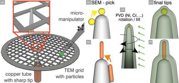
To establish a specimen preparation method that is generally applicable, it is, therefore, desirable to be able to (1) reproducibly pick a single NP and (2) encapsulate it in a matrix for analysis without voids or other flaws in this matrix. The matrix should be reasonably well matched to the field evaporation behavior of the NP. Also, during this process, the NP should not be exposed to any environmental conditions that alter its state (temperature, chemical environment, etc.). In this study, we introduce such a versatile method for NP APT specimen preparation which follows a pick and coat strategy. An overview of the procedure is depicted in Figure 1. First, a desired NP is picked up in situ within a scanning electron microscope (SEM) from a TEM grid with a substrate tip (Fig. 1a). It is then repositioned such that it is located at the very top of the substrate tip (Fig. 1b). Finally, the substrate tip with the attached NP is transferred into an electron beam physical vapor deposition (EB-PVD) system with tilt and rotate capability, where it is coated with the matrix material, for example, Ni or Cr (Fig. 1d). This approach is also feasible with elongated particles, nanorods, or short nanowires as illustrated in Figures 1e and 1f.
Fig. 1. (a) Schematic of NP pick-up off a TEM grid. Main steps during the specimen preparation method based around a pick and coat strategy for spherical NP (b,c) and nanorod (e,f). SEM pick-up (b,e) includes a repositioning step indicated by the arrows connecting pick-up and repositioned, final particle position at substrate tip axis. A supportive coating (d) supports the NP during APT experiments. Final tip architecture (c,f).
In principle, all unsupported free-standing NPs are suitable for this method if they are large enough to be manipulated inside an SEM using a micromanipulator.
Materials and Methods
We introduce our NP APT specimen preparation method with two NP systems: spherical gold nanoparticles (Au-NP) and Ag2Cu2O3 (SCO—Silver Copper Oxide) nanorods (SCO-rod).
Nanoparticle and Nanorod System
The Au-NP were commercially sourced as a citrate-buffered suspension from Sigma-Aldrich (Prod. Number: 742007). The supplier specifies the particles with a diameter of 50 nm and <12% variability in size and shape (https://www.sigmaaldrich.com/catalog/product/aldrich/742007, accessed 02 December 2020).
The SCO-rods were provided as a powder with further information about the synthesis routine and characterization published by Martić et al. (Reference Martić, Reller, Macauley, Löffler, Reichert, Reichbauer, Vetter, Schmid, McLaughlin, Leidinger, Reinisch, Vogl, Mayrhofer, Katsounaros and Schmid2020). Our sample of SCO-rods was polydisperse in size and shape, but they usually had an elliptical cross-section. Rod diameters were reported to be “50–200 nm” and rod lengths varied between “0.52.5 μm” (Martić et al., Reference Martić, Reller, Macauley, Löffler, Reichert, Reichbauer, Vetter, Schmid, McLaughlin, Leidinger, Reinisch, Vogl, Mayrhofer, Katsounaros and Schmid2020). We refer to the SCO-rod sample used in this study as aged because the pristine metal–metal-oxide nanorods formed satellite silver (Ag) particles over storage time. These Ag satellite particles are the characteristic for SCO-rods “aged” in an electrolysis process (bimetallic surface; Martić et al., Reference Martić, Reller, Macauley, Löffler, Reichert, Reichbauer, Vetter, Schmid, McLaughlin, Leidinger, Reinisch, Vogl, Mayrhofer, Katsounaros and Schmid2020). This has no impact in this work, yet must be considered by someone who wants to generalize SCO-rod properties based on data presented here.
Instrumentation
All pick processes were carried out in a Zeiss XB540 FIB-SEM, equipped with a Kleindiek MM3A-EM micromanipulator. The scanning transmission electron microscopy (STEM) imaging was also carried out in this instrument. We used lacey carbon grids supplied by Plano GmbH, Germany, as carriers for the NPs. We used tungsten (W) needles as substrate tips, which were produced by electropolishing a W wire in 5% sodium hydroxide (NaOH) aqueous solution. A polishing voltage of 5 V alternating current (AC) was used, while immersing the wire into the NaOH solution. Typical W substrate tips for pick-up had a radius of curvature (r c) of around 30 nm and a shank angle (α) of around 15°.
The coating of the specimen was done in a custom-built EB-PVD unit, as illustrated in Figure 2a. It consists of an ultra-high vacuum (UHV) chamber pumped by an 80 L/s turbomolecular pump, with load lock, through which a sample can be inserted. The UHV system keeps the base pressure around 2.0 × 10⁻⁸ mbar. In the chamber, a dual-source electron beam evaporator is mounted (e-flux2 Dual Evaporator, Tectra Physics, Germany). In this study, only chromium (Cr) was used as the target material for coating, but any material that can be e-beam evaporated can be used. Inside the deposition unit, the specimen is mounted on a dual-axis magnetically coupled manipulator (specimen mount). This specimen mount allows for tilting and rotating the specimen as illustrated in Figure 2b. By tilting and rotating the sample during coating, an even coating can be deposited on a tip-shaped specimen. The thickness of the coating is monitored during the process with a quartz microbalance mounted behind the sample (Fig. 2a). Once the desired thickness was achieved, the coating was stopped.

Fig. 2. (a) Tilt and rotate PVD setup. The direction of the PVD deposition with respect to the specimen mount is indicated by a vertical, green arrow. Deposition progress is monitored by the microbalance behind the specimen mount. Load-lock for specimen position is indicated by a placeholder text “load-lock” to the right. (b) Specimen mount at load-lock. Rotating arrows indicate tip rotation around its axis and tip tilting around the dotted lined axis.
Procedure Following a Pick and Coat Strategy: Spherical Nanoparticle
In this work, the main steps involved in preparing an NP for APT analysis are:
(1) deposition of NPs on a lacey/holey amorphous carbon film-coated TEM grid (TEM grid);
(2) NP pick-up and repositioning (Figs. 1b, 1e, “SEM pick-up”) following an in situ SEM lift-out strategy (“stamping transfer”; Przybilla et al., Reference Przybilla, Apeleo Zubiri, Beltran, Butz, Machoke, Inayat, Distaso, Peukert, Spiecker and Schwieger2018); and
(3) coating using our customized tilt and rotate EB-PVD setup (Figs. 1c, 1d, 1f).
In the following, each step is explained in more detail.
NP deposition: For Au-NPs, electrospray deposition (Lenggoro et al., Reference Lenggoro, Okuyama, Fernández de la Mora and Tohge2000; Kebarle & Verkerk, Reference Kebarle and Verkerk2009; Soliwoda et al., Reference Soliwoda, Rosowski, Tomaszewska, Tkacz-Szczesna, Celichowski and Grobelny2015) was used to distribute them on a lacey carbon grid. The original suspension was mixed with pure methanol (Sigma-Aldrich) at 1:1. The characteristic red suspension color remained although it did appear diluted. Thus, the Au-NPs remained colloidally stable after mixing. A silica capillary with tapered tip (360 μm outer diameter (OD), 50 μm inner diameter (ID), New Objectives, Inc., USA) was cut to a length of 5 cm and attached to a PEEK tubing [OD = 1.6 mm (1/16 inches), ID = 0.5 mm (0.20 inches)] using MicroFerrules (IDEX H&S Corp., USA). The TEM grid was placed on a grounded copper substrate at a distance of 5 μm to the spray capillary. Gravity was used to evenly feed the liquid through tubing toward the spray capillary. For this purpose, a height difference of suspension reservoir and spray capillary of 65 cm (liquid flow rate about 40 μl/h) was set. A Taylor cone typically formed at 3–4 kV with a spray current measured around 60 nA. The deposition was terminated after 10 min with the carbon layer of the TEM grid facing up to the spray plume.
The SEM pick-up and repositioning of the NPs require contrary and independent movement of substrate tip and NP/TEM grid inside the Zeiss XB540 Crossbeam chamber. Therefore, the TEM grid was crimped to one side of a copper tube extender (see Supplementary material A) that fits to a micromanipulator (MM3A-EM, Kleindiek Nanotechnik GmbH, Germany) mount. The substrate tip was mounted to the SEM stage as illustrated in Figure 1a.
We followed the published pick and place SEM strategy (“stamping transfer”; Przybilla et al., Reference Przybilla, Apeleo Zubiri, Beltran, Butz, Machoke, Inayat, Distaso, Peukert, Spiecker and Schwieger2018), which was originally introduced for electron tomography (ET). Unlike the original authors, we focused on NPs at amorphous carbon edge positions. Figure 3a shows an SEM image of spherical Au-NPs deposited on a lacey carbon grid with a substrate W tip in the background. The red ring highlights an Au-NP at a lacey carbon edge side facing toward the tip. Figure 3b shows this particle transferred to the substrate tip's apex after pick-up.

Fig. 3. SEM view before (a) and after (b) SEM pick-up. Foreground: carbon lacey grid with Au-NPs. Background: field ion emitter tip (W tip) from top view pointing out of the image plane. Ring overlay in (a) indicates Au-NP at lacey carbon edge position that is transferred to tip apex in (b). Arrows in (a) indicate other suitable Au-NPs at edge positions for pick-up. Au-NPs sitting on the tip-faced side of the lacey carbon grid (solid line arrow) are easier to manipulate than Au-NPs on the opposite side (dotted line arrows).
Other promising NP candidates for pick-up are indicated by arrows in Figure 3a. Within this setup, well-suited NPs are facing toward the tip (solid line arrow) rather than toward the detector (dotted line arrows). With NPs facing toward detector, it is more likely that contact of the tip is mistakenly made with the grid, not with the NP.
As a rule of thumb, we suggest substrate tips with an r c equal to, or smaller than the radius of the NPs (tips used for Au-NPs and SCO rods: r c ≈ 30 nm, α ≈ 15°). With increasing tip dimensions, it becomes more challenging to contact only the NP.
The NPs tend to stick to the lacey carbon film in their original position. We found it helpful to loosen a NP by pushing it in direction of the grid support (see Supplementary material B). From our experience, tips with small r c (<30 nm) and α (<15°) deflect elastically around/under particles during loosening. This can be avoided by using a lower (with regard to tip apex), stiffer region of the tip as a contact point with the NP. After loosening, the NP can be easily picked off and moved along the TEM grid and substrate tip for repositioning right at the tip apex (compare Figs. 3, 4a; Supplementary material C).
After SEM pick-up, the specimens were transferred into the customized tilt-and-rotate EB-PVD setup. We used Cr as a target with a purity of 99.5 wt% (HMW-Hauner, Germany). Mean deposition rates were measured to be ~0.1 nm/s. Pressure peaks during deposition were below 1.0 × 10⁻⁷ mbar with pressures of 1–5 × 10⁻⁸ mbar during most of the deposition time. In the case of our Au-NP specimen, we deposited 23 ± 3 nm Cr.

Fig. 4. EM images of different steps during the specimen preparation method (a–c) for a spherical gold Au-NPs and STEM images for other samples after EB-PVD coating. (a) SEM image of Au-NP after pick-up and repositioning. (b,c) STEM images of the same specimen after EB-PVD supportive coating from two view perspectives being 90° rotated with respect to each other. (d,e,f,g,h,i) EB-PVD-coated samples from perspectives 90° rotated for another Au-NP specimen, copper selenide NP, and SCO-rod, respectively. If not specified, scale bars represent a length of 200 nm.
The fabrication time of such an embedded NP at a tip apex was empirically between under an hour and up to 3 h per tip [excluding tip polishing (~10 min) and STEM imaging]. The time deviation derived mainly by the number of pick-up attempts on different NPs per tip.
The number of attempts usually varied from one to three per NP, but could go up to 10 attempts per tip in the case of nanorods. Typical reasons for an attempt failure were pushing NPs on top of the grid and failing to loosen the particle. The former resulted in particles being placed at a position out of the tip's reach. The latter was associated with being geometrically unable to contact only the particle and not the grid with the tip. In this case, the grid was pushed by the tip, rather than the particle being moved with respect to the grid. In addition, nanorods regularly flew away of tip/grid during repositioning.
Time was well invested in choosing the best-suited particle candidates on the TEM grid (red circle solid line arrow in Fig. 3), which took about ~5 min per attempt. This depends on particle density and distribution of individual particles (agglomeration) on the grid. As a rule of thumb, multiple suitable NP candidates should be available in a similar image width (2 to 5 μm) as seen in Figure 3. Otherwise, looking for suitable particles becomes the time-determining activity for the procedure.
Positioning a tip nearby an NP, loosening, and repositioning the NP took around 10–20 min. Coating of NP took about 10 min (depending on layer thickness and deposition rate), but additional time for transferring NPs from SEM to EB-PVD setup and conditioning target material took added ~15 min.
The specimens were then stored in vacuum desiccators before they were transferred to a CAMECA LEAP 4000X HR (reflectron) for APT analysis. The Au-NP specimens were field evaporated in laser pulsing mode at a pulse rate of 100 kHz and a detection rate of 0.5%. The temperature was set to 50 K, and a laser pulse energy of 100 pJ was applied. APT reconstruction was performed using IVAS® 3.6.8 (CAMECA Instruments, Inc., USA) with parameters that resulted in reconstructions matching the corresponding EM images closely. Data visualization and post-processing were performed using in-house MATLAB® (MathWorks, Inc., USA) scripts (https://github.com/peterfelfer/Atom-Probe-Toolbox) which were run in the R2019b version of MATLAB®.
Procedure Following a Pick and Coat Strategy: Nanorod
SCO-rods were distributed on the lacey carbon grid by simply shaking a grid in a container containing a spatula-tip of SCO-rod powder. This led to enough SCO-rods adhering to the grid for pick-up.
The SEM pick-up for the SCO-rods (see Supplementary material D) works identically to the spherical NPs, apart from the repositioning step. The tip was put into contact with one SCO-rod end, while the other end of the rod was put in touch with the lacey carbon. By moving the tip and grid in opposing z-directions while adjusting the x and y alignment, the tip was placed directly beneath the grid-particle contact point with the SCO-rod aligned with the axis of the tip. By further increasing the z-difference of tip and grid, either the SCO-rod stuck to the tip, to the grid, or flew away. With a couple of attempts for each substrate tip, we consistently produced free-standing SCO-rods sitting at the end of a substrate tip and aligned with the tip axis (see Fig. 6b; Supplementary material E).
In order to preserve this free-standing position, the contact point of substrate tip and SCO-rod was supported with a thin Pt film using the electron beam and gas injection system (GIS). Then, a Cr layer of 62 ± 29 nm was deposited using EB-PVD.
SCO-rod specimens were field evaporated in laser pulsing mode at a pulse rate of 100 kHz, detection rate of 0.4%, temperature set to 52 K, and a laser pulse energy of 75 pJ. Data analysis was similar to that of the Au-NPs.
Results and Discussion
Spherical Au-NP
A spherical Au-NP sample produced by citrate reduction (Turkevich et al., Reference Turkevich, Stevenson and Hillier1951) was used for proofing the concept of the presented method. The high mass density of Au allows for an easy distinction of NP and W substrate tip from a lighter coating material in transmission electron imaging.
After SEM pick-off, described in the section (Procedure Following a Pick and Coat Strategy: Spherical Nanoparticle), the same Au-NP from Figure 3 is shown in Figure 4a in a side view. After coating with Cr, the correct positioning of the Au-NP was confirmed using transmission electron imaging. This is exemplarily depicted in Figure 4b and c, with view directions rotated 90° around tip axis with respect to each other. Here, the supportive layer has a thickness of 55 ± 9 nm, similar to the Au-NP diameter.
After this final processing step, the overall shape remains that of a sharp tip, albeit with a higher apex radius. The position of the Au-NP is at the substrate tip axis with a few degrees offset. This specimen structure can be reproduced as can be seen for another Au-NP (Figs. 4d, 4e; view directions rotated 90°), a larger copper selenide particle (Figs. 4d, 4g; view directions rotated 90°), and a rod-shaped SCO-rod (Figs. 4h, 4i; view directions rotated 90°).
Of the four-layer sides visible in the two 90° views (Figs. 4b, 4d), three sides are uniformly thick and follow the underlying form. One side (Fig. 4e, right) is thicker. This may be caused by manual, uneven tip rotation, which will soon be replaced in our system with motorized tip rotation.
The PVD process results in a rougher surface compared with the preparation via FIB or electropolishing. The roughness is a result of PVD's nucleation and growth mechanism (Movchan & Demchishin, Reference Movchan and Demchishin1969; Thornton, Reference Thornton1974; Messier et al., Reference Messier, Giri and Roy1984; Singh & Wolfe, Reference Singh and Wolfe2005). In Figures 4b and 4c, polycrystallinity can be seen with grains starting to grow in a columnar fashion, as is predicted from PVD's structural evolution. Nanosized voids from intergrain shading were reported even at low deposition rates (0.1 nm/s; Thornton, Reference Thornton1974; Messier et al., Reference Messier, Giri and Roy1984).
A 3D atom map of the APT reconstruction of such an Au-NP specimen with identical architecture as Figure 4 (see Supplementary material F) is presented in Figure 5. For this reconstruction, we used the Geiser et al. (Reference Geiser, Larson, Oltman, Gerstl, Reinhard, Kelly and Prosa2009) reconstruction protocol with the field evaporation voltage curve as an estimate for the specimen radius. For this heterogeneous compound specimen, this is obviously not an optimal scenario. We anticipate the development of a more tailored reconstruction algorithm in the near future.

Fig. 5. APT reconstruction of spherical Au-NP. Each section (a–d) shows reconstructed atom positions for the elements Au, Cr, W, and O, respectively.
The main elements Au (NP, Fig. 5a), Cr (supportive layer, Fig. 5b), and W (substrate tip, Fig. 5c) are presented with all recorded detector hits within the mass-to-charge range of the respective element, with each dot representing the reconstructed position of an atom.
From a data quality standpoint, this reconstruction is already well suited for the analysis of an NP's chemical composition (in this case only Au). Yet, the detailed spatial analysis is defective. This is owing to the fact that pure Au is prone to sudden bursts in the evaporation rate with the field evaporation temporarily being concentrated to certain areas of the Au-NP (“patchy” field evaporation). In the experience of the authors, this is specific to specimens from Au and other soft metals such as Cu and does not occur in most other materials, such as the deposited chromium layer by itself.
In APT, well-known issues with multi-phase samples (e.g. here: coating, NP, substrate tip) are reconstruction artifacts based around differences in evaporation fields, which is also the case for NP analysis in particular (Folcke et al., Reference Folcke, Lardé, Le Breton, Gruber, Vurpillot, Shield, Rui and Patterson2012; Devaraj et al., Reference Devaraj, Colby, Vurpillot and Thevuthasan2014; Heck et al., Reference Heck, Stadermann, Isheim, Auciello, Daulton, Davis, Elam, Floss, Hiller, Larson, Lewis, Mane, Pellin, Savina, Seidman and Stephan2014). In the Au-NP data shown in Figure 5a, the reconstruction shows a discontinuous surface consisting of spikes. Yet, from the EM image (Fig. 4a), a smooth, continuous surface is to be expected.
These spikes were recently discussed by Kim et al. (Reference Kim, Jang, Kang, Ahn, Seol, Kwak, Hatzoglou, Vurpillot and Choi2020) for Pd@Au core–shell NPs in an Ni matrix. Based on a simulation model (Vurpillot et al., Reference Vurpillot, Gaillard, Da Costa and Deconihout2013), they have shown that field evaporation differences between matrix and NP can explain such spikes due to trajectory aberrations. According to basic evaporation theory calculations, the combination of Cr [28 V/nm (Miller & Forbes, Reference Miller and Forbes2014)] and Au [53 V/nm (Tsong, Reference Tsong1978)] phases should have a similar “spiky” outcome, although these zero-barrier evaporation fields do not include defects such as grain boundaries and interphase boundaries, nor the influence of the laser.
We also assume that the high oxygen content in the Cr coating, possible adhesion problems, and/or nanovoids may have led to delamination of large pieces of the coating as well as microfractures in the Cr coating during the APT experiment. Such specimen fraction events can be seen in the reconstruction in Figure 5b by the two distinct Cr density “steps” in the analysis z-direction. Parts of the tip fractured, yet measurement continued to run. Microfractures may also explain spikes at the Au-NP surface due to sudden local trajectories changes
The high amount of residual oxygen (order of 5–10 wt%) in the Cr layer may lead to a less structurally sound specimen compared with higher purity Cr coatings such as in work by Felfer et al. (Reference Felfer, Benndorf, Masters, Maschmeyer and Cairney2014). This could be improved by a better vacuum in the coating unit. Even at the low vacuum pressures within the PVD chamber (1–5 × 10⁻⁸ to 1 × 10⁻⁷ mbar), the low deposition rates used in this work of less than a monolayer per second (0.1 nm/s) provides plenty of time for Cr to absorb residual O. Yet, higher deposition rates were not used to minimize the formation of intergranular voids due to intergrain shading (Thornton, Reference Thornton1974). Improvements such as optimizing the EB-PVD deposition (deposition rate, deposition tilt angle, vacuum), or following a different coating procedure (Larson et al., Reference Larson, Giddings, Wu, Verheijen, Prosa, Roozeboom, Rice, Kessels, Geiser and Kelly2015; Kim et al., Reference Kim, Kang, Park, Seol, Ahn, Lee and Choi2018; Frierdich et al., Reference Frierdich, Saxey, Adineh, Fougerouse, Reddy, Rickard, Sadek and Southall2019) will be taken into account in the following studies.
Ag2Cu2O3 Nanorod
As already mentioned above, the presented method is also suitable for elongated NPs such as nanorods or short nanowires. This is demonstrated on an SCO-rod used as a catalyst template structure in carbon dioxide (CO2) reduction (Martić et al., Reference Martić, Reller, Macauley, Löffler, Reichert, Reichbauer, Vetter, Schmid, McLaughlin, Leidinger, Reinisch, Vogl, Mayrhofer, Katsounaros and Schmid2020). For such an SCO-rod, the different steps during this method's procedure are shown in Figure 6. These SCO-rods present a more challenging situation since they are typically intergrown and have satellite particles attached to them.

Fig. 6. EM images of different steps during the specimen preparation method for SCO-rods. (a) View before SEM pick-up: TEM grid lacey carbon film string with SCO-rods and substrate tip pointing out of the image plane. (b) SEM image of SCO-rod after pick-up and repositioning. (c,d) STEM images of the same specimen after EB-PVD supportive coating from two view perspectives being 90° rotated with respect to each other.
To analyze one of the SCO-rods, first we identified the SCO-rod of interest on the lacey carbon grid, as shown in Figure 6a. We then picked the SCO-rod up and repositioned it as described under the section “Procedure following a pick and coat strategy: nanorod.” The resulting final alignment is shown in Figure 6b in side view. At the intersection point of SCO-rod and substrate tip, a subtle GIS Pt layer deposition can be seen. This stabilized intersection point keeps the rod in position for subsequent processing steps.
In Figure 6b, two satellite particles are visible on the upper region of the SCO-rod. Using TEM energy-dispersive X-ray spectroscopy (EDX), Martić et al. (Reference Martić, Reller, Macauley, Löffler, Reichert, Reichbauer, Vetter, Schmid, McLaughlin, Leidinger, Reinisch, Vogl, Mayrhofer, Katsounaros and Schmid2020) showed for such particles to contain almost exclusively Ag. The rod–substrate contact point is at the side of the SCO-rod and substrate tip rather than exactly at the tip apex.
Figures 6c and 6d show transmission electron images of the specimen after Cr coating, with each image rotated 90° along the tip axis with respect to each other. Here, the supportive layer has a thickness of around 62 ± 29 nm.
After this final processing step, the overall specimen shape is suitable as a field ion emitter. The structure consists of two regions: the particle/rod region and the substrate tip contact region. In both regions, the EB-PVD layer follows the underlying outline of the assembled specimen, but in the lower region, the specimen thickness is already too large to be captured in the APT experiment. Also, the SCO-rod is slightly tilted with respect to the analysis axis, but we do not expect this to influence the analysis.
In the subsequent APT experiment, a section of the above specimen could be captured. 3D atom maps of the copper (Cu) and Ag atoms of this section are presented in Figures 7b and 7d, with the views rotated 90° with respect to each other.

Fig. 7. (a,c) STEM images of the specimen SCO-rod from two view perspectives being 90° rotated with respect to each other. Rectangular overlays mark the position of the reconstructed APT data in (b,d). ROI box was closely fitted by hand around Ag and Cu data, which helps to visualize the tilt of the rod at given view perspective. (e) Histogram of the ion hit density on the detector (field desorption map).
The corresponding region in the specimen is marked with a red rectangular overlay in Figures 7a and 7c. This location correspondence can be made by identifying the individual Ag satellite particle on the surface of the SCO-rod. This satellite particle is visible in the APT reconstruction (Figs. 7b, 7d) and the EM images at the bottom right corner of the regions marked by the red rectangles (Figs. 7a, 7c).
In the reconstruction, the distribution of Ag and Cu is captured for the surface of the SCO-rod and for the interior. It can be seen that not one uniform solid solution is present, but rather some segregation into Cu-rich and Ag-rich volumes. While Cu is found predominantly in the interior, Ag is mainly present at the SCO-rod surface. However, the 3D reconstruction displayed is still suffering from some artifacts, notably local magnification (Miller, Reference Miller1987; Vurpillot et al., Reference Vurpillot, Bostel and Blavette2000). This is an effect whereby a locally lower density of atoms is recorded on the detector due to a higher curvature of the specimen, or vice versa in the case of the SCO-rod. This can be observed in the field desorption map (FDM) in Figure 7e, which is a histogram of the detector's ion hit density. This uneven hit density is partially caused by the apparent lower evaporation field of the SCO-rod compared with the Cr matrix. For APT data in general, a higher hit density for a given phase can result from a surrounding matrix of a relatively higher evaporation field (Vurpillot et al., Reference Vurpillot, Bostel and Blavette2000; Beinke & Schmitz, Reference Beinke and Schmitz2018). Evaporation fields of the involved metal elements Cr, Cu, and Ag [28, 30, and 27 V/nm, respectively; Miller & Forbes, Reference Miller and Forbes2014) match closely and cannot explain such a density observed in the FDM. Here, it is important to note that it remains unclear to what extent the metal–metal-oxide has transitioned to metal during aging. Since the evaporation field of SCO as metal–metal-oxide and metal-oxides has not been investigated, the presented data suggest that it is smaller than that of Cr.
Such a relative lower evaporation field of SCO compared with Cr can then also explain the difference in dimensions between the reconstruction (Figs. 7b, 7d) and the EM images (Figs. 7a, 7c). Additionally, the shape of the SCO-rod appears more oval, beyond what is observed in STEM images (Fig. 6). This may be caused by the “step” between nanorod and substrate tip visible in Figure 7c which causes unidirectional field compression.
Specimen Preparation Potential and Limitations
In this work, we introduced a new method that follows a pick and coat strategy for NP APT specimen preparation. The application of this method was shown for two different types of exemplary nanomaterial systems, which supports this method's versatility in its application to various NP systems. The mechanical manipulation of NPs does not rely on specific NP properties, such as its colloidal stability and mobility in an electrical field (Li et al., Reference Li, Bagot, Christian, Theobald, Sharman, Ozkaya, Moody, Tsang and Smith2014; Kim et al., Reference Kim, Kang, Park, Seol, Ahn, Lee and Choi2018). Instead, if NPs can be deposited onto a TEM grid, this method will produce suitable specimens for APT.
Another key feature of our method is the well-defined specimen architecture in combination with its reproducibility. The region of interest, the NP, is carefully placed within the first hundred nanometers of a field ion emitter tip right at the tip axis (field of view of APT). This is significantly more reproducible than with lift-out strategies (Felfer et al., Reference Felfer, Benndorf, Masters, Maschmeyer and Cairney2014; Frierdich et al., Reference Frierdich, Saxey, Adineh, Fougerouse, Reddy, Rickard, Sadek and Southall2019), or (di)electrophoresis (Li et al., Reference Li, Bagot, Christian, Theobald, Sharman, Ozkaya, Moody, Tsang and Smith2014). There, positioning of the NP with respect to the surrounding matrix is more difficult or impossible in case of the latter. This reproducibility could significantly aid the development of a custom reconstruction algorithm tailored to this well-defined structure. The algorithm could take the shape and position of the NP in a simplified manner as an input to correct trajectory aberrations based on mismatching evaporation fields.
Other advantages of the presented method derive from the picking method of individual NPs that was adapted from Przybilla et al. (Reference Przybilla, Apeleo Zubiri, Beltran, Butz, Machoke, Inayat, Distaso, Peukert, Spiecker and Schwieger2018). The observation of NPs before pick-up makes it possible to select specific NPs for analysis. A certain size, shape of polydisperse NP solution, or other physical properties (Koh et al., Reference Koh, Bao, Khan, Smith, Kothleitner, Nordlander, Maier and McComb2009; Nicoletti et al., Reference Nicoletti, de la Peña, Leary, Holland, Ducati and Midgley2013; Paul et al., Reference Paul, Kotagiri, Ganguly, Parashari, Courtois, Winkelmann and Gupta2020) may be of extensive interest for further investigation. Such complementary physical property testing could also help making APT measurements statistically more relevant. For this, compositional or structural features can be systematically linked to certain physical properties. Complementary EM (Arslan et al., Reference Arslan, Marquis, Homer, Hekmaty and Bartelt2008; Grenier et al., Reference Grenier, Duguay, Barnes, Serra, Haberfehlner, Cooper, Bertin, Barraud, Audoit, Arnoldi, Cadel, Chabli and Vurpillot2014; Przybilla et al., Reference Przybilla, Apeleo Zubiri, Beltran, Butz, Machoke, Inayat, Distaso, Peukert, Spiecker and Schwieger2018; Fletcher et al., Reference Fletcher, Moody and Haley2020) of intermediate or final specimen fabrication steps may be used to assist or improve reconstruction and, thus, data quality. Adopted reconstruction algorithms that are based on accurately knowing the ion trajectories at any point during the APT experiment may be used. For this, full-scale simulation tools (Oberdorfer et al., Reference Oberdorfer, Eich and Schmitz2013; Vurpillot et al., Reference Vurpillot, Gaillard, Da Costa and Deconihout2013; Rolland et al., Reference Rolland, Vurpillot, Duguay and Blavette2015; Fletcher et al., Reference Fletcher, Moody and Haley2019) can predict field ion emitter tip shape changes based on the tip feature's (phases, particles) and shape known by correlative EM. This leaves only the evaporation field of the NP and coating as parameters in an otherwise well-characterized system. These parameters may be iteratively optimized to reproduce features from EM (Fletcher et al., Reference Fletcher, Moody and Haley2020).
From 22 conducted APT measurements three reasonable large data sets (approx. >1–3 million atoms at the region of interest) were measured, two of them are presented here. Specimen integrity is the limiting factor. Reasons for this are related to the EB-PVD coating quality (adhesion, voids, oxygen content) and are discussed above.
We like to emphasize that an additional four data sets clearly started to measure NPs right before the specimens fractured during APT. Seven specimens out of twenty two (32%) started to measure the NP within the limits of the detector. This states that the concept of placing NPs right at the tip apex works well and is a benefit to this method. Comparable data on success rates for other techniques (FIB lift-out, dielectrolysis) described in introduction at early stages (proof of concept) were not found. For comparison, it should be taken into account that this method's success rate is applied to measuring one specific, possibly preselected particle, which is beneficial for systematic studies.
The main requirement for the nanomaterial to be analyzed is that it needs to be able to be dispersed on a lacey carbon grid or a similar support, for example, by drop casting or by simply dipping the grid into a powder. The other main limitation is the scale at which nanosized objects can be manipulated in the SEM. In our setup, NPs with sizes >50 nm could be comfortably manipulated, but for smaller NPs, the time to manipulate one particle was either excessively high (range of 20–50 nm) or manipulation was not possible in a meaningful way (<20 nm). This is both owing to the resolution of the SEM, and the motion of the micromanipulator. In order to enable SEM pick-up, the surfaces of the substrate tip (Matope et al., Reference Matope, Van der Merwe and Rabinovich2013), TEM grid film (Zhou et al., Reference Zhou, Wang, Zhang, Zhao, Li and Yan2009), or NPs (Neouze & Schubert, Reference Neouze and Schubert2008) may need to be modified. In the present work, such modifications were unnecessary.
The final data quality, that is, spatial resolution of the 3D reconstruction of the data acquired from the specimens in this paper, depends crucially on our ability to create a suitable model of the field evaporation. This is not trivial, since current sequential back-projection reconstruction algorithms (Bas et al., Reference Bas, Bostel, Deconihout and Blavette1995; Geiser et al., Reference Geiser, Larson, Oltman, Gerstl, Reinhard, Kelly and Prosa2009) assume simplified sphere on cone field ion emitter tip shapes. Some of these issues can be mitigated by proper sample design, that is, choice of coating and initial cone shape. This influences how well the idealized sphere on cone tip shape is reproduced in the actual experiment until an adapted reconstruction algorithm makes this potentially redundant.
Conclusions
The presented method for NP APT preparation involves (1) mechanically picking up single NPs off a TEM grid with a field ion emitter tip in an SEM and (2) subsequently coating the specimen with a protective layer (several 10 s of nm) using a custom-built PVD system with tilt and rotate ability.
Different types of NPs (metals, metal-oxides), with different shapes (sphere, rod), provided as powder or out of solution, were shown to be successfully placed at the tip apex of a substrate field ion emitter tip. The subsequent coating defines the final NP APT specimen size. NPs can be tailored to the field of view of APT measurement. A restriction is the NP size must be larger than ~50 nm, since handling of NPs in an SEM is limited by the SEM resolution.
The key advantage of this method is that the NP can be positioned within the first hundred nanometers of the tip apex in a reproducible way. At the current stage of method development, two different NP systems were successfully measured in APT, which proves the method's potential to expand its application to other free-standing NP systems. Although sample preparation is reproducible, running successful APT experiments proved to be challenging due to failing specimen integrity. In order to increase success rates of the APT experiment, the following work must improve coating quality (optimize PVD process, or use of different technique, such as ALD) to exclude defects and improve adhesion. Adjusting substrate tip, particle, and coating with respect to each other may improve data quality by reducing standard reconstruction artifacts. The possibility to preselect a specific NP based on shape, size, physical properties, etc., using correlative microscopy derives from integrating the “stamping-transfer” (Przybilla et al., Reference Przybilla, Apeleo Zubiri, Beltran, Butz, Machoke, Inayat, Distaso, Peukert, Spiecker and Schwieger2018) and allows for systematic studies.
Future work focuses on a specialized, adapted reconstruction algorithm that takes advantage of the method's well-defined tip structure to correct for standard artifacts. By combining such a reconstruction algorithm with this method, reliable NP APT interface analysis may be in reach.
Supplementary material
To view supplementary material for this article, please visit https://doi.org/10.1017/S1431927621000465.
Acknowledgments
This work was funded by the Deutsche Forschungsgemeinschaft (DFG – German Research Foundation) under project FE 1593/2-1. Furthermore, the authors gratefully acknowledge financial support by the DFG via the research training group GRK 1896 “In Situ Microscopy with Electrons, X-rays and Scanning Probes.” The authors thank N. Martić at Siemens Gas and Power GmbH & Co. KG, 91058 Erlangen, Germany, for providing the SCO nanorods.


 Open access