


No CrossRef data available.
Article contents
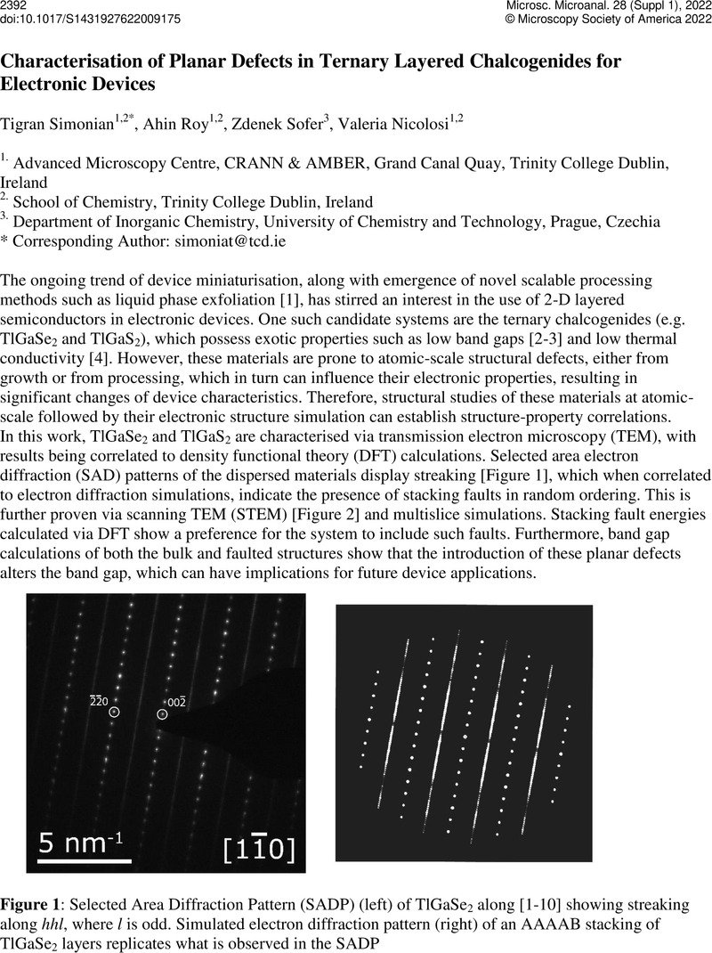
Characterisation of Planar Defects in Ternary Layered Chalcogenides for Electronic Devices
Published online by Cambridge University Press: 22 July 2022
Abstract
An abstract is not available for this content so a preview has been provided. As you have access to this content, a full PDF is available via the ‘Save PDF’ action button.
- Type
- Advanced Imaging and Spectroscopy for Nanoscale Materials
- Information
- Copyright
- Copyright © Microscopy Society of America 2022
References
Cengiz, A. et al. , Semicond. Sci. Technol. 33 (2018).10.1088/1361-6641/aac97bCrossRefGoogle Scholar
Duman, S. and Gürbulak, B., Phys. Scr. 72 (2005), p. 79.10.1238/Physica.Regular.072a00079CrossRefGoogle Scholar
Shim, Y., Kawabata, T., Wakita, K. and Mamedov, N., Phys. Status Solidi B, 252 (2015), p. 1254.10.1002/pssb.201400342CrossRefGoogle Scholar
 You have
Access
You have
Access