


Introduction
Knowledge of interfacial energy values may be necessary when solving microstructural or metallurgical challenges in demanding the industrial applications of commercial CuZn alloys where the combinations of strength, machinability, and corrosion resistance are required (Zhao et al., Reference Zhao, Liao, Horita, Langdon and Zhu2007; Zhang et al., Reference Zhang, Duan, Li and Zhang2008; Igelegbai et al., Reference Igelegbai, Alo, Adeodu and Daniyan2017; Choucri et al., Reference Choucri, Zanotto, Grassi, Balbo, Ebn Touhami, Mansouri and Monticelli2019; Gu et al., Reference Gu, Ni and Song2019; Zaynullina et al., Reference Zaynullina, Alexandrov and Wei2019). Nucleation, growth, and coarsening of precipitates (Lifshitz & Slezov, Reference Lifshitz and Slezov1961; Wagner, Reference Wagner1961) or grain growth, mobility, and recrystallization (Shockley & Read, Reference Shockley and Read1949; Herring, Reference Herring and Kingston1951) are at the heart of end-user mechanical properties such as hardness, strength, and ductility. It has been reported that strengthening mechanisms have proven to work for micro- and macro-grained metals and alloys operate with some modifications in nanocrystalline materials (Scattergood et al., Reference Scattergood, Koch, Murty and Brenner2008). Grain boundaries, the presence of grain boundaries segregates, stacking faults, and twins appear to play a unique role in terms of plastic deformation mechanisms and have an effect on mechanical properties (Gu et al., Reference Gu, Ni and Song2019; Zaynullina et al., Reference Zaynullina, Alexandrov and Wei2019).
Knowledge of the optimal stacking fault energy has been reported as a key factor in achieving higher ductility in ultrafine-grained CuZn alloys (Zhao et al., Reference Zhao, Liao, Horita, Langdon and Zhu2007). There is also a close association between interfacial free energy and interfacial composition for binary alloys, with experimental data indicating a change in absolute free energy with an increasing content of the alloying element (Kaygisiz, Reference Kaygisiz2009; Zhevnenko, Reference Zhevnenko2016). In multi-component crystalline solids, the main determinants of the interfacial energies are the presence of impurities, temperature, and crystalline orientation. The ability to measure the energies associated with planar defects becomes a necessity in solving application challenges. One of the experimental approaches to derive the energies of interfacing surfaces or the ratio of the energies is to measure the angle between them, the dihedral angle. The measurements of the dihedral angle at triple point grain boundaries (Shockley & Read, Reference Shockley and Read1949; Marks & Glaeser, Reference Marks and Glaeser2012) and the dihedral angle of twin boundaries, D (Fig. 1), can be experimentally performed by various techniques to estimate the ratio of energies (Mykura, Reference Mykura1957). Mykura has developed a set of equations, based on Herring's relation (Herring, Reference Herring and Kingston1951), for the energy ratio and orientational derivative in face-centered cubic (FCC) metal surfaces:
 $$\displaystyle{{\gamma _{\rm T}} \over {\gamma _{\rm S}}} = {\rm cos}\left({\displaystyle{{A + B} \over 2}} \right) + {\rm cos}\left({\displaystyle{{{A}^{\prime} + {B}^{\prime}} \over 2}} \right),$$
 $$\displaystyle{1 \over {\gamma _{\rm S}}}\left({\displaystyle{{d\gamma_{\rm Q}} \over {dA}} + \displaystyle{{d\gamma_{\rm R}} \over {dB}}} \right) = {\rm cos}\left({\displaystyle{{A + B} \over 2}} \right)-\;{\rm cos}\left({\displaystyle{{{A}^{\prime} + {B}^{\prime}} \over 2}} \right).$$
Fig. 1. D and D′, dihedral angle of twin boundaries, for grooves and peaks, respectively, as defined by Mykura. (a) Twin boundaries meet the surface symmetrically, A = B (grooves) and A′ = B′ (peaks), D = A + B ≈180° for both cases. (b) Twin boundaries meet the surface asymmetrically, A ≠ B (grooves) and A′ ≠ B′(peaks), D′ = A′ + B′—less than 180° for grooves and greater than 180° for peaks, and the dihedral angle of twin.
Equation (1) gives the ratio of the twin-boundary energy (γ T) and the surface free energy (γ S) related to the measured angle D. The dihedral angle D is defined as D = A + B for grooves and D′ = A′ + B′ for peaks (Fig. 1a). An asymmetrical case of a twin boundary meeting the surface is shown in Figure 1b. Equation (2) relates the sum of two orientation derivatives of the surface free energies of the crystal (γ Q) and the twin (γ R).
A number of researchers (Brooks, Reference Brooks1951; Fullman, Reference Fullman1951; Buttner et al., Reference Buttner, Udin and Wulff1953; Mykura, Reference Mykura1957, Reference Mykura1967) have conducted the experimental studies on pure Ni, Cu, and Au. The results from optical interferograms and other techniques tend to indicate that one of the dihedral angles is somewhat greater or less than 180° as the theory predicts in the case of annealing twin boundaries in FCC metals. Therefore, a shallow topography is anticipated.
Atomic force microscopes (AFMs) have been routinely used for nanoscale measurements for decades (Binnig & Rohrer, Reference Binnig and Rohrer1983; Binnig et al., Reference Binnig, Quate and Gerber1986). AFM is expected to visualize tiny variations in height such as grooves and peaks of twin boundaries at an angstrom level. The schematics of AFM line profile measurements for the height, H, width, X, and corresponding boundary angles, α and β, are shown in Figure 2. The dihedral angle, D and D′, as defined by Mykura (Fig. 1), cannot be measured with a typical image analysis software. Software can calculate α and β angles from simple geometric considerations if the vertical distance, H, and the half-width, X L or X R, of the boundary opening are known. Once α and β angles are known, one can calculate D using D = 180 – (α + β) for the groove and D′ = 180 + (α′ + β′) for the peak. AFM measurements are accurate if the size of the measured object is greater than the size and aspect ratio of the probe, as pointed out by Villarrubia (Reference Villarrubia1997). Tip-induced distortions are significant whenever the specimen contains features with aspect ratios comparable to the tip size.

Fig. 2. Schematic of AFM line profile measurements showing the direct measurements of the depth H for the groove (a) and the height H′ for the peak (b). The half-width distance to the left, X L, and to the right, X R, from the min/max point of the grooves and peaks are shown. The angles, α and β, calculated from the vertical and horizontal distance measurements are also shown.
Our goal in this study is to validate the use of AFM to measure twin-boundary dihedral angles. Optical microscopy (OM) and scanning electron microscopy (SEM) are used for complimentary 2D morphology evaluation to ensure that AFM measurements of twins are consistent in XY. Energy-dispersive spectroscopy (EDS) is used to verify the homogeneity of elemental composition, to determine the presence of any impurities, contaminants, or oxide, and to obtain the EDS maps of selected areas. The choice of the material, CuZn α-brass or commercial bronze C22000, is because 10 wt%Zn concentration appears to be an interesting composition among the range of industrial CuZn α-brasses (Hang et al., Reference Hang, Wang, Dong and Liaw2014, and his reference to ASTM classification). According to Hang's short-range-order structural model and the cluster composition of solid solution for FCC α-brass, there are stable atomic configurations between Cu and Zn atoms for 5, 10, 15, 20, 30, 35, and 37 wt%Zn (Hang et al., Reference Hang, Wang, Dong and Liaw2014). It has been reported in the literature (Hang et al., Reference Hang, Wang, Dong and Liaw2014; Igelegbai et al., Reference Igelegbai, Alo, Adeodu and Daniyan2017) that tensile strength and Brinell hardness rise rapidly with increasing Zn content at first then levels off at about 20 wt%, showing the solution strengthening effect. Ductility first decreases rapidly, rises after 10 wt%, then decreases again as the concentration reaches 30 wt%Zn.
Materials
The CuZn alloy used for this experiment is a commercial alloy from McMaster-Carr with a nominal composition of Cu10 wt%Zn. A 0.125″ thick plate of the material was cut into sample size pieces. The samples were then embedded into an epoxy for surface preparation. A silicon carbide grinding paper was used to initially grind the material using consecutive rounds of 240, 400, and 600 grit paper using a wet grinding technique. In terms of polishing, a colloidal aluminum oxide suspension was used on an automatic polishing wheel to polish the samples. The sample pieces were then etched in a solution of 50 vol% nitric acid and 50 vol% distilled water for 3–7 s to effectively accentuate the grain structure on the surface. Afterwards, the samples were rinsed with water to cease any further etching, followed by methanol to minimize the oxidation layer.
Cu10 wt%Zn alloy is an FCC substitutional solid solution where annealing twins can be easily observed under an optical microscope after undergoing heat treatment. By adjusting the annealing temperature and time, an optimum twin size for evaluation can be chosen. A range of temperatures (450, 550, 650, and 750°C) and annealing times (from 1 to 64 h depending on temperature) were evaluated before choosing the sample annealed at 750°C for 8 h as the most promising candidate for topography evaluation by optical microscopy, SEM, and AFM. The twin size (width) was desired to be in the range of 10–50 μm for ease of navigation using the AFM's built-in optical microscope and for clarity of AFM image results.
Experimental Procedures
A Leica optical microscope was used to measure grain and twin size at lower magnifications. The linear intercept method (Wurst & Nelson, Reference Wurst and Nelson1972) was used to estimate the average grain size of the annealed sample. Ten line measurements for each image were made in ImageJ.
SEM images were taken by a Hitachi S-4800 Field Emission Scanning Electron Microscope in secondary electron (SE) mode with an accelerating voltage of 30 keV. The X-Max EDS detector, Oxford Instruments, and AZtec image analysis software were used on SE images for elemental mapping and composition verification by using the standardless method (Goldstein et al., Reference Goldstein, Newbury, Joy, Lyman, Echlin, Lifshin, Saywer and Michael2007).
Once twins were observed in the AFM's optical microscope, the operator landed the probe and started scanning across the twins. This allowed for a one-to-one correspondence between the optical video feed and the AFM acquisition channel, validating the presence of twins by observing straight boundaries. AFM images were taken in ambient room temperature conditions by the Veeco (Bruker) DI 3100 in contact mode at a scan rate of 1 Hz and a scan angle of 90° with standard silicon probes purchased from TedPella. The nominal tip diameter for the probe is <20 nm, and the spring constant is ~0.2 N/m. The apex angle for the contact silicon probe used is ~10°, the half cone angle along the cantilever axis is ~20÷25°, and the length of the tip is ~17 μm according to specifications. Nanoscope AFM image analysis software was used for 3D topography measurements. Distance measurements are performed on two sets of several line profiles drawn on different AFM images taken at the same scan conditions. Surface roughness measurements are performed five times on selected areas on two different images with and without twins.
Experimental Results
Grain Size and Twins In-Plane Morphology Characterization Using OM, SEM, and AFM
OM data indicate the average grain size to be ~264.1 μm (Fig. 3a) based on the linear intercept method (Wurst & Nelson, Reference Wurst and Nelson1972). Ten intercept line measurements for each image were made in ImageJ. The length of the twins ranges from 188.2 to 555.0 μm. The width is between 20.3 and 63.4 μm. SEM images are used to estimate the opening width of the twin boundaries (grooves or peaks; see Fig. 3b). Secondary electron contrast on SEM images is expected to be weak due to shallow topography. The width of the boundary openings is estimated by drawing a straight line along the entire boundary. The width of the line equates to the width of the twin opening. SEM width measurements of the boundary openings are found to be ~0.5 μm across. The width of six twins is measured using AFM (see Fig. 4). The twin width ranges from 4.2 to 43.3 μm for AFM measurements. The measurements of the average grain size, as well as the total length of the twins, are not feasible in AFM due to a maximum scan size limitation of 100 μm × 100 μm.

Fig. 3. Grain structure, thermal twins, and the presence of contaminations are clearly visible on both images and shown by arrows. Optical microscopy image (a), scale bar = 500 μm, shows the straight line intercepting the grain boundaries ten times. Ten lines were measured for each image in imageJ to calculate the average grain size by the linear intercept method. SEM image (b), scale bar = 50 μm, shows arrows indicating twin boundaries the width of which was estimated by drawing a straight line along the entire boundary. Only one of them is outlined by a black line.

Fig. 4. Partial AFM image, 100 × 100 μm, with line profile drawn across and corresponding line profile measurements showing the width distance, see corresponding blue cross marks on the AFM image. The vertical distance is measured with respect to the leveled background.
AFM Surface Roughness, Height/Depth of the Peaks/Grooves, and Dihedral Angle Measurements
A 100 μm × 100 μm representative AFM image of twin formations is shown in Figure 5. Line-by-line leveling is applied to all acquired images to remove sample tilt. The sets of dark and light parallel lines correspond to twin-boundary grooves and peaks, respectively. For grooves and peaks to stand out on an AFM image, or any feature of interest to be measured, their depth or height need to be greater than the average surface roughness (West & Starostina, Reference West and Starostina2007). Average, S a, and RMS, S q, surface roughness with and without twins is measured based on 30 μm × 30 μm selected areas within the 100 μm × 100 μm image (Fig. 5). The selected areas are drawn away from twin and grain boundaries, representing surface roughness without planar defects. Selected areas with twins present are evaluated, too; the results are summarized in Table 1. Both the parameters of surface roughness, S a and S q, of selected areas without planar defects, 48.3 and 38.6 nm, are found to be less than those with twins, 61.9 and 44.7 nm. The average vertical distance of the twin grooves and peaks (Fig. 6) is measured with respect to the leveled background ten times all the way throughout the images (see Table 2). The average height is 158 ± 45 nm. The average depth is 118 ± 45 nm. The twin-boundary opening width is found to be ~1 μm.
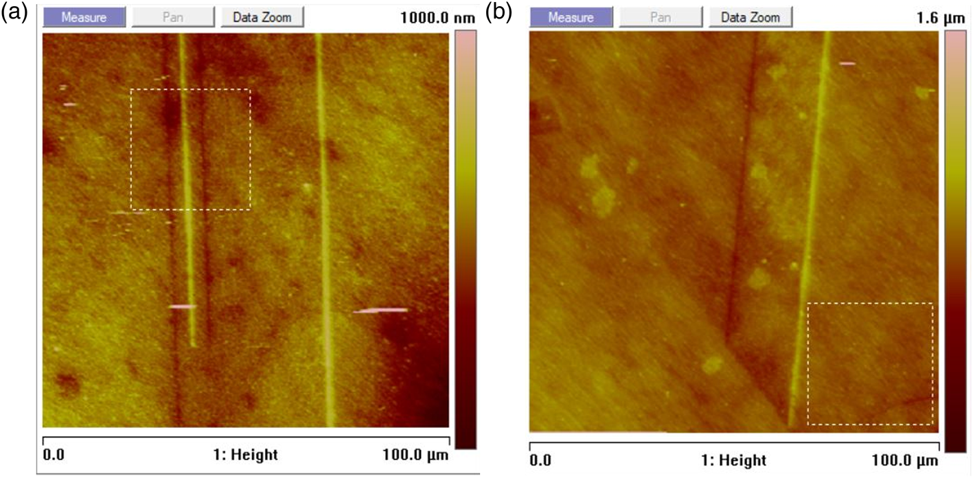
Fig. 5. 100 × 100 μm total area AFM scans showing twin formations. Darker lines represent grooves, while lighter lines represent peaks of twins intersecting the surface. Note that the surface roughness needs to be less than the depth and height of the boundaries for them to be clearly seen. The surface roughness of areas without planar defects is less than the one with twins, see Table 2. (a) A 30 × 30 μm box in the upper portion of the image shows the selected area for surface roughness evaluation with twins. (b) A 30 × 30 μm box in the lower right corner of the image shows the selected area for surface roughness evaluation with no twins.

Fig. 6. AFM line profile measurements showing the direct measurements of the vertical distance H for the groove (a) and H′ for the peak (b). The horizontal distance to the left, X L, and to the right, X R, from the min/max point of the grooves and peaks as shown. The angles, α and β, calculated from the vertical and horizontal distance measurements are shown for both grooves (a) and peaks (b).
Table 1. RMS Surface Roughness, S q, and Average Surface Roughness, S a, of 30 × 30 μm Area With and Without Twins.

See Figure 4 for selected areas on representative AFM images.
Table 2. Average Vertical Distance (Depth/Height) Measured with Respect to Leveled Background, Boundary Opening Width and AFM Measured Angles Associated with the Dihedral Angle for Both Grooves and Peaks.

The average dihedral angles, D and D′, are found to be 167 ± 5° and 193 ± 4°, respectively. The calculated ratio of interfacial energies, γ T/γ S, is found to be 0.0018, see equation (1). The sum of two orientation derivatives is 0.225, see equation (2).
EDS Mapping
EDS elemental mapping showed the homogeneous distribution of Cu and Zn, as expected according to the nominal composition of the alloy, with the detectable presence of oxides and carbon-based contaminations. The selected area compositional analysis was also performed to map more localized distributions of elements (Fig. 7). The compositions only vary a small amount depending on the area selected, see Table 3, which indicates statistical variation in composition from one area to another. The calculated total composition based on the spectrum shown in Figure 8, red numbers in column inset, amounts to 90.4 wt%Cu and 9.6 wt%Zn. Carbon and oxygen are excluded from the analysis. Exponential, XPP (exponential model of Pouchou and Pichoir matrix correction), correction (Pouchou et al., Reference Pouchou, Pichoir and Boivin1990) for calculating the quantitative amount of elements present were applied to refine EDS data. XPP is the AZtec equivalent to atomic number (Z), absorption (A), fluorescence (F) effect, or ZAF correction (Goldstein et al., Reference Goldstein, Newbury, Joy, Lyman, Echlin, Lifshin, Saywer and Michael2007). The calculated amount of 10 wt%Zn with XPP correction is in better agreement with the nominal value.

Fig. 7. Rectangular selected areas drawn at various locations over the entire SE image, total scan area ~2.5 × 2 mm. X-ray spectrum from each area was analyzed for elemental composition, see Table 3.

Fig. 8. X-ray spectrum from the elements present in the sample. A small sub-widow on the right shows the calculated weight % composition based on X-ray spectrums if the presence of both carbon and oxygen is considered (in yellow) and excluded (in red).
Table 3. Selected Area Compositional Analysis Verification on Cu10 wt%Zn Alloy.

The oxygen and carbon are excluded from analysis as they are surface contaminations.
Discussion
XY measurements obtained by different techniques are found to be in good agreement with each other. The opening width for boundaries is found to be ~1 μm based on AFM measurements, which is greater than SEM estimates of ~0.5 μm. The ambiguity in the outcome may be rooted in the nature of the contrast formation for secondary electrons in SEM (Goldstein et al., Reference Goldstein, Newbury, Joy, Lyman, Echlin, Lifshin, Saywer and Michael2007), tip to surface relation in AFM (Binnig et al., Reference Binnig, Quate and Gerber1986; Villarrubia, Reference Villarrubia1997), and cursor positioning in image analysis. Topographic contrast arises from trajectories and the number of secondary electrons which depend on the angle of incidence between the beam and incident surface. A tilted surface yields more secondary electrons than a surface normal to the beam. Therefore, if the topography is shallow (the surface is relatively smooth if the tilt angle is small), the contrast is expected to be weak. In the case of twin boundaries, the electron beam, at no tilt to the sample, visualizes the very bottom of the grooves and the ridges of the peaks. The sidewall visualization is expected to be poor due to the shallow topography.
AFM measurements are very sensitive to tiny topography variations, but results are subject to tip dilation effect (Villarrubia, Reference Villarrubia1997; Wong et al., Reference Wong, West, Olson, Mecartney and Starostina2007). Tip dilation artifacts tend to make grooves appear narrower and peaks appear wider by the size of the probe. The height measurements are expected to be accurate and unaffected by tip artifacts. The depth measurements can be affected by the aspect ratio and/or the half cone angle at the apex of the tip. This effect is most pronounced for narrow trenches with vertical walls (Villarrubia, Reference Villarrubia1997; West & Starostina, Reference West and Starostina2003). Considering the geometry of the probes used, the tip artifact may have a slight contribution to a consistent difference between height and depth measurements, 158 versus 118 nm. The bigger contribution may come from an ambiguity of cursor positioning on a line profile. This results in a large standard deviation in Z (~45 nm) and XY distance measurements (~700 nm). All these factors in their turn affect dihedral angle measurements. Interestingly, Mykura points out in his paper (Mykura, Reference Mykura1957) that the accuracy of the ratio twin/surface free energy is poor, but the value of the sum of two orientation derivatives should be quite reliable, see equation (2).
Mykura's values for the dihedral angles of twin-boundary grooves in nickel using optical interferometry are 175° for D and 183° for D′ on average. The calculated ratio for γ T/γ S is 0.005. The sum of two orientation derivatives is 0.05. The values for copper and gold obtained by other researchers (Brooks, Reference Brooks1951; Fullman, Reference Fullman1951; Buttner et al., Reference Buttner, Udin and Wulff1953; Mykura, Reference Mykura1957) are summarized in Table 4. AFM experiment measured averages for D and D′ angles are 167 ± 5° and 193 ± 4°, respectively. The calculated ratio of interfacial energies is γ T/γ S = 0.0018, and the sum of two orientation derivatives is 0.225. Our results are in good agreement with previously reported data, which affirms the feasibility of using AFM as a tool for dihedral angle measurements.
Table 4. Comparative Table of the Energy Ratio and the Sum of Two Orientation Derivatives Reported by Various Research Groups.

All previous efforts from the aforementioned research are done using pure FCC metals. This work is focused on a CuZn alloy. According to the literature (Kaygisiz, Reference Kaygisiz2009; Zhevnenko, Reference Zhevnenko2016), the amount of alloying affects interfacial free energies of the surface, which may or may not account for the shift in the dihedral angle of the twin boundaries. An extensive literature survey has not found dihedral angle measurements done on binary alloys. Additional factors contributing to interfacial free energies and their ratio may be surface oxidation (Mykura, Reference Mykura1967), crystallographic orientation (Mykura, Reference Mykura1957, Reference Mykura1967), or surface roughness. It has been reported by Mykura (Mykura, Reference Mykura1967) that silver free of oxygen does not show the energy dependence effect on crystallographic orientation. The silver–oxygen system does show the dependency. It is reported that the (111) and (100) planes have surface free energies of about 15% less than the value at random surfaces. Our EDS measurements indicate the presence of oxidation and carbon-based contaminations of the surface. The composition across the sample is found to be homogeneous. The surface roughness of the sample may also contribute to the experimental error of angle determination as it allows for an ambiguity of the vertical and lateral distance measurements. Surface roughness measurements were done on selected 30 μm × 30 μm areas with and without twin boundaries present. The S a and S q, of selected areas without planar defects, 48.3 and 38.6 nm, are found to be less than those with twins, 61.9 and 44.7 nm. The average measured height/depth of the boundaries lie in the range of 118–158 nm or two to four times greater than surface roughness. Further investigation may be necessary to address the specifics of all contributing factors.
Conclusions
AFM has been proven for the first time to be a feasible new method for measuring the dihedral angles of twin-boundary grooves. Twin-boundary characteristic dimensions (width, opening width, depth, height, and dihedral angle) have been evaluated by AFM. 2D morphology results obtained by different techniques are consistent with each other. EDS analysis confirmed the composition of the material to be within reasonable agreement to nominal composition, Cu10 wt%Zn, considering the detectable presence of carbon-based contaminations and oxidation. The average and RMS surface roughness are greater if planar defects are present based on selected area measurements. The average range of depth and height of the grooves and peaks is 118 ± 45 and 158 ± 45 nm, respectively, and two to four times greater than surface roughness. The dihedral angle measurements of twin-boundary grooves and peaks using AFM methods were found to be 167 ± 5° and 193 ± 4°, respectively. The twin to surface interfacial free energy ratio is calculated to be 0.0018. The sum of two orientation derivatives is 0.225. Our results are consistent with previously reported data.
Acknowledgments
We acknowledge the contributions of Dr. R. Mark's scientific insights and sample availability, and Prof. Drazen Fabris for supporting and funding the MECH 333B course. A special thanks for the commitment and dedication of our Teacher Assistants for this course—graduate student Dongmeng Li and PhD student Vinay Krishnan for SEM/EDS and AFM data acquisition, respectively.


 Open access