Hostname: page-component-848d4c4894-5nwft Total loading time: 0 Render date: 2024-05-06T23:01:29.760Z Has data issue: false hasContentIssue false

Focused Ion Beam Preparation of Low Melting Point Metals: Lessons Learned From Indium

Published online by Cambridge University Press:  22 March 2022

Joseph R. Michael*
Affiliation:
Material, Physical, and Chemical Sciences Center, Sandia National Laboratory, PO Box 5800, Albuquerque, NM 87185-0886, USA
Daniel L. Perry
Affiliation:
Material, Physical, and Chemical Sciences Center, Sandia National Laboratory, PO Box 5800, Albuquerque, NM 87185-0886, USA
Damion P. Cummings
Affiliation:
Material, Physical, and Chemical Sciences Center, Sandia National Laboratory, PO Box 5800, Albuquerque, NM 87185-0886, USA
Jeremy A. Walraven
Affiliation:
MESA: Microsystem Engineering, Science, and Applications, Sandia National Laboratory, PO Box 5800, Albuquerque, NM 87185-1072, USA
Matthew B. Jordan
Affiliation:
MESA: Microsystem Engineering, Science, and Applications, Sandia National Laboratory, PO Box 5800, Albuquerque, NM 87185-1084, USA
*
*Corresponding author: Joseph R. Michael, E-mail: jrmicha@sandia.gov
Get access

Abstract

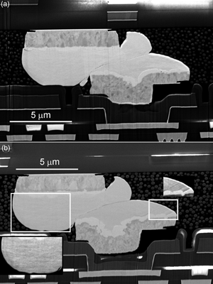
Indium (In) and other low melting point metals are used as interconnects in a variety of hybridized circuits and a full understanding of the metallurgy of these interconnects is important to the reliability and performance of the devices. This paper shows that room temperature focused ion beam (FIB) preparation of cross-sections, using Ga+ or Xe+ can result in artifacts that obscure the true In microbump structure. The use of modified milling strategies to minimize the increased local sample temperature are shown to produce cross-sections that are representative of the In bump microstructure in some sample configurations. Furthermore, cooling of the sample to cryogenic temperatures is shown to reliably eliminate artifacts in FIB prepared cross-sections of In bumps allowing the true bump microstructure to be observed.

Type
Materials Science Applications
Copyright
Copyright © The Author(s), 2022. Published by Cambridge University Press on behalf of the Microscopy Society of America

Access options

Get access to the full version of this content by using one of the access options below. (Log in options will check for institutional or personal access. Content may require purchase if you do not have access.)

References

Anderson, T & Ansara, I (1991). The Ga-In (gallium-indium) system. J Phase Equilib 12(1), 6472.10.1007/BF02663677CrossRefGoogle Scholar
Bassim, N, De Gregorio, B, Kilcoyne, A, Scott, K, Chou, T, Wirick, S, Cody, G & Stroud, R (2012). Minimizing damage during FIB sample preparation of soft materials. J Microsc 245(3), 288301.10.1111/j.1365-2818.2011.03570.xCrossRefGoogle Scholar
Behrisch, R & Eckstein, W (1993). Sputtering yield increase with target temperature for Ag. Nucl Instrum Methods Phys Res B 82(2), 255258.10.1016/0168-583X(93)96027-ACrossRefGoogle Scholar
Bohdansky, J & Roth, J (1987). Temperature dependence of sputtering behavior of Cu-Li alloys. Nucl Instrum Methods Phys Res B 23(4), 518520.10.1016/0168-583X(87)90479-4CrossRefGoogle Scholar
Boulesteix, C, Devant, G, Marraud, A & Rateau, R (1969). Structure and recrystallization of indium thin film. J Vac Sci Technol 6(4), 780783.10.1116/1.1315759CrossRefGoogle Scholar
Broennimann, C, Glaus, F, Gobrecht, J, Heising, S, Horisberger, M, Horisberger, R, Kästli, H, Lehmann, J, Rohe, T & Streuli, S (2006). Development of an indium bump bond process for silicon pixel detectors at PSI. Nucl Instrum Methods Phys Res A 565(1), 303308.10.1016/j.nima.2006.05.011CrossRefGoogle Scholar
Brostow, W, Gorman, BP & Olea-Mejia, O (2007). Focused ion beam milling and scanning electron microscopy characterization of polymer+ metal hybrids. Mater Lett 61(6), 13331336.10.1016/j.matlet.2006.07.026CrossRefGoogle Scholar
Cen, X & van Benthem, K (2018). Ion beam heating of kinetically constrained nanomaterials. Ultramicroscopy 186, 3034.10.1016/j.ultramic.2017.12.005CrossRefGoogle ScholarPubMed
Cheng, X, Liu, C & Silberschmidt, V (2009). Intermetallics formation and evolution in pure indium joint for cryogenic application. In 11th Electronics Packaging Technology Conference, pp. 562–566. IEEE.10.1109/EPTC.2009.5416484CrossRefGoogle Scholar
Chou, T & Williams, ME (2014). Cryo-FIB minimizes Ga+ milling artifacts in Sn. Microsc Microanal 20(S3), 328329.10.1017/S1431927614003365CrossRefGoogle Scholar
Dang, T, Shima, D, Balakrishnan, G, Chen, A & Bedford, RG (2012). Low homologous temperature (<0.2) sputtering of indium films on silicon. J Vac Sci Technol B Nanotechnol Microelectron 30(6), 060602.10.1116/1.4753818CrossRefGoogle Scholar
Das, RN, Yoder, J, Rosenberg, D, Kim, D, Yost, D, Mallek, J, Hover, D, Bolkhovsky, V, Kerman, A & Oliver, W (2018). Cryogenic qubit integration for quantum computing. In IEEE 68th Electronic Components and Technology Conference (ECTC), pp. 504–514. IEEE.10.1109/ECTC.2018.00080CrossRefGoogle Scholar
Dasarathy, C (1970). Short communications and laboratory/tips labortips und rezepte. Pract Metallogr 7(1), 4446.10.1515/pm-1970-070108CrossRefGoogle Scholar
de Morais, LD, Chevalliez, S & Mouleres, S (2014). Low temperature FIB cross section: Application to indium micro bumps. Microelectron Reliab 54(9–10), 18021805.10.1016/j.microrel.2014.08.004CrossRefGoogle Scholar
Deppisch, C, Fitzgerald, T, Raman, A, Hua, F, Zhang, C, Liu, P & Miller, M (2006). The material optimization and reliability characterization of an indium-solder thermal interface material for CPU packaging. JOM 58(6), 6774.10.1007/s11837-006-0186-6CrossRefGoogle Scholar
Famá, M, Shi, J & Baragiola, R (2008). Sputtering of ice by low-energy ions. Surf Sci 602(1), 156161.10.1016/j.susc.2007.10.002CrossRefGoogle Scholar
Foxen, B, Mutus, J, Lucero, E, Graff, R, Megrant, A, Chen, Y, Quintana, C, Burkett, B, Kelly, J & Jeffrey, E (2017). Qubit compatible superconducting interconnects. Quantum Sci Technol 3(1), 014005.10.1088/2058-9565/aa94fcCrossRefGoogle Scholar
Fu, J, Joshi, SB & Catchmark, JM (2008). Sputtering rate of micromilling on water ice with focused ion beam in a cryogenic environment. J Vac Sci Technol A 26(3), 422429.10.1116/1.2902962CrossRefGoogle Scholar
Giannuzzi, LA & Stevie, FA (2004). Introduction to Focused ion Beams: Instrumentation, Theory, Techniques and Practice. New York, New York: Springer.Google Scholar
Gorman, B, Sahu, L, Shaito, A, Nandika, D, Olea-Mejia, O & Brostow, W (2006). FIB/FESEM investigations of polymer/inorganic composites. Microsc Microanal 12(S02), 10001001.10.1017/S143192760606716XCrossRefGoogle Scholar
Hayles, M, Stokes, D, Phifer, D & Findlay, K (2007). A technique for improved focused ion beam milling of cryo-prepared life science specimens. J Microsc 226(3), 263269.10.1111/j.1365-2818.2007.01775.xCrossRefGoogle ScholarPubMed
Huang, Q, Xu, G, Yuan, Y, Cheng, X & Luo, L (2010). Development of indium bumping technology through AZ9260 resist electroplating. J Micromech Microeng 20(5), 055035.10.1088/0960-1317/20/5/055035CrossRefGoogle Scholar
Ishitani, T & Kaga, H (1995). Calculation of local temperature rise in focused-ion-beam sample preparation. Microscopy 44(5), 331336.Google Scholar
Lei, CU, Krayzman, L, Ganjam, S, Frunzio, L & Schoelkopf, RJ (2020). High coherence superconducting microwave cavities with indium bump bonding. Appl Phys Lett 116(15), 154002.10.1063/5.0003907CrossRefGoogle Scholar
Li, J & Liu, P (2017). Important factors to consider in FIB milling of crystalline materials. In Characterization of Minerals, Metals, and Materials 2017, Ikhmayies, S, Li, B, Carpenter, JS, Li, J, Hwang, J-Y, Neves Monteiro, S, Firlplarao, D, Zhang, M, Peng, Z, Escobedo-Diaz, JP, Bai, C, Eren Kalay, Y, Goswami, R & Kim, J (Eds.), pp. 329336. Cham, Switzerland: Springer.10.1007/978-3-319-51382-9_36CrossRefGoogle Scholar
Lin, Y, Hung, H, Yu, H, Kao, C & Wang, Y (2020). Phase stabilities and interfacial reactions of the Cu–In binary systems. J Mater Sci: Mater Electron 31, 13.Google Scholar
Matsushima, H, Suzuki, T & Nokuo, T (2013). An evaluation of FIB cross-sectioning using a cooling stage for metals and alloys with low melting point. Mater Sci Forum 753, 36.10.4028/www.scientific.net/MSF.753.3CrossRefGoogle Scholar
Mayer, J, Giannuzzi, LA, Kamino, T & Michael, J (2007). TEM sample preparation and FIB-induced damage. MRS Bull 32(5), 400407.10.1557/mrs2007.63CrossRefGoogle Scholar
Nelson, RS (1965). An investigation of thermal spikes by studying the high energy sputtering of metals at elevated temperatures. Philos Mag 11(110), 291302.10.1080/14786436508221857CrossRefGoogle Scholar
Reed, R, McCowan, CN, Walsh, R, Delgado, L & McColskey, J (1988). Tensile strength and ductility of indium. Mater Sci Eng A 102(2), 227236.10.1016/0025-5416(88)90578-2CrossRefGoogle Scholar
Rogalski, A (2012). Progress in focal plane array technologies. Prog Quantum Electron 36(2–3), 342473.10.1016/j.pquantelec.2012.07.001CrossRefGoogle Scholar
Rosenberg, D, Kim, D, Das, R, Yost, D, Gustavsson, S, Hover, D, Krantz, P, Melville, A, Racz, L & Samach, G (2017). 3D integrated superconducting qubits. NPJ Quantum Inf 3(1), 15.10.1038/s41534-017-0044-0CrossRefGoogle Scholar
Shukla, N, Tripathi, SK, Banerjee, A, Ramana, ASV, Rajput, NS & Kulkarni, VN (2009). Study of temperature rise during focused Ga ion beam irradiation using nanothermo-probe. Appl Surf Sci 256(2), 475479.10.1016/j.apsusc.2009.07.024CrossRefGoogle Scholar
Soussan, P, Majeed, B, Le Boterf, P & Bouillon, P (2015). Evaluation of Sn-based microbumping technology for hybrid IR detectors, 10μm pitch to 5μm pitch. In IEEE 65th Electronic Components and Technology Conference (ECTC), pp. 597–602. IEEE.10.1109/ECTC.2015.7159652CrossRefGoogle Scholar
Thomas, C, Charbonnier, J, Garnier, A, Bresson, N, Bouchu, D, Moreau, S, Gustavo, F & Vinet, M (2021). Electrical and morphological characterizations of 3D interconnections for quantum computation. IEEE Trans Compon Packag Manuf Technol. doi:10.1109/TCPMT.2021.3104326.Google Scholar
Tian, Y, Hutt, DA, Liu, C & Stevens, B (2009 a). High density indium bumping through pulse plating used for pixel X-ray detectors. In International Conference on Electronic Packaging Technology & High Density Packaging, pp. 456–460. IEEE.Google Scholar
Tian, Y, Liu, C, Hutt, D & Stevens, B (2014). Electrodeposition of indium bumps for ultrafine pitch interconnection. J Electron Mater 43(2), 594603.10.1007/s11664-013-2891-6CrossRefGoogle Scholar
Tian, Y, Liu, C, Hutt, D, Stevens, B, Flynn, D & Desmulliez, MP (2009 b) High density indium bumping using electrodeposition enhanced by megasonic agitation. In 11th Electronics Packaging Technology Conference, pp. 31–35. IEEE.Google Scholar
Tu, K-N (2011). Reliability challenges in 3D IC packaging technology. Microelectron Reliab 51(3), 517523.10.1016/j.microrel.2010.09.031CrossRefGoogle Scholar
Tu, K-N & Zeng, K (2002). Reliability issues of Pb-free solder joints in electronic packaging technology. In 52nd Electronic Components and Technology Conference (Cat. No. 02CH37345). pp. 1194–1200. IEEE.CrossRefGoogle Scholar
Vander Voort, GF, Lampman, SR, Sanders, BR, Anton, GJ, Polakowski, C, Kinson, J, Muldoon, K, Henry, SD & Scott, WW Jr. (2004). ASM handbook. Metallogr Microstruct 9, 278279.Google Scholar
Volkert, CA & Minor, AM (2007). Focused ion beam microscopy and micromachining. MRS Bull 32(5), 389399.10.1557/mrs2007.62CrossRefGoogle Scholar
Wang, Y-W & Kao, CR (2019). Interfacial reactions of Cu and In for Low-temperature processes. In IEEE 21st Electronics Packaging Technology Conference (EPTC), pp. 435–439. IEEE.10.1109/EPTC47984.2019.9026712CrossRefGoogle Scholar
Windawi, H (1976). Effect of temperature on the sputtering yield of copper. Surf Sci 55(2), 573588.10.1016/0039-6028(76)90258-2CrossRefGoogle Scholar
Yao, N (2007). Focused ion Beam Systems: Basics and Applications. New York: Cambridge University Press.10.1017/CBO9780511600302CrossRefGoogle Scholar